Design and Implementation Of Low Power CMOS Full Adder Circuit in Nano scale
CMOS Processes
Saima Ayyub and Awadhesh.K.G.Kandu Dept of Electronics & Telecommunication Lakshmi Narain College of Technology,Bhopal
Abstract
Today’s leakage reduction is an important task to improve the performance of CMOS circuit with the power loss scenario. Leakage is mainly due to the scaling of CMOS. There are static and dynamic (switch mode) power losses occurs in CMOS circuit, in which static power is more important for sleep mode (no operation mode), leakage reduction improves the efficiency of the circuit, thereby saving a significant amount of energy. In static mode power consumption is the major drawback. As the biasing is remain in the internal circuit of the system there will be more sources of leakage in the internal circuits. In nano scale there are many sources (low threshold voltage, very thin gate oxide layer and band to band tunneling) which are responsible for the leakage of current. This paper propose an approach of using a power gating switch (PGS) to minimize the leakage of power because of fine scaling of CMOS. The purpose of employing PGSs in circuits is to reduce sleep power by strongly shut off the leakage paths during sleep modes, means there is no close loop between supply and ground. In this method at stand by condition leakage current will be minimized. Circuits are simulated in MICROWIND using 90nm and 45nm CMOS technology. The simulations will show leakage consumption can greatly be reduced by using the proposed power-gating switch compared with the MTCMOS power-gating Technique.
Keywords
MTCMOS, power gating switch, sleeps mode, standby mode, sub-threshold leakage, Clock Adiabatic Logic(CAL)
I.
Introduction
In most recent CMOS feature sizes (e.g., 90nm and 45nm), leakage power dissipation has become an overriding concern for VLSI circuit designers. International technology roadmap for semiconductors (ITRS) reports that leakage power dissipation may come to dominate total power consumption. Power consumption of CMOS consists of dynamic and static components. Dynamic power is consumed when transistors are switching or active and static power is consumed regardless of transistor switching.
Many previously proposed techniques, such as voltage and frequency scaling, on dynamic power reduction. However, as the feature size shrinks, e.g., to 45 nm and 90nm, static power has become a great challenge for current and future technologies. This dissertation implements 4bit CMOS parallel adder circuit with an addition of clocked adiabatic
logic with a power gating switch consisting of sleep transistor to minimize the leakage
Components of Power Dissipation are
Pavg=P switching +P short-circuit +P leakage C L .V DD 2 F clk +I SC .V DD +I Leakage .V DD
There are many reasons for which leakage power losses occur in CMOS circuit.[3]
Sub-threshold leakage (weak inversion current)
Gate oxide leakage (Tunneling current)
Channel punch through
Drain induced barrier lowering
Figure 1 : Leakage power components in CMOS
.
There are several sources for the leakage currents: (i) sub threshold leakage current due to very low threshold voltage (VT), (ii) gate leakage current due to very thin gate oxide (TOX), (iii) Band-to-Band tunneling leakage current due to heavily doped halo. As a result of an exponential dependency on the reduction of the threshold voltage, sub-threshold leakage has the potential to become the dominant factor in sub-100nm generations [2, 3].
variable threshold CMOS (VTCMOS), However, these techniques
Adiabatic logic is a promising low-power method to reduce the energy dissipation in digital circuits. Several adiabatic logic families and their applications have been reported and achieved considerable energy savings [5-7]. Similar to power-gating techniques of conventional CMOS circuits, power-gating schemes for adiabatic circuits have been also introduced to reduce energy loss during idle periods [8, 9]. However, the previously reported power-gating adiabatic circuits are mostly investigated for reducing their dynamic energy dissipations during idle periods require significant circuit modification and performance overhead for leakage reduction[6][7].
This dissertation implements 4bit and 8 bit CMOS parallel full addercircuit with an addition of clocked adiabatic logic with a power gating switch consisting of sleep transistor to minimize the leakage
II.
CAL CIRCUIT
In this thesis work, a new CMOS logic family called ADIABATIC LOGIC, based on the adiabatic switching principle is presented. The term adiabatic comes from thermodynamics, used to describe a process in which there is no exchange of heat with the environment. The adiabatic logic structure dramatically reduces the power dissipation. The adiabatic switching technique can achieve very low power dissipation, but at the expense of circuit complexity. Adiabatic logic offers a way to reuse the energy stored in the load capacitors rather than the traditional way of discharging the load capacitors to the ground and wasting this energy.
The supply voltage in adiabatic circuits in addition to providing the power to the circuit behaves as the clock of the circuit and for this reason is called power clock. One of the main concerns in the adiabatic logic circuits is the power clock generation. In these circuits the supply voltage is desired to be a ramping voltage.
Although. it can be approximated by a sinusoidal voltage The improved CAL buffer is shown in Fig. 2(a) [7][9]. The logic evaluation circuit consists of the two NMOS transistors (N1, N2). CX is an auxiliary clock signal, and it enables the evaluation NMOS transistors (N1, N2) by turning on the NMOS transistors (N5, N6). The energy recovery circuit consists of the two cross-coupled PMOS transistors (P1, P2).power-clock (clk) charges the output (OUT or OUTb) in evaluation phase through P1 and P2. In recovery phase, the energy of the output nodes is recovered to clk through P1 and P2. The clamp transistors (N3 and N4) ensure stable operation by preventing from floating of the output nodes. The improved CAL circuits are supplied by a single-phase power clock, as shown in Fig. 2(a). The two phase non-overlap sinusoidal clocks (CX and CXb) are used for the auxiliary lines, as shown in Fig. 2(b). The two-phase sinusoidal clocks are generated with an auxiliary clock generator, as shown in Fig. 2(c) [7]. Its simulated waveforms are also shown in Fig. 2(d)
Figure 2(a) CAL Buffer Circuit[7]
Figure 2(b) Simulation Waveform
Figure 2(c) Clock Generator[7]
III.
Transmission Gate for Sleep Approach
In the sleep approach, both (i) An additional "sleep" PMOS transistor is placed between VDD and the pull-up network of a circuit and (ii) An additional "sleep" NMOS transistor is placed between the pull-down network and GND. These sleep transistors turn off the circuit by cutting off the power rails. Figure 1 shows its structure. The sleep transistors are turned on when the circuit is active and turned off when the circuit is idle. By cutting off the power source, this technique can reduce leakage power effectively.
Similar to power-gating techniques of conventional CMOS circuits, adiabatic units can be also shut down by switching off their power-clocks to reduce energy loss during idle periods. The power-gating scheme for the improved CAL circuits is shown in Fig. 3. The transmission gate (TG) is used as the power-gating switch, which is inserted between the single phase power-clock (pc) and virtual power-clock (clk). It is used to disconnect the power-gated CAL logic blocks during idle periods In active mode, the power-gating control signal (Active) is high, thus clk follows the power-clock (pc). In sleep mode, Active is low, thus clk is set as low level, so that the power gated the power-gating adiabatic logic block.
Figure 3(a) Sleep Approach
Figure 3(b) Transmission gate using sleep input in3
Figure 3(c) Transmission Gate timing Waveform
IV.
Motivation
Digital CMOS integrated circuits have been the driving force behind VLSI for high performance computing and other applications related to science and technology. The demand for digital CMOS integrated circuits will continue to increase in the near future ,due to its important silent features like low power ,reliable performance and improvements in the processing technology. large power dissipation requires larger heat sinks hence increased area. Cost of providing power has resulted in significant interest in power reduction of non portable devices sleep energy ,which has become important in modern CMOS processes due to increasing contributions of sub threshold and gate .Leakage current which affects total power consumption ,and affects battery life. Therefore we have motivated to perform dissertation work in the accurate relative power measurement for effective reduction of leakage in sleep mode with less complexity and no overhead in the circuit.
V.
Proposed Methodology
In this paper, we use an energy efficient power gating technique for adiabatic circuits.. Transmission gates with sleep transistors are used as the power-gating switches.
A 4 bit full adder based circuits is verified using the proposed power-gating technique. Energy consumption of the CAL based circuit is simulated as a function of frequency. The proposed approach demonstrates that the circuit reduces considerable amount of leakage power in the Nano scale CMOS integrated circuits and are simulated in 45nm, 90nm and technology using MICRO-WIND EDA tool.
Desired power-clock frequency f, which is fed to the adiabatic block having frequency f =√1/2 LCeq In the clock period A,
the auxiliary clock CX enables the logic evaluation. For out= 0, compliment of function block are on, causing outb= 0 and M1 to be on, and thus allowing output out2 to closely follow the power clock waveform. In the next clock period B, the auxiliary clock CX = 0 disables the logic evaluation. The previously stored logic state repeats at the outputs out1 and out2 regardless of the inputs, so that the stage that follows can perform logic evaluation. The logic evaluation is enabled in alternate logic stages by the auxiliary clock CX and its complement CX, at half the power clock rate.[7][9]
used to disconnect the adiabatic logic block from the power-clocks during idle periods.
Fig. 4 Flow Chart
In order to reduce additional energy loss and obtain full swing operation of power gating switches should be energy efficient .The control signals „sleep‟ feed the gates of S1 and S2 respectively. The sleep transistors S1 and S2 are high threshold voltage devices and the logic gate transistors are standard threshold voltage devices. This is to provide a well balanced trade-off between high speed and leakage loss. The CMOS circuit output can be drawn either between PUN and sleep circuit or between sleep circuit and PDN.[14]
In standby mode when sleep input is 1 power clock is disconnected from the functional block .devices s1 and s2 are high threshold devices therefore sub threshold conduction reduces at the cost of scaling of devices in 45nm and 90 nm .there.fore reduces leakge current and thus total power consumtion reduces.
VI.
Implementation
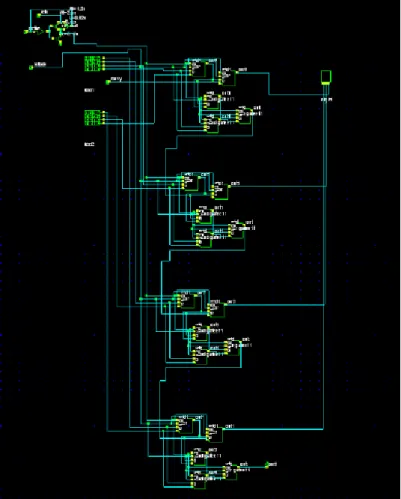
A 4 bit CMOS adder circuit is implemented in DSCH tool. Functional block is made up with adiabatic logic. A sinusoidal clock is supplied to the adiabatic logic. Power gating switch is used for providing supply voltage in active mode. And shut off the supply in standby mode.
Figure 5 Implementation of 4-Bit fulladder in MICROWIND
VII.
RESULTS
Compared with MTCMOS proposed scheme can well reduce the total power consumption .At 90 nm CMOS technology, the 4 bit improved CAL adder with MTCMOS scheme attains energy savings of 13.2.9% to 19.6% with the frequency changing from 1000 to 3000 MHz .
At 45 nm CMOS technology, the 4 bit improved CAL adder with MTCMOS scheme attains energy savings of 26.2% to 27.0% with the frequency changing from 1000 to 3000 MHz.
Tab 1& Tab 2shows the leakage power consumption reduction and the total power consumption reduction of 4 bit improved CAL adders with proposed scheme compared with the MTCMOS in 45nm CMOS technology and 90 nm CMOS technology ,respectively. As we can see that Tab1 and Tab2 with the scaling of reduction of processes ,the leakage power loss of CAL circuits can be reduced more effectively by using power gating switch.
TABLE:1 POWER LOSS REDUCTION OF 4 BIT CAL FULL ADDER USING POWER GAITNG SWITCH AT 45nm PROCESS COMPARED WITH BASE CASE
%Power Reduction
(45nm)
Frequency(MHz)
1000 2000 3000
STATIC POWER 45.6 41.3 37
TOTAL POWER
CONSUMPTION 27.6 27 26.8
TABLE:2 POWER LOSS REDUCTION OF 4 BIT CAL FULL ADDER USING POWER GAITNG SWITCH AT 45nm PROCESS COMPARED WITH BASE CASE
%Power Reduction
(120nm)
Frequency(MHz)
1000 2000 3000
STATIC POWER 37.8 35.6 35.4
TOTAL POWER
CONSUMPTION 19.1 17.3 13.2
VIII.SIMULATION
Fig:7(b) SIMULATION WAVEFORM OF 4 BIT CAL FULL ADDER IN MICROWIND
Fig:7(c) LEAKAGE CURRENT IN 4 BIT CAL FULL ADDER(GREEN)
Fig:7(d) TIMING WAVEFORM OF 4 BIT CAL FULL ADDER
IX.CONCLUSION
This paper presents designing and simulation of low power CMOS full adder circuit. results shows that by introducing a power gating switch ,leakage power loss and total power loss of 4 bit and 8 bit adder can be reduced by 20-30 percent .
REFERENCES
[1] An Adiabatic Single-Phase MTCMOS Scheme for Leakage Reduction in Nano -Scale CMOS Processes Li Su and Jianping Hu Faculty of Information Science and Technology Ningbo University Ningbo City, Zhejiang 315211, China.
[2] N. S. Kim, T. Austin, et al., “Leakage current: Moore‟s law meets static power”, Computer, pp. 68-75, Vol. 38(12), 2003.
[3] Kaushik Roy, et.al., “Leakage Current Mechanisms and Leakage Reduction Techniquesin Deep-Submicrometer CMOS Circuits”, IEEE, VOL.91,NO.2, pp.305-327, 2003.
[4] F. Fallah, M. Pedram, “Standby and active leakage current control and Minimization in CMOS VLSI circuits”, IEICE Transactions on Electronics, pp. 509–519, Vol. E88–C (4), 2005.
[6] F. Liu and K. T. Lau, “Pass-transistor adiabatic logic with NMOS pulldown configuration,” Electronics Letters, vol. 34, no. 8, 1998, pp. 739−741.
[7] D. Maksimovic, V. G. Oklobdzija, B. Nikolic, and K. W. Current, “Clocked CMOS adiabatic logic with integrated single-phase powerclock supply,” IEEE Trans. VLSI Syst., vol. 8, 2000, pp. 460–463.
[8] Changning Luo and Jianping Hu, “Single-phase adiabatic flip-flops and sequential circuits using improved CAL circuits,” IEEE International Conference on ASIC (AICON 2007), Guilin, China, 2007, pp. 126-129.
[9] Dong Zhou, Jianping Hu, and Huiying Dong, “An energy-efficient power-gating adiabatic circuits using transmission gate switches” , IEEE ASICON‟07, pp. 145-148, 2007.
[10] Weiqiang Zhang, Li Su, Jinghong Fu, and Jianping Hu, “A power-gating scheme for CAL circuits using single-phase power-clock”, 2008 IEEE Asia Pacific Conference on Circuit and Systems, pp. 846-849, 2008.
[11] Wei Zhao and Yu Cao, “New generation of Predictive Technology Model for sub-45nm design exploration”, Department of Electrical Engineering, Arizona State University, 2006.
[12] Hiroshi Kawaguchi,Koichi Nose and Takayasu sakurai,” A S upper cut off CMOS (SCCMOS) S cheme for 0.5 V S upply Voltage with picoampere Stand By Current.
[13] IEEE Transactions On Very Large Scale Integration (VLSI) Systems, Vol. 20, No. 4, April 2012 605 Sleep Mode Analysis and Optimization With Minimal-Sized Power Gating Switch for Ultra-Low vdd Operation Mingoo Seoket.al