A Grid Level High Power Back To Back System Using Modular
Multilevel Cascade Converter Without Dc Link Capacitor
Nikhilesh Reddy1, Mr.Y.Raja Babu2 1
PG Scholar, Pydah College of Engineering, Kakinada, AP, India. 2Assistant Professor, Pydah College of Engineering, Kakinada, AP, India.
Abstract: In this paper a fuzzy logic controller have been designed for back-to back (BTB) system unifying two modular multilevel cascade converters (MMCCs). Based on double-star chopper cells BTB system designed. The two DSCCs connected back-to-back consist of multiple cascaded chopper cells and a center-tapped inductor. Low voltage steps bring significant reductions in harmonic voltage and current to the BTB system. Neither dc-link capacitor nor voltage sensors required for regulating the dc-link voltage and controlling theca-link current. A three-phase downscaled BTB system with three-phase-shifted PWM is designed, with fuzzy logic controller to verify its operating principles and performance. The fuzzy logic controller improves the performance of the BTB system, compared with the conventional system. Analytical, simulated results agree well with each other in steady and transient states. Simulation waveforms can be done with MATLAB/SIMULINK software, and shows the effectiveness of a self-starting procedure.
Keywords—Asynchronous intertie, back-to-back (BTB) systems, grid-connected power converters, modular multilevel cascade converters (MMCCs)
I INTRODUCTION
The HVDC system has, or will have, a dc-voltage range of 250 to 500 kV or higher to reduce the conducting power loss of overhead transmission lines and underground or undersea cables. On the other hand, the BTB system is more flexible in dc-link voltage design than the HVDC system because theft system can be considered as a “zero-meter-long” HVDC system. Therefore, it would be reasonable and acceptable forth BTB system to have a dc-link voltage as low as 66 kV or132 kV. THE modular multilevel cascade converter (MMCC) family consists of several members with different given names. These members have the common family name “MMCC” because they are characterized by cascade connections of either single-phase full-bridge (H-bridge) ac/dc converters called simply as “bridge-cells” or no isolated bidirectional dc/dc choppers called just as “chopper cells.” These family members have different characters from a practical point of view.
Among them, attention has been paid to the specific family member with the given name, “double-star chopper cells (DSCCs)” for grid connections and motor drives. Although the full name is “MMCC-DSCC,” this paper calls it simply as a “DSCC” for the sake of simplicity. The DSCC is the same in circuit configuration as a specific modular multilevel converter (MMC) presented in [2]–[4]. A difference exists in dc-link voltage between a
long-system. Another difference exists in control strategy between the HVDC and BTB systems. It lies in whether “real-time communications” between the two DSCCs are available or not. Theft system can detect actual voltages and currents in the two DSCCs and can send the detected signals to a unified digital controller because the two DSCCs are installed at the same site. In other words, the two DSCCs can be considered as a single power conversion system with the unified digital controller.
On the other hand, the HVDC system has a digital controller for each DSCC, in which the two digital controllers are operated independent of each other because one DSCC is too far away from the other to bring the unified digital controller to the HVDC system. In other words, the two DSCCs can be considered as two separate power conversion systems. As a result, the two DSCCs forming the BTB system can take the equal responsibility for regulating the dc-link voltage and controlling the dc-link current, whereas the two DSCCs forming the HVDC system should take different responsibilities. Research scientists and engineers in power electronics and power systems have presented or published technical papers on DSCC-based power conversion systems with focus on control, modeling, analysis, design, and/or operation. Some papers have included experimental waveforms obtained from single DSCC. However, neither paper nor article has disclosed actual waveforms obtained from a downscaled or commercially operating system consisting of two DSCCs connected back-to-back directly or with long cables. In addition, no careful comparison has been made among experiment, simulation, and analysis for the purpose of guaranteeing and enhancing their reliability.
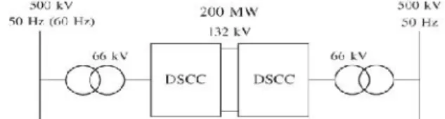
Fig. 1 Circuit configuration of the 200-MW DSCC-based BTB (FC) system
simulation is reliable enough to look into more practical systems and fault-ride-through (FRT) performance. Modeling and analysis are done for the single power conversion system unifying the two DSCCs that take the equal responsibility for regulating the dc-link voltage and controlling the dc-link current. A transient dc-link current to a small step change in the reference of active-power transfer from 8 to10 kW exhibits a first-order response with a time constant of about 0.9 ms in both experiment and simulation. This time constant agrees well with a theoretical time constant of 0.94 ms. Moreover, this paper presents experimental and simulated waveforms in another transient state, where it takes 20 ms (one cycle at the line frequency) to reverse power flow direction at aerated power of 10 kW. Such an extremely fast response enables to enhance transient system stability as well as frequency regulation capability in some contingency situations. Finally, this paper presents experimental waveforms during a self-start from the initial state, and those during a self restart from the so-called “sleeping” or “gate-blocked” state in which two circuit breakers at both ac sides of the two DSCCs remain switched on, and all the power switching devices remain turned off.
II SYSTEM CONFIGURATION
High-power BTB and long-distance HVDC systems have the capability of executing asynchronous interties between two power transmission grids with the same line frequency as 50 Hz or 60 Hz. The aim of introducing the asynchronous intertie tithe two grids is to make bidirectional power-flow control independent of a phase difference between the sending grid voltage and the receiving grid voltage. When the line frequencies of the two grids are different, that is, 50 Hz and 60 Hz, the BT system is referred to as a frequency changer (FC). Fig. 1 shows a feasible circuit configuration of a Deceased BTB system for power transmission grids. The power capacity of the BTB system is rated at 200 MW. The secondary line-to-line voltage of each line-frequency transformers designed as 66 kV, and the dc-link voltage between the two DSCCs is set to 132 kV, as shown in Fig. 1. As an example, the BTB system is assumed to adopt the 6-kV GCTs (gate commutated thrusters) that are commercially available on the market, and the dc-capacitor reference voltage of each chopper cell is assumed to be 3 kV. When the count of chopper cells per leg results in88 (= 2×132kV/3kV), the BTB system has the following advantages.
1) Each chopper cell is equipped with a floating dc capacitor and a dc voltage sensor, but without auxiliary dc-voltage balancing circuit or start-up circuit.
2) Since multilevel waveforms with low voltage steps can be considered almost sinusoidal, the line current gets purely sinusoidal at unity power factor or with any power factor controllable. As a result, the BTB system requires neither harmonic filter nor capacitor for power factor correction, unlike a conventional current-source BTB system using line-commutated thrusters.
3) The sinusoidal voltage and current allow the BTB system to use a three-phase conventional and simple line frequency transformer for voltage matching and galvanic isolation between 500 kV and 66 kV.
4) No ac-link inductor is required because it can be replaced by the intentionally increased leakage inductance of the transformer.
5) No dc-link high-voltage capacitor is required between the two DSCCs because the floating dc capacitor of each chopper cell acts as an energy buffer. Therefore, neither additional cost nor volume is required for installing theca-link high-voltage capacitor.
6) No dc-link voltage sensor is required because an indirect feedback control loop makes it possible to indirectly regulate the mean dc-link voltage to its reference. This control loop is based on the signals obtained from the dc voltage sensors installed across the floating dc capacitors of all the chopper cells.
III CIRCUIT CONFIGURATION
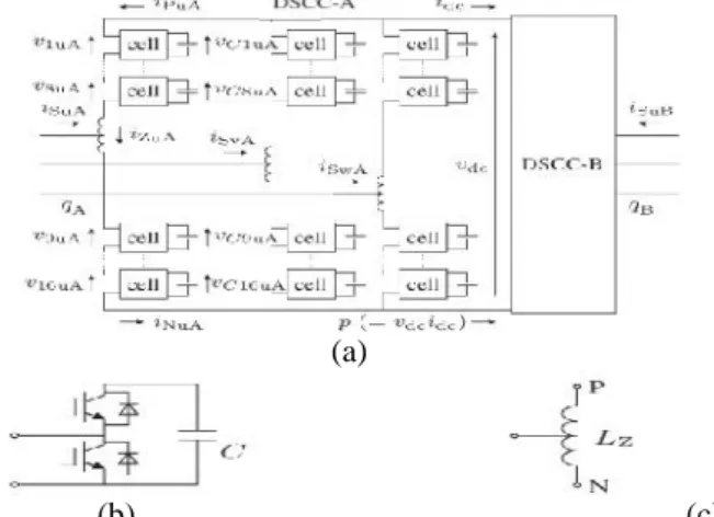
Fig. 2(a) shows the power circuit configuration of the Deceased BTB system with a per-leg chopper-cell count of 16.A couple of identical DSCCs, “DSCC-A” and “DSCC-B” are connected back-to-back without any common dc-link capacitor. Each DSCC consists of 48 chopper cells1depicted in Fig. 2(b), and three center-tapped inductors in Fig. 2(c). Here, LZ is not the inductance between the center tap and another node P or Nut the inductance between two nodes P and N. In Fig. 2(a), pica and inquire the positive and negative arm currents, is the supply current, and is the circulating current
(a)
(b) (c) Fig 2Circuit configuration of the DSCC-based BTB system with 16 chopper cells per leg. (a) Main circuit. (b) Chopper cell. (c) Center-tapped inductor.
Along the u-phase leg of DSCC-A. Reference [8] has made the definition of as follows:
=12( + ) (1)
The count of independent variables out of the three branch currents , inlay, and issue is not three but two because Kirchhoff’s current law comes into existence at the phase a terminal of DSCC-A or at the center tap of the u-phase center tapped inductor. Following [8], this paper selects the supply current and the circulating current as two independent variables. As a result, the positive and negative arm currents are expressed as dependent variables as follows:
The first terms of the right-hand sides in (2) and (3) are related to the supply current. They are out of phase by 180◦witheach other. As a result, the magnetic fluxes formed by the supply current cancel out each other inside the magnetic core of the center-tapped inductor. Therefore, the inductor presents no inductance to the supply current, whereas it renders the inductance LZ to the circulating current. Connected in parallel to make this experimental system effective as a downscaled BTB system. Fig. 3 shows the overview of the three-phase 200-V, 10-kW, and 50-Hz BTB system designed, constructed, and tested. Each a terminal of the two DSCCs is connected to the secondary side of a line-frequency transformer through an ac-link inductor Lac and a starting circuit. Each of the two line-frequency transformers with unity turns ratio is rated at 200 V, 15 kava, and 50 Hz. The leakage inductance of each transformer is much smaller tanoak, thus resulting in neglecting the effect of the leakage inductance. Each arm of the chopper cell consists of four power MOSFETs. The positive directions of idc and p are defined as the direction from DSCC-A to DSCC-B (left to right), as shown in Fig. 3.Moreover, qA and qB are three-phase instantaneous reactive (imaginary) powers with an engineering unit of [via] 2[19], [20] at the secondary sides of the two transformers. The values of qA and qB are defined as the positive (or negative) value when the DSCC acts as an inductor (or a capacitor).
Fig. 4 is a photo of the three-phase 200-V, 10-kW, and 50-HzBTB system designed and constructed for experiment. Table I summarizes the circuit parameters of Figs. 2 and 3, which are used in experiment and simulation. Each DSCC has16 chopper cells per leg. The dc reference voltage of each floating capacitor is set tov∗C=50V, so that the dc-link reference voltage should be set tov∗dc= 400V because of the existence of (21) in Section V-B. The reason why the BT system adopts the phase-shifted PWM technique presented in [8] will be described in Section IV-A. Each triangular-carrier frequency is set aft= 450Hz, and a dead or blanking times 8μs. Note that 16 triangular-carrier signals phase-shifted one another by22.5◦ (= 360◦/16). As described in Section II, the practical DSCC-based BT system rated at 200 MW has 88 chopper cells per leg. However, it would be unreasonable to construct a downscaled Deceased BTB system with a per-leg chopper-cell count of 88 forth purpose of confirming the reliability of experiment, simulation, and analysis. Therefore, the authors have intentionally increased each triangular-carrier frequency of the downscaled system to 450 Hz (slightly higher than that of the practical system), instead of decreasing the cascade count to 16. As result, the downscaled system is almost the same in equivalent triangular-carrier frequency as the practical system. Three phase nominal line-to-line rams voltages of 66 kV and 200 V in the practical and downscaled systems are typical high-voltage transmission and low-high-voltage distribution high-voltages in Japan, respectively.
The unit capacitance constant of the dc capacitors in Table I, His defined by
=32 (4)
The energy stored in all the dc capacitors, to which the rated voltage is applied, is divided by the rated power of the converter [21]. An SI unit offices [J]/ [W] = [s]. The unit capacitance constant is useful and effective in designing dc capacitors and in comparing dc capacitors in one BTB system to another one with different voltage and current ratings. The reason is that the unit capacitance constant can be considered as a kind of per-unit value although per-unit values have no physical unit.
IV CONTROL SYSTEM A. Phase-Shifted PWM Technique
A few different PWM techniques to create multilevel voltage waveforms would be applicable to a DSCC-based BTB system from a theoretical point of view [8], [22]–[25]. Among them,
Fig. 3. Overview of the three-phase 200-V, 10-kW, and 50-Hz downscaled BTB system with a unified digital controller.
Fig.4. Photo of the three-phase 200-V, 10-kW, 50-Hz BTB system used for experiment.
TABLE I
CIRCUIT PARAMETERS OF FIGS. 2 AND 3
Rated power P 10kw
Nominal line to line rms voltage
200v
Nominal line frequency
50Hz
Per-leg chopper cell count
n 16
Ac link inductor 2mH (16%)
Center-tapped inductor
3mH (24%)
Starting resistor R 20
DC-link reference voltage
∗ 400v
DC-capacitance reference voltage
∗ 50v
Dc capacitor C 6.6mF
Unit capacitance constant
40ms at 50v
PWM carrier frequency
450Hz
Equivalent carrier frequency
n 7.2kHz
This results in producing equal switching and conduction power losses in the individual chopper cells, making it simple and easy to design the heat-sink and/or cooling equipment of actual chopper cells. The phase-shifted PWM technique does not require the capacitor-voltage sorting and chopper-cell selecting processes presented in [2] but require the individual reference voltages of all the chopper cells for the individual balancing control inspection IV-C.
A. Three Sub controls
The control system for the DSCC-based BTB system shown in Figs. 2 and 3 can be classified into the following three sub controls based on feedback control: 1) Control of the active power and the reactive powers qA and qB at the secondary sides of the two transformers; 2) Control of the dc-link voltage and current (active power p, at the dc link);
3) Voltage control of all the floating dc capacitors. The power control is achieved on the−q synchronous reference frames in combination with decoupled current control. The dc-link voltage and current control will be described in Section V.
B. Voltage Control of All the DC Capacitors
The voltage control of all the floating dc capacitors is characterized by hierarchical control consisting of three layers [26].It is classified into the following three blocks: 1) Overall capacitor-voltage control;
2) arm-balancing control; 3) Individual balancing control.
The overall capacitor-voltage control in the top layer takes the responsibility for regulating the arithmetical average voltage of all the dc capacitors to its reference. Adjusting a small amount of active power supplied from the ac mains makes it
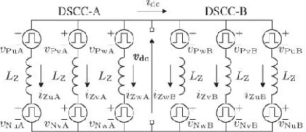
Fig. 5 Equivalent circuit for the DSCC-based BTB system in Fig. 2 with focus on the dc-link voltage and current
Possible to regulate the arithmetical average voltage of all the capacitors to its reference. Note that the adjusted active power corresponds to the whole power loss of the two DSCCs. This control results in producing a slight difference in active power between each ac side and the dc link.
The arm-balancing control in the middle layer plays an important role in balancing 12 arithmetical average voltages, each of which is the arithmetical average voltage of eight dc capacitors per arm. The dc component of the circulating current in each leg is adjusted to exchange a small amount of active power active-power difference between the positive and negative arms. This sophisticated controls the same in function as the cluster-balancing control used inane SSBC (single-star bridge cells)-based
STATCOM [27] and to the clustered SOC (state of charge)-balancing control used in an SSBC-based battery energy storage system (BESS) [28].However, the following essential difference exists: No circulating current flows in the SSBC whereas the circulating currents flowing in the DSCC can be controlled independently [1]. The individual balancing control in the bottom layer takes charge of regulating each dc-capacitor voltage to the arithmetical average voltage of eight dc capacitors per arm. This straightforward control adjusts the active power formed byte low-voltage-side voltage of each chopper cell and the arm current. The combination of the phase-shifted PWM technique with the voltage control of all the dc capacitors imposes no limitation on the number of cascaded chopper cells per leg theoretically.
V CONTROL OFDC-LINK VOLTAGE ANDCURRENT
This section provides an exclusive discussion on the dc-link voltage and current control, considering the two DSCCs as a unified power conversion system.
A. Equivalent Circuit and Basic Equations
Fig. 5 depicts an equivalent circuit for the DSCC-based BT system shown in Fig. 2, with focus on the dc-link voltage and current. A couple of three-phase ac circuits at the ac sides of the two DSCCs are removed from the equivalent circuit. The reasons are summarized as follows: 1) The supply current in each phase iS produces no effect on the voltage appearing between nodes P and N in the center-tapped inductor. This means that no magnetic flux is generated by the supply current because of the occurrence of cancellation as evident from (2) and (3), although a magnetic flux is generated by the circulating current. 2) The supply current in each phase produces no effect on the dc-link current because no zero-sequence current exists in a set of three-phase supply currents.
3) The chopped voltage at the low-voltage side of each chopper cell is determined by the duty factor and dc capacitor voltage of each chopper cell.
In addition, the stray inductance and resistance existing in each leg are neglected, and each center-tapped inductor is assumed as an ideal one without magnetic saturation or winding resistance.
Each arm of the two DSCCs in Fig. 2(a) is represented by the voltage source corresponding to the sum of the low-voltage-side voltages of the cascaded chopper cells per arm. For example,
The u-phase “collective” positive-arm and negative-arm voltages in DSCC-A, and , are given by
= (5)
=
/
(6)
= − =
, , , ,
(7)
The u-phase collective leg voltage is given by
= = + (8)
Kirchhoff’s voltage law is applicable to each leg, thus leading to the following equation:
= + (9)
Equations similar to (9) are valid for the other five legs. The following equations are obtained by adding the right-hand and left-hand sides of the equations related to all the three legs in the individual DSCCs and manipulating the resultant equations, along with (7)
=13
, ,
−13 (10)
=13
, ,
+13 (11)
From (10) and (11), and are given by
=16 (
, ,
+ ) (12)
=21 (
, ,
− ) (13)
Equation (12) means that is independent of , and that is equal to the arithmetical average of the six low-voltage side collective leg low-voltages in the BTB system. Equation (13) indicates that dice can be controlled by the voltage difference between the sum of the three collective leg voltages in DSCC-A and that in DSCC-B.
A. Control of DC-Link Voltage
Attention is paid to the u-phase leg in DSCC-A because of circuit symmetry in the three-phase circuit. The reference voltage at the low-voltage side of each chopper cell, ∗ can be divided into the following three terms:
∗ = ∗ ( ) + ∗ ( ) + ∗ (14) Here, ∗ (ac) is the ac (50-Hz) reference voltage; ∗ (dc) is the dc reference voltage, and ∗ is the control voltage of theca circulating current. Since the ac reference voltages in the positive arm are out of phase by 180◦with those in the negative arm, the following equation exists in ∗ ( ):
∗ ( ) = 0 (15)
Out of the three terms at the left-hand side of (14), ∗ ( )cannot be used to regulate the dc-link voltage or to control the dc-link current because it is the ac-terminal line-to-neutral reference voltage and devotes itself to controlling the supply current. On the other hand, ∗ ( )can be used to regulate theca-link voltage, as described in this subsection, while ∗ can be used to control the dc-link current, as discussed in the next subsection.
Equation (12) indicates that the following relation should exist between the references of the u-phase collective leg voltage, ∗ and the reference of the dc-link voltage, Vedic:
∗ = ∗ (16)
Hence, the dc reference voltage at the low-voltage side of each chopper cell, ∗ (dc) is given by
∗ ( ) = ∗ (17)
When ∗ = 0, the use of (5), (6), (8), and (14) together with (15) yields the following relation:
∗ = ∗ ( ) (18)
The arithmetical average voltage of the96 (= 16×6) dc capacitors in the BTB system, is given by
=61 ( +
, ,
). (19)
Note that does not contain the fundamental and second order harmonics because these harmonic components are cancelled out in each three-phase DSCC. The overall capacitor voltage control [26] adjusts the active powers delivered from the three-phase ac-mains voltages and to DSCC-An ands-B so that follows its reference ∗. The application of the decoupled control presented in [26] to the control system can avoid mutual interferences among the supply currents, theca current, the circulating currents, and the mean dc voltages of all the floating dc capacitors. Since ∗ ( ) is considered as a dc-biased voltage to
∗ ( ), (17) can be slightly modified into ∗ ( ) =
2 (20)
This equation relates the actual or detected high-voltage-side voltages of all the chopper cells in (19) to the actual clink voltage in (12), through the low-voltage-side dc reference voltages in (18). Then, taking (17) and (20) into consideration, the voltage reference of each dc capacitor, ∗ should be set as follows:
∗=2 ∗ (21)
The same equation as (21) exists in the other five legs. The detected and calculated dc voltage given by (19), vices regulated to its reference Vicky means of feedback control. As result, the dc-link voltage can be indirectly regulated to its reference ∗ without sensing the dc-link voltage as long as (20) is satisfied.3
In addition, the following advantage exists in the dc-link voltage control: The two DSCCs take the equal responsibility for regulating the dc-link voltage to its reference. To do it, each DSCC uses the common arithmetical-average voltage given by (19). Note that the average voltage is obtained from the two DSCCs with real-time communications.
C. Control of DC-Link Current
Controlling the dc-link current can is realized by controlling the circulating current flowing inside each leg. The reference of the dc-link current, ∗ is given by
∗ = ∗
/ (22)
Because of circuit symmetry, the u-phase reference circulating currents in DSCC-A and DSCC-B, ∗ and
∗ are assumed to be
∗ = − ∗ = − ∗
3 (23)
Equations similar to (23) are valid for the other v-phase and w-phase.
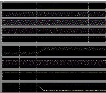
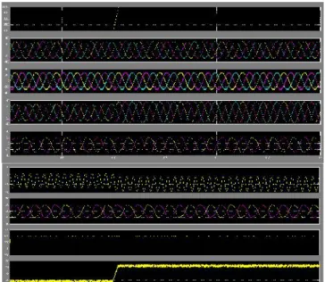
Fig.6. Experimental waveforms operating as a rectifier at ∗= 8.7 kW and ∗ =−5.0 kvai.
The following control voltage ∗Zia plays the leading role in constituting feedback control of the dc circulating current:
∗ = − ( ∗ − ) (24)
Where is the feedback gain. From (8), (14), (15) and (17), the reference of the u-phase collective leg voltage,
∗ is given by
∗ = ∗ + ∗ (25)
∗
, ,
= − ∗ , ,
= ( ∗ − ) (26)
Equations similar to (24) and (25) are valid for the other five legs. Note that the six reference circulating currents, included in (24) and its similar five equations, meet Kirchhoff’s current law because of the existence of (23). Moreover, it is clear that the six actual circulating currents also meet Kirchhoff’s current law. Equations (7) and (23) make it possible to change the control Voltage given by (24) into
= 2 ( ∗ − ∗ , ,
)
= (∗ − ) (27) A differential equation similar to (27) is valid for the circulating current in each leg. The two DSCCs take the equal responsibility for controlling the dc-link current to its reference. Equation (27) leads to the following conclusions. 1) the actual dc-link current exhibits a first-order response to a step change in its reference ∗ with a time constant owls/KZ.
2) Controlling is independent of regulating vice. D. Maximum DC-Link Ripple Voltage
This subsection assumes that the mean dc voltage of each chopper-cell capacitor is regulated toucan that the ac components of each capacitor are neglected. The use of a phase-shifted PWM technique makes voltage steps of and equal V∗C [10]. As a result, the instantaneous value of takes one out of ∗ , ∗ + ∗, and ∗ − ∗. This is valid for the other five legs. Equation (12), therefore, gives the following relation:
∗ − ∗≤ ≤ ∗ + ∗ (28)
Theoretically, the possible maximum ripples voltage appearing across the dc link is2V∗Cin peak-to-peak. Actually, the maximum ripple voltage would be lower than, or equal to, 2V∗C.
VI SIMULATION RESULTS
Fig. 7. Simulated waveforms operating as a rectifier atp∗= 8.7 kW andq∗A =−5.0 kvai.
Fig. 8. Simulated waveforms operating as an inverter atp∗= 8.7 kW andq∗B = 5.0 kvai.
Fig. 9. Simulated waveforms to a ramp change inp∗from 10-kW (rated)rectification to 10-kW inversion whereq∗A =
Fig. 10 Simulated waveforms to a small step change in active-power reference fromp∗= 8 to 10 kW whereq∗A =
q∗B = 0.
CONCLUSION
This paper has described a grid-level high-power BTB (back to-back) system using two modular multilevel cascade converters based on double-star chopper cells (MMCC-DSCC) without common dc-link capacitor. A three-phase 200-V,10-kW, 50-Hz BTB system with phase-shifted PWM has been designed, constructed, and tested to verify its operating principles and performance. Experimental and simulated waveforms have agreed well with each other not only in steady states but also in transient states. The simulation program developed in this paper is so reliable that it is applicable, particularly to investigations into low-voltage-ride-through (LVRT) capability and fault tolerances encountered in the operation of actual systems. Modeling and analysis have been done for the single power conversion system unifying the two DSCCs that take the equal responsibility for regulating the dc-link voltage and controlling the dc-link current. Concerning the transient response of theca-link current to a small step change in active-power reference from 8 to 10 kW, the time constant derived by analysis has been in a good agreement with those measured from both experiment and simulation. Experimental results have confirmed the effectiveness of a self-starting/restarting procedure.
REFERENCES
[1] H. Akagi, “Classification, terminology, and application of the Modular Multilevel Cascade Converter (MMCC),”
IEEE Trans. Power Electron., vol. 26, no. 11, pp. 3119– 3130, Nov. 2011.
[2] R. Marquardt and A. Lesnicar, “A new modular voltage source inverter topology,” inProc. EPE, 2003, pp. 2–4.
[3] S. Allebrod, R. Hamerski, and R. Marquardt, “New transformerless, scalable modular multilevel converters for HVDC-transmission,” inProc. IEEE PESC, 2008, pp. 174–
[4] R. Marquardt, “Modular multilevel converter: An universal concept for HVDC-networks and extended dc-bus-applications,” inProc. IPEC, 2010, pp. 502–507.
[5] J. Qin and M. Saeedifard, “Predictive control of a modular multilevel converter for a back-to-back HVDC system,”IEEE Trans. Power Del., vol. 27, no. 3, pp. 1538– 1547, Jul. 2012.
[6] M. Guan and Z. Xu, “Modeling and control of a modular multilevel converter-based HVDC system under unbalanced grid conditions,”IEEE Trans. Power Electron., vol. 27, no. 12, pp. 4858–4867, Dec. 2012.
[7] G. Bergnaet al., “An energy-based controller for HVDC modular multilevel converter in decoupled double synchronous reference frame for voltage oscillation reduction,” IEEE Trans. Ind. Electron., vol. 60, no. 6, pp. 2360–2371, Jun. 2013.
[8] M. Hagiwara and H. Akagi, “Control and experiment of pulsewidthmodulated modular multilevel converters,” IEEE Trans. Power Electron., vol. 24, no. 7, pp. 1737–1746, Jul. 2009.
[9] M. Hagiwara, K. Nishimura, and H. Akagi, “A medium-voltage motor drive with a modular multilevel PWM inverter,” IEEE Trans. Power Electron., vol. 25, no. 7, pp. 1786–1799, Jul. 2010.
[10] H. Peng, M. Hagiwara, and H. Akagi, “Modeling and analysis of switching-ripple voltage on the dc link between a diode rectifier and a modular multilevel cascade inverter (MMCI),”IEEE Trans. Power Electron., vol. 28, no. 1, pp. 75–84, Jan. 2013.
[11] M. Hagiwara, I. Hasegawa, and H. Akagi, “Start-up and low-speed operation of an adjustable-speed motor driven by a modular multilevel cascade inverter (MMCI),” IEEE Trans. Ind. Appl., vol. 49, no. 4, pp. 1556–1565, Jul./Aug. 2013.
[12] S. Rohner, J. Weber, and S. Bernet, “Continuous model of modular multilevel converter with experimental verification,” inProc. IEEE ECCE, 2011, pp. 4021–4028.
[13] J. Kolb, F. Kammerer, and M. Braun, “Straight forward vector control of the modular multilevel converter for feeding three-phase machines over their complete frequency range,” inProc. IEEE IECON, 2011, pp. 1596–1601.
[14] J. Kolb, F. Kammerer, and M. Braun, “Dimensioning and design of a modular multilevel converter for drive applications,” in Proc. EPE/PEMC, 2012, pp. LS1a-1.1-1– LS1a-1.1-8.
[16] L. Harnefors, A. Antonopoulos, S. Norrga, L. Angquist, and H.-P. Nee, “Dynamic analysis of modular multilevel converters,”IEEE Trans. Ind. Electron., vol. 60, no. 7, pp. 2526–2537, Jul. 2013.
[17] M. Saeedifard and R. Iravani, “Dynamic performance of a modular multilevel back-to-back HVDC system,”IEEE Trans. Power Del., vol. 25, no. 4, pp. 2903–2912, Oct. 2010.
[18] H.-J. Knaak, “Modular multilevel converters and HVDC/FACTS: A success story,” in Proc. IEEE EPE, 2011, pp. 1–6.
[19] H. Akagi, Y. Kanazawa, and A. Nabae, “Instantaneous reactive power compensators comprising switching devices without energy storage components,” IEEE Trans. Ind. Appl., vol. IA-20, no. 3, pp. 625–630, May/Jun. 1984.
[20] H. Akagi, E. H. Watanabe, and M. Aredes,
Instantaneous Power Theory and Applications to Power Conditioning. Piscataway, NJ, USA: IEEE Press, 2007.
[21] H. Fujita, S. Tominaga, and H. Akagi, “Analysis and design of a dc voltage-controlled static var compensator using quad-series voltagesource inverters,”IEEE Trans. Ind. Appl., vol. 32, no. 4, pp. 970–978, Jul./Aug. 1996.
[22] A. Antonopoulos, L. Angquist, and H.-P. Nee, “On dynamics and voltage control of the modular multilevel converter,” inProc. EPE, 2009, pp. 1–10.
[23] D. Siemaszko et al., “Evaluation of control and modulation methods for modular multilevel converters,” in
Proc. IPEC, 2010, pp. 746–753.
[24] S. Rohner, S. Bernet, M. Hiller, and R. Sommer, “Modulation, losses, and semiconductor requirements of modular multilevel converters,”IEEE Trans. Ind. Electron., vol. 57, no. 8, pp. 2633–2642, Aug. 2010.
[25] Q. Tu, Z. Xu, and L. Xu, “Reduced switching-frequency modulation and circulating current suppression for modular multilevel converters,” IEEE Trans. Power Del., vol. 26, no. 3, pp. 2009–2017, Jul. 2011.
[26] N. Niimura and H. Akagi, “Decoupled control of a three-phase modular multilevel cascade converter based on double-star chopper-cells,” (in Japanese), IEEJ Trans. Ind. Appl., vol. 132, no. 11, pp. 1055–1064, Nov. 2012.
[27] H. Akagi, S. Inoue, and T. Yoshii, “Control and performance of a transformerless cascade PWM STATCOM with star configuration,”IEEE Trans. Ind. Appl., vol. 43, no. 4, pp. 1041–1049, Jul./Aug. 2007.
[28] L. Maharjan, S. Inoue, H. Akagi, and J. Asakura, “State-of-charge (SOC)- balancing control of a battery energy storage system based on a cascade PWM converter,”