AUSTRALIAN JOURNAL OF BASIC AND
APPLIED SCIENCES
8414 -2309 : 8178 EISSN
-ISSN:1991
Journal home page: www.ajbasweb.com
Open Access Journal
Published BY AENSI Publication
© 2016 AENSI Publisher All rights reserved
This work is licensed under the Creative Commons Attribution International License (CC BY).
http://creativecommons.org/licenses/by/4.0/
To Cite This Article: Bushra A.Hasan, Jamal.M.Rzaij and Iftikhar .M.Ali., Sensing Properties of (In2O3:Eu) Thin Films. Aust. J. Basic & Appl. Sci., 10(8): 143-150, 2016
Sensing Properties of (In
2O
3:Eu) Thin Films
1Bushra A. Hasan, 2Jamal. M. Rzaij and 2Iftikhar. M. Ali
1University of Baghdad, College of Science, Department of Physics 2
University of Anbar, College of Science, Department of Physics
Address For Correspondence:
Bushra A.Hasan, University of Baghdad, College of Science, Department of Physics. E-mail:[email protected]
A R T I C L E I N F O A B S T R A C T Article history:
Received 12 February 2016 Accepted 18 March 2016 Available online 20 April 2016
Keywords:
Thin films of iridium doped indium oxide (In2O3:Eu)with different doping ratio(0,3,5,7,and 9%) are prepared on glass and single crystal silicon wafer substrates using spray pyrolysis method. The goal of this research is to investigate the effect of doping ratio on of the structural, optical and sensing properties . The structure of the prepared thin films was characterized at room temperature using X-ray diffraction. The results showed that all the undoped and doped (In2O3:Eu)samples are polycrystalline in structure and nearly stoichiometric. UV-visible spectrophotometer in the wavelength range (200-1100nm)was used to determine the optical energy gap and optical constants .The optical transmittance of 83% and the optical band gap of 5.2eV for pure In2O3 declare drastic reduction as Eu dopant introduce to the indium oxide and then return to increase with further increase of doping ratio. The best figure of merit of the films was achieved for pure sample.
INTRODUCTION
Non-stoichiometric transparent conducting oxides (TCO) such as tin oxide, cadmium oxide, zinc oxide, indium oxide, etc., find a wide variety of applications in microelectronic and optoelectronic devices because of their high optical transmittance in the visible range with high electrical conductivity. Among these, indium oxide In2O3 is an n-type degenerate semiconducting oxide which is finds optoelectronic applications such as flat panel displays,solar cells, photodiodes (Fortunato, E., 2007, Biyikli, N., 2001) .In2O3 is a wide-bandgap (3.75 eV) n-type semiconductor,with appreciable single-crystal mobility (160 cm2 V−1 s−1) and high film transparency in the visible region (> 90%) (Vygranenko, Y., 2007). For the past three decades many researchers have reported on the physical properties of In2O3 films formed by different deposition methods such as flash evaporation (Kaleemulla, S., 2007), electron beam evaporation (Subrahmanyam, A., U.K. Barik, 2005), dc/rf magnetron sputtering (Radhakrishna, B., 2000, Chen, L.C., S.C. Liu, 2006), laser deposition, molecular beam epitaxy (Huang, M.H., 2001), chemical vapor deposition (Bourlang, A., 2008, Prathap,2006), sol–gel process (Sailer, R.A., 2008), spray pyrolysis (Flores, M.A., 2008; Moholkar, A.V., 2008), electrochemical deposition (Ghimbeu, C.M., 2008) were employed for preparing indium oxide films to meet present day science and technological requirements. But less work has been reported on the influence of doping with Eu which affects the hole properties of In2O3 films prepared by spray pyrolysis method. The aim of this research is to determine the effect of doping ratio the structural, optical, and electrical properties of In2O3 thin films prepared at room temperature.
Basic Considerations:
these photons should have energy equal or greater than the energy gap of semiconductors. The absorption coefficient (α )which is the decrement ratio of incident radiation relative to unit length in the direction of wave propagation inside the medium is relating with the absorbance (A) through the relation (Klopffer , W., 1984):-
t
A
303
.
2
=
α
(1)Where (t) is the sample thickness. Many researchers (Ho, W.H., 2008; Tauc, J., 1974) put the empirical equation between the optical energy gap( Eg) and energy of the incident photon which is :-
(α hν) = A( hν -Eg)r (2)
Where A is constant, hν is the energy of incident photon which can be calculated using the equation:-
)
(
1240
nm
h
λ
ν
=
… (3)r is the order of the optical transition depending on the nature of electronic transition .The transition is called direct if the extremities of V.B and C.B lie at the same K-space ,while the transition is called indirect if the transition possible only with phonon assisted(
∆
k
≠
0
) (Pankov, J., 1971). Thus the value of (r) may be 1/2,2,3/2, and 3 corresponding to the allowed direct ,allowed indirect, forbidden direct and forbidden indirect transition recpectively.The absorption edge become wide for polycrystalline and amorphous semiconductors because of allowed localized states are found in the energy gap, the width of these localized states can be calculated using Urbach Rule (Korotcenkov, G., 2007)e
E
h
e
/
0
ν
α
α
=
(4)Where (α0 ) is constant and Ee is the width of localized states.
The optical behavior of materials utilized to determine its optical constants (refractive index (n), extinction coefficient (k), real and imaginary parts of dielectric constants ( ε1 , ε2 )). Several methods were proposed to determine the optical constants, they involve spectrophotometric measurements of reflectance (R) and transmittance (T) of sample in the wavelength range The extinction coefficient (imaginary part of the refractive index) can be calculated by the relation (Pankov, J., 1971):
π
αλ
4
=
k
…..(5)whereλ
is the wavelength ,α
is the absorption coefficient which can be obtained usingequation (1).
The refractive index (n) can be measured (when the reflectance (R) and (k) are known) by using the equation [22]:
)
1
(
)
1
(
)
1
(
4
2 2−
+
−
−
−
=
R
R
k
R
R
n
(6)The complex index (
N
) is given by:ε
=
−
=
n
ik
N
(7)Where ε is the complex dielectric constant, given by:
2
1
ε
ε
ε
=
−
i
(8)The parameter εr is the real part of dielectric constant , εi is the imaginary part of dielectric constant , from equations (9) and (10) one can obtained :
)
10
...(
...
...
...
...
...
...
...
...
...
...
2
)
9
..(
...
...
...
...
...
...
...
...
...
...
2 2nk
k
n
i r=
−
=
ε
ε
2. Experiments:In this work, In2O3 thin films were prepared on glass and single crystal silicon wafer P-Type (111) substrates using spray pyrolysis technique. The spray pyrolysis apparatus used in this work consists of a homemade spraying unit, a substrate holder with heater, and an enclosure. The glass substrate is kept on a stainless steel plate. The condition of preparation is listed in table below:
Spray Parameters Optimum Value/Item
Nozzle-Substrate Distance 30±2 cm
Spray Time 5 sec
Stopping Time 10 sec
Substrate Temperature 325 °C
Solution Flow Rate 2 ml/min
Carrier Gas O2
In2O3
0.1M
Eu 0.1M
Solvent
HCl
The structural aspects were investigated by X-ray diffraction (PW1840) using Cu Kα radiation. Optical
transmission for samples was measured with a UV-visible spectrophotometer Cary 100in the range 200-1100nm.
RESULTS AND DISCUSSION
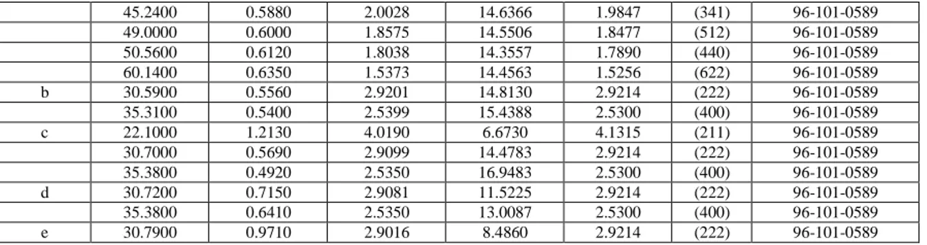
The XRD pattern of the undoped and Eu-doped In2O3 thin film prepared at different doping ratio deposited on glass substrate is shown in Fig. 1. The results show that the as deposited In2O3films was polycrystalline in nature,by increasing the doping ratio the films exhibit a polycrystalline structure with (222) being the dominant orientation. The introduction of iridium to the host prepared films has significant effect on the structure i.e. the crystallinity of the films was worsened , hence the grain size was reduced. The average grain size (particle size) D of the thin films was calculated using the Scherer equation (Korotcenkov, G., 2007): D = 0.94λ/(β cosθ),where λ is the X-ray wavelength, β is the full-width at half-maximum of the (222) diffraction line and θ is the diffraction angle of the XRD spectra. All of the diffraction peaks can be indexed to the cubic In2O3 (JCPDS card no. 96-101-0589. No peaks corresponding to Eu are observed, indicating that iridium gets incorporated well into the In2O3 lattice. The reduction in the grain size attributed to increase in the density of the grain boundaries. By further increase in the doping ratio, the XRD spectrum tend to approach amorphous structure (Parthibab, S., 2009).The intensity ratio of the peaks (222) orientation decreases along with the doping ratio. By increasing the doping ratio from 0 to 9%, the grain size decreased from 14.5 nm to 8.48 nm and this is in good agreement with the optical data which is found in Table.2. The particle size is found to be 14.5, 14.8, 14.47,11.5 and 8.48 nm at the doping ratio of 0, 3,5,7and 9% respectively. It can be observed that the crystallite sizes decreases on elevating the doping ratio because the doping decreases the energy of ions or ion clusters prior to collision with the substrates(Jeong,S.H.,2003).
Fig. 1: XRD patterns of In2O3:Eu thin films doped with different doping ratio(a) In2O3 , (b) In2O3 doped with 3% Eu,(c) In2O3 doped with 5% Eu ,(d)In2O3 doped with 7% Eu,(e)In2O3 doped with 9% Eu .
Table 1: Effect of Eu doping on XRD results of the In2O3 thin films.
Sample 2θ (Deg.) FWHM
(Deg.) dhkl Exp.(Å) G.S (nm) dhkl Std.(Å) hkl card No.
21.2000 0.5650 4.1875 14.3048 4.1315 (211) 96-101-0589
27.4800 0.6120 3.2431 13.3633 3.2002 (301) 96-101-0589
30.2200 0.5650 2.9550 14.5642 2.9214 (222) 96-101-0589
a 32.8000 0.6350 2.7283 13.0413 2.7047 (231) 96-101-0589
35.1400 0.5650 2.5518 14.7487 2.5300 (400) 96-101-0589
45.2400 0.5880 2.0028 14.6366 1.9847 (341) 96-101-0589
49.0000 0.6000 1.8575 14.5506 1.8477 (512) 96-101-0589
50.5600 0.6120 1.8038 14.3557 1.7890 (440) 96-101-0589
60.1400 0.6350 1.5373 14.4563 1.5256 (622) 96-101-0589
b 30.5900 0.5560 2.9201 14.8130 2.9214 (222) 96-101-0589
35.3100 0.5400 2.5399 15.4388 2.5300 (400) 96-101-0589
c 22.1000 1.2130 4.0190 6.6730 4.1315 (211) 96-101-0589
30.7000 0.5690 2.9099 14.4783 2.9214 (222) 96-101-0589
35.3800 0.4920 2.5350 16.9483 2.5300 (400) 96-101-0589
d 30.7200 0.7150 2.9081 11.5225 2.9214 (222) 96-101-0589
35.3800 0.6410 2.5350 13.0087 2.5300 (400) 96-101-0589
e 30.7900 0.9710 2.9016 8.4860 2.9214 (222) 96-101-0589
Figure 2 shows the optical transmittance curves as a function of wavelength for the In2O3:Eu thin films that are prepared with different doping. It is clear form the figure that the average transmittance of the thin films is more than 85% for wavelengths in the 500–1100 nm range, indicating the good transparency of the thin films. Moreover, it can be seen that the optical transmittance observed in the films decreases with the increase of doping ration in the first but then increase with continues increase of doping ratio, indeed the transmittance decreases from 85% to 22% with an increase in the doping ratio from 0 to 5% and then return to increase to 32%with further increase of doping ratio. Furthermore, high transmittance in the films may be ascribed to less scattering effects, structural homogeneity and better crystallinity. A red-shift in the absorption edge was observed as iridium added to the hot material. Note worthy the red-shift of the cut-off edge take place as a result of reduction in to grain size, arises from doping(Green,L.E.,2003). This may be attributed to the creation of the defect states in the gap or the strain . With the increase of doping ratio from 5 to 9%, there is UV-off shifts to shorter wavelength which is accompanied by increase of band gap as can be seen later, this is known as the Burstein–Moss shift.
0 20 40 60 80 100
200 300 400 500 600λ (nm)700 800 900 1000 1100
T
ra
n
sm
it
ta
n
ce
%
Pure In2O3 Doped with 3% Eu Doped with 5%Eu Doped with7%Eu Doped with 9%Eu
Fig. 2: Transmittance spectra for the Eu-doped In2O3 thin films obtained at different doping ratio.
The refractive index (n) of undoped and Eu doped In2O3films with different doping ratio were measured
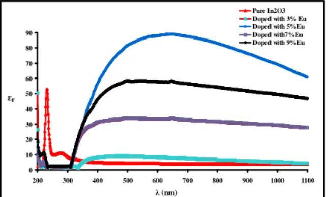
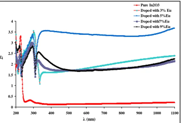
and plotted as function of wavelength (λ) in Fig .3.It was found that(n)decreased with (λ) in the range (200-1100) nm,on the other hand at λ=500nm which lies in middle of spectrum of the transparent region, the refractive index exhibit to change in non systematic sequence with doping ratio i.e. increases in the first and then decreases with further increase of doping ratio, indeed n increases from ( 2.08 to 9.01 ) with increasing of doping ratio from 0 to 5% and then return to decrease when Eu ratio increases to 9%. indicating that the increasing of doping ratio made the samples films more opaque to the incident light in the first but then return be more transparent to the incident light. The dependence of the extinction coefficient (k) on the wavelength is shown in Fig.4. It is evident that the values of (k) were reduced, become smaller at the region beyond the absorption edge, they are relatively small with increasing of (λ).It is remarked that (k) values at λ=500nm increased from (0.082 to 0.284 as Eu introduced to the host material but then k decreases with further increase of Eu .The increasing of k can be attributed to the increasing of absorption coefficient ,hence k will be increased according to equation (5), while the decreasing of k is ascribes to eliminating of defect states responsible about the absorption processes in the band gap. Real and imaginary parts of dielectric constant (ε1 and ε2 ) of undoped
and Eu doped In2O3films with different doping ratio were calculated using equs.( 9 and 10 ). The dependence of
(εr) and (εi ) on (λ) are shown in Figs.(5) and (6) ,it is concluded that the variation of (εr) mainly depend on the value of (n2) because the smaller value of (k) comparison with (n2) ,while the imaginary part of dielectric constant (εi ) mainly depend on (k) values which are related to the variation of (α ).
The variation of (α hν)2 (α hν)1/2 with photon energy (hν) for direct and indirect allowed transition are plotted in Fig.7 and 8 for undoped and Eu doped In2O3films with different doping ratio , the optical energy gaps
are determined which are listed is Table.1. It is clear that direct (Eg)decreases as Eu added to In2O3 films ,
when Eu ratio increase from 0 to 3%nm, while (Eg) increases to 3.5 eV as Eu ratio increases to 9% .Also the indirect energy gap show the same sequence with doping ratio , notworthy the indirect band gap values are lower than those direct bangap values . The drastic decrease in the energy gap at 3% doping ratio is related that this sample attain maximum particle size (14.8nm) as seen from table.1 .The optical bandgaps obtained for doped films are much lower than that of undoped one. The reduction of the bandgap is in good agreement with the red shift observed from transmittance spectra due to the Burstein–Moss effect .
0 1 2 3 4 5 6 7 8 9 10
200 300 400 500 600 700 800 900 1000 1100
λ (nm) n
Pure In2O3 Doped with 3% Eu Doped with 5%Eu Doped with7%Eu Doped with 9%Eu
Fig. 3: Variation of refractive index with the wavelength for the Eu-doped In2O3 thin films obtained at different doping ratio.
0 0.2 0.4 0.6 0.8 1 1.2
200 300 400 500 600 λ (nm)700 800 900 1000 1100
k
Pure In2O3 Doped with 3% Eu Doped with 5%Eu Doped with7%Eu Doped with 9%Eu
Fig. 4: Variation of extinction coefficient k with wavelength for the Eu-doped In2O3 thin films obtained at different doping ratio.
0 10 20 30 40 50 60 70 80 90
200 300 400 500 600 700 800 900 1000 1100
λ (nm)
εr
Pure In2O3 Doped with 3% Eu Doped with 5%Eu Doped with7%Eu Doped with 9%Eu
Fig. 5: Variation of εr with the wavelength for the Eu-doped In2O3 thin films obtained at different doping ratio.
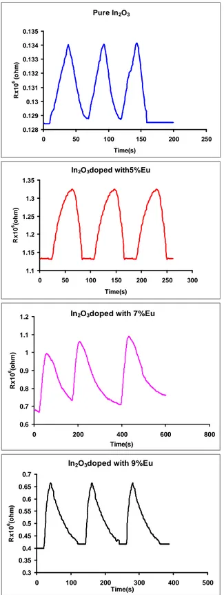
The electrical properties were determined. In this work, the gas sensing properties of the In2O3:Eu thin films which are deposited by spray pyrolysis technique was characterized for NO2. The sensitivity, (S) of the film is
defined as the ratio between the surface resistance of the film in air (Ra) and gas (Rg):
)
(
)
(
Ω
Ω
=
gas air
R
R
S
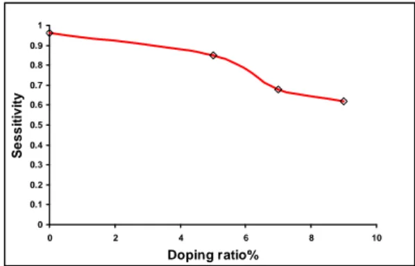
Generally, films with higher resistance declared a greater response to the reducing ambient gas . This behavior indicates direct correlation between the gas response and the film stoichiometry.Generally, when the conductivity (resistivity) is low (high), the response to the reducing gases is high. According to XRD results (Fig.1), the undpoed sample which shows lower deviation of stoichiometry compared to the residual samples, hence, as expected better sensitivity was observed for the pure sample as shown in Fig.(10).
0 0.5 1 1.5 2 2.5 3 3.5 4
200 300 400 500 600 700 800 900 1000 1100
λ (nm)
εi
Pure In2O3 Doped with 3% Eu Doped with 5%Eu Doped with7%Eu Doped with 9%Eu
Fig. 6: Variation of εi with the wavelength for the Eu-doped In2O3 thin films obtained at different doping ratio.
0 10 20 30
0 1 2 3 4 5 6
hν (eV)
(
α
h
ν
)
2(c
m
-2.
(e
V
)
2)*
1
0
1
0
Pure In2O3 Doped with 3% Eu Doped with 5%Eu Doped with7%Eu Doped with 9%Eu
Fig. 7: Variation of (αhυ)2 versus (hυ)for the Eu-doped In2O3 thin films obtained at different doping ratio.
0 100 200 300 400 500 600 700 800 900 1000
0 1 2 3 4 5 6
hν (eV)
(
α
h
ν
)
1
/2
(c
m
-1
/2.
(e
V
)
1
/2)
Pure In2O3 Doped with 5%Eu Doped with 9%Eu Doped with7%Eu Doped with 3% Eu
Fig. 8: Variation of (αhυ)1/2 versus (hυ)for the Eu-doped In2O3 thin films obtained at different doping ratio.
Table 2: The optical parameters of In2O3:Eu thin films .
Sample T% α (cm-1) k n εr εi Eg
(eV)direct
Eg (eV)indirect
Pure In2O3 85.30 7951 0.032 2.086 4.352 4.352 5.20 4.9
Doped with 3%Eu 54.45 69908 0.284 2.995 8.889 8.889 3.18 3.2
Doped with 5%Eu 22.03 48018 0.191 9.019 81.307 81.307 3.20 3.26
Doped with 7%Eu 39.33 36963 0.147 5.819 33.837 33.837 3.50 3.40
Pure In2O3
0.128 0.129 0.13 0.131 0.132 0.133 0.134 0.135
0 50 100 150 200 250
Time(s)
R
x
1
0
6 (
o
h
m
)
In2O3doped with5%Eu
1.1 1.15 1.2 1.25 1.3 1.35
0 50 100 150 200 250 300
Time(s)
R
x
1
0
6(o
h
m
)
In2O3doped with 7%Eu
0.6 0.7 0.8 0.9 1 1.1 1.2
0 200 400 600 800
Time(s)
R
x
1
0
6 (o
h
m
)
In2O3doped with 9%Eu
0.3 0.35 0.4 0.45 0.5 0.55 0.6 0.65 0.7
0 100 200 300 400 500
Time(s)
R
x
1
0
6(o
h
m
)
Fig. 9: The dynamic response versus recovery time cycle for for In2O3:Eu thin films sensors.
Conclusions:
analysis reveals that the gas sensitivity is higher for pure samples which contains both higher surface roughness and electrical resistivity.
0 0.1 0.2 0.3 0.4 0.5 0.6 0.7 0.8 0.9 1
0 2 4 6 8 10
Doping ratio%
S
e
s
s
it
iv
it
y
Fig. 10: Sensitivity versus doping ratio for In2O3:Eu thin films sensors.
REFERENCES
Fortunato, E., D. Ginley, H. Hosono, D.C. Paine, 2007. Mater. Res. Soc. Bull, 32: 242. Hara, K., K. Sayama, H. Arakawa, 2000. Solar Energy Mater. Solar Cells, 62: 441.
Biyikli, N., T. Kartgoglu, O. Aytur, I. Kimukin, E. Ozbay, 2001. Appl. Phys. Lett, 79: 2838. Vygranenko, Y., K. Wang, A. Nathan, 2007. Appl. Phys. Lett., 91: 263508.
Wang, L., M.H. Yoon, G. Lu, Y. Yang, A. Facchetti, T.J. Marks, 2006. Nat. Mater, 5: 893. Dixit, A., C. Sudakar, R. Naik, V.M. Naik, G. Lawes, 2009. Appl. Phys. Lett, 95: 192105
Kaleemulla, S., A. Sivasankar Reddy, S. Uthanna, P. Sreedhara Reddy, 2007. Mater. Lett, 61: 4309. Subrahmanyam, A., U.K. Barik, 2005. J. Phys. Chem. Solids, 66: 817.
Radhakrishna, B., T.K. Subramanyam, B. Srinivasulu Naidu, S. Uthanna, 2000. Opt. Mater, 15: 217. Subrahmanyam, A., U.K. Barik, 2006. J. Phys. Chem. Solids, 67: 1518.
Chen, L.C., S.C. Liu, 2006. Solid State Electron, 50: 1355.
Huang, M.H., Y. Wu, H. Feick, N. Tran, E. Weber, P. Yang, 2001. Adv. Mater, 13: 113.
Bourlang, A., D.J. Payne, R.G. Egdell, J.S. Foord, P.P. Edwards, M.O. Jones, A. Schertel, P.J. Dobson, J.L. Hutchison, 2008. Appl. Phys. Lett, 92: 092117.
Prathap, P., Y.P. Venkata Subbaiah, M. Devika, K.T. Ramakrishana Reddy, 2006. J.Mater. Chem. Phys., 100-375.
Sailer, R.A., A.Wanger, C. Schmit, N. Klaverkamp, D.L. Schulz, 2008. Surf. Coat. Technol, 203-835. Flores, M.A., R. Castanedo, G. Torres, J. Marquez, O. Zelaya, 2008. Thin Solid Films, 570- 681.
Moholkar, A.V., C.M. Pawar, K.Y. Rajpure, V. Ganesan, C.H. Bhosale, J. Alloys, 2008. Compd, 464-387. Ghimbeu, C.M., J. Schoonman, M. Lumbreras, 2008. Ceram. Int., 34-95.
Klopffer , W., 1984." Introduction to Polymer Spectroscopy",Springer – Verlag. Ho, W.H., C.F. Li, H.C. Liu, S.K. Yen, 2008. J. Power Sources, 175-897. Tauc, J., 1974. Amorphous and Liquid Semiconductors, Plenum Press. Pankov, J., 1971. Optical Process in Semiconductors, London.
Korotcenkov, G., M. Nazarov, M.V. Zamoryanskaya, M. Ivanov, 2007. Thin Solid Films, 515: 8065. Rozati, S.M., T. Ganj, 2004. Renew. Energy, 29: 1665. [http://dx.doi.org/10.1016/j.renene.2004.01.007]. Parthibab, S. V. Gokulakrishnan, K. Ramamurthi, E. Elangovan, R. Martins, E. Fortunato, R. Ganenan, 2009.Solar Energy Mater. Solar Cells, 93-92.
Jeong S.H., S. Kho, D. Jung, S.B. Lee, J.H. Boo, 2003. Deposition of aluminum-doped zinc oxide films by RF magnetron sputtering and study of their surface characteristics, Surface and Coatings Technology, 174–175: 187–192.
Greene, L.E., M. Law, J. Goldberger, F. Kim, J.C. Johnson, Y. Zhang, R.J. Saykally and P. Yang, 2003. Angew. Chem. Int. Ed., 42: 3031 [http://dx.doi.org/10.1002/anie.200351461].
Burstein, E., 1952. Phys. Rev., 93: 632.
Mott and Davis, 1979. Electronic Process in Non Crystalline Semiconductors, 2nd edition, University Press. Oxford.
Korotcenkov, G., V. Brinzari, A. Cerneavschi, M. Ivanov, V. Golovanov, A. Cornet, J. Morante, A. Cabot, J. Arbiol, 2004. Thin Solid Films, 460-315 [http://dx.doi.org/10.1016/j.tsf.2004.02.01