Quantification of re-absorption and re-emission
processes to determine photon recycling efficiency
in perovskite single crystals
Yanjun Fang
1, Haotong Wei
1, Qingfeng Dong
1& Jinsong Huang
1Photon recycling, that is, iterative self-absorption and re-emission by the photoactive layer itself, has been speculated to contribute to the high open-circuit voltage in several types of high efficiency solar cells. For organic–inorganic halide perovskites that have yielded highly efficient photovoltaic devices, however, it remains unclear whether the photon recycling effect is significant enough to improve solar cell efficiency. Here we quantitatively evaluate the re-absorption and re-emission processes to determine photon recycling efficiency in hybrid perovskite with its single crystals by measuring the ratio of the re-emitted photons to the initially excited photons, which is realized by modulating their polarization to differentiate them. The photon recycling efficiencies are revealed to be less than 0.5% in CH3NH3PbI3and
CH3NH3PbBr3 single crystals under excitation intensity close to one sun, highlighting the
intrinsically long carrier recombination lifetime instead of the photon-recycling-induced photon propagation as the origin of their long carrier diffusion length.
DOI: 10.1038/ncomms14417
1Department of Mechanical and Materials Engineering, University of Nebraska-Lincoln, Lincoln, Nebraska 68588, USA. Correspondence and requests for
T
he power conversion efficiency (PCE) of organic–inorganic halide perovskite (OIHP)-based solar cells has skyrocketed from 3.8% to a certified 22.1% in less than six years1–18. This is already higher than that of the commercial multi-crystalline Si solar cells and is approaching that of single crystal ones. One contribution of the high PCE of OIHP solar cells is from its small open-circuit voltage (VOC) deficiency, that is,(Eg–eVOC)/e, where Eg is the optical band gap, and e is the
elementary charge. We have demonstrated that by mitigating the energy disorder in the organic electron transport layer via solvent annealing, the VOC deficiency of planar-structured
CH3NH3PbI3(MAPbI3) perovskite solar cells can be reduced to
as low as 0.42 V. Bi et al.19 also reported that by optimizing the composition of the perovskite layer to enhance the electroluminescence yield of the solar cells, the VOCof the best
device with a PCE of 20.8% can reach 1.15 V. This corresponds to a VOC deficiency of 0.40 V, which is much lower than that
of organic solar cells and is comparable to those of copper indium gallium selenide (CIGS) and single crystal Si solar cells20. However, the presentVOCdeficiency in OIHP solar cells is
still larger than that of the best GaAs solar cells, which is around 0.30 V, while in the latter case it was proposed that the photon recycling effect contributes to the highVOC. So a hypothesis that
naturally arises is that the photon recycling effect may also exist in OIHP materials giving rise to high VOC in perovskite solar
cells. There are two kinds of definitions of photon recycling in literature21,22. One only considers one-cycle of photon re-absorption, which refers to the radiatively emitted photons after external light excitation can be absorbed again by the photoactive layer itself. In this case, the photon recycling efficiency is the ratio of re-absorbed photons versus the total emitted photons. As shown in Fig. 1(a), for a 1 mm thick CH3NH3PbBr3 (MAPbBr3) single crystal, most of the
photoluminescence (PL) spectrum falls in its own absorption spectrum, leading to a re-absorption ratio of 94.2% calculated by dividing the integrated intensity of the self-filtered PL by that of the original PL. The other definition considers the multiple cycles of photon re-emission and re-absorption processes, and thus the way to characterize the photon-recycling efficiency is to measure the final emission intensity after multiple cycles. As a result of the repeated re-absorption and re-emission processes, the photon recycling effect allows the building up of charge carriers in the active layer to increase the quasi-Fermi-level splitting23,24. Since we are more concerned on whether the photon-recycling effect is strong enough to impact the VOC of
perovskite solar cells, we focused on the measurement of emission intensity after multiple cycles of re-absorption and re-emission.
Materials with high photon recycling efficiency generally meet two criteria: (1) large overlapping of its PL spectrum with the absorption spectrum, that is, the materials should have a small Stokes shift or even an anti-Stokes shift, so that the self-absorption of light can be efficient; and (2) a high-internal PL quantum yield (higher than 80% for GaAs under strong illumination intensity of 100 sun)25,26. As demonstrated above, the re-absorption probability is very high in MAPbBr3 single crystals. Yamada
et al.27 also observed a similar re-absorption phenomenon in
MAPbI3single crystals from a two-photon PL measurement. Such
a large self-absorption ratio in perovskite materials meets the prerequisite for efficient photon recycling. It should be noted that the Stokes shift is usually positive for perovskite thin film, that is, the emission peak is red-shifted compared with the absorption edge28. The overlapping of the absorption curve and PL emission curve for a thick perovskite single crystal is purely a thickness effect, as thicker perovskite can absorb more band tail light, leading to a gradual red-shift of the absorption edge with the increase in perovskite thickness. Moreover, a high-PL quantum yield above
90% has been reported in some OIHP nanomaterials, which, however, does not make efficient solar cells because of a poor charge transport property29.
The photon recycling scenario was further promoted by the observation of unique double PL peaks in the PL spectra of many perovskite single crystals of different compositions30, despite the additional lower energy peak also assigned to the emission of excitons bound to the surface defects31or the excess PbBr2 (ref. 32). Recently, Pazos-Outo´n et al.22 first reported
experimental evidence for the photon recycling effect in lead triiodide perovskite polycrystalline thin films being that charge generation was observed in a region longer than 50mm away from the light absorbing region. Though this length has not reached the reported longest carrier diffusion length in single crystal perovskite22,33, it is far beyond the diffusion length of polycrystalline films along the lateral direction where a lot of grain boundaries present.
In this study, we quantify the photon recycling effect in perovskite materials with their single crystals by directly measuring its efficiency. The origin of the double peaks in the PL spectra of a variety of perovskite single crystals is also investigated to determine whether they are caused by the photon recycling effect. The photon recycling efficiency in perovskite single crystals is quantitatively evaluated by measuring the ratio of the re-emitted photons to the incident exciting photons, which are differentiated from each other by modulating their polarization. The results reveal that the photon recycling
efficiency is below 0.5% in both MAPbBr3 and MAPbI3
single crystals under light excitation intensity close to one sun, which excludes its contribution to carrier transport in perovskite single crystals.
Results
Quantifying the photon recycling efficiency. We directly measured the photon recycling efficiency in perovskite single crystals based on the mechanism schematically shown in Fig. 1(b). After PL is generated on the top surface of a single crystal by the short wavelength light excitation, half of the PL emission transmits through the crystal and is filtered by the crystal itself. In addition, during its transmission, the high-energy portion of the PL is absorbed by the crystal itself, which yields re-emission with the PL peak shifting with respect to the absorption edge defined by the Stokes shift. Therefore, PL emitting out from the bottom of the crystal may be composed of both the filtered PL (PLF), and PL generated by multiple cycles
of self-absorption and re-emission, that is, recycled PL (PLR).
By measuring the ratio of PLR and PLF with respect to the
total transmitted PL (PLT), one can determine the photon
recycling efficiency in the single crystals.
the polarization of PL from SC1 by a linear polarizer (P1), we expected it to retain this polarization after transmission through SC2. In contrast, the recycled PL was assumed to be nonpolarized. Therefore, these two types of PL could be readily differentiated from each other by a second linear polarizer (P2) with a perpendicular polarization direction to P1 (P1>P2), which was expected to completely block thePLFwhile transmitting 50%PLR.
If there was emission of a large amount of photons after re-absorption, we expected to see a similar shape and intensity of the P1||P2 spectrum and P1>P2 spectrum, as schematically shown in Supplementary Fig. 1(a). In contrast, if the intensity of the P1>P2 spectrum was much smaller than that of the P1||P2 spectrum (Supplementary Fig. 1(b)), it would indicate that only a small amount of photons were re-emitted after re-absorption and, hence, a low photon recycling efficiency.
It was found that the optical birefringence of the MAPbBr3
single crystal could slightly change the polarization of the transmitted light, which was evidenced by its polarized microscopy image34. Therefore,PLFcannot be crossed out up to
the polarizer’s light extinction limit (0.05%). The transmission light spectrum for P1>P2 is actually the sum of PLR and
unblocked PLF. So the PLF that has not been crossed out
after transmission through P2 needs to be subtracted to more accurately determine PLR, which can be measured with
the setup schematically shown in Fig. 1(d). Specifically, the emission of a 650 nm light emitting diode (LED), whose photon energy is far below the band gap of MAPbBr3, was used to
replace the PL from SC1 to pass SC2. Since the below-bandgap light was not expected to induce the photon recycling effect in perovskite single crystals, the intensity ratio of the optical
PL generated at surface
Excitation light
Normalized PL or transmittance (a.u.) 1.2
1.0
0.8
0.6 0.4
0.2
0.0 MAPbBr3 single crystal
MAPbBr3
single crystal 2 (SC2)
Polarizer 2 (P2)
Photomasks
Photomasks
Transmitted light (IT)
Polarizer 2 (P2) Polarizer 1 (P1)
650 nm LED
Birefringence induced unblocked light (IB)
MAPbBr3
single crystal 1 (SC1)
MAPbBr3
single crystal 405 nm laser
450 nm long-pass filter Incident PL
(PLI)
Polarizer 1 (P1)
Recycled PL (PLR)
Filtered PL (PLF)
Recycled PL (PLR)
Wavelength (nm) Transmitted PL
Transmittance PL
500 550 600 650 700
PLR
PLF
a b
c
d
Figure 1 | Scheme of the photon recycling measurement method.(a) Normalized photoluminescence (PL) spectrum of a 1 mm thick CH3NH3PbBr3
(MAPbBr3) single crystal (SC) measured with photomask (red curve), its normalized transmission spectrum (green curve), and the calculated transmitted
birefringence-induced unblocked light (IB) to the light
transmitted through the single crystal (IT) represents the
portion of the unblocked PLF.
We first verified that the polarization of PL from SC1 after transmitting through P1 was linearly polarized. As shown in Supplementary Fig. 2, the polarized PL emission from SC1 after transmission through P1 was almost completely blocked by the P2 (P1>P2), for a blocking ratio of about 99.95% which represents the upper limit for the polarizers used. Also, the polarization of the PL emission from SC2 was investigated with both the reflection and transmission mode measurements. In the reflection mode, the PL excitation and detection were on the same side of the single crystals; while for the transmission mode, the PL detection was on the opposite side of the crystals with the excitation, as schematically shown in Supplementary Fig. 3(a) and 4(a), respectively. The corresponding PL spectra shown in Supplementary Fig. 3(b) and 4(b), proved that the PL emission from SC2 was nonpolarized, despite the excitation light being 100% polarized. Therefore, half of PLRcan transmit
through P2, as shown in Fig. 1(c).
We measured the spectra ofPLRand PLTof a 1.3 mm thick
MAPbBr3 single crystal to determine its photon recycling
efficiency by adjusting the polarization direction of P1 and P2 to be P1>P2 or P1||P2, respectively. The MAPbBr3 single
crystals used for the measurements were grown from solution by a modified antisolvent crystallization method34,35, and the high quality of these crystals was evidenced by excellent transparency, a record high mobility lifetime product, and the high sensitivity of the X-ray detectors made from them, as previously reported by us34. To improve the surface quality of the single crystals, a ultraviolet-ozone treatment was performed on them for 10 min, which has been proven to reduce surface recombination velocity to be comparable with the best
passivated silicon34. As shown in Fig. 2(a), only the long wavelength tail of the incident PL (PLI) from SC1 transmitted
through the SC2, regardless of the polarization direction of P2. The integrated intensity of PLT is about 4.7% of that of
PLI, corresponding to a large re-absorption ratio of 95.3%.
The integrated PL intensity for P1>P2 was only 0.40% of that of PLT (Fig. 2b), indicating most of the transmitted PL was
contributed by the filtered PL. The portion of unblocked PLF induced by the birefringence effect, which needs to be
subtracted from thePLRspectrum, can be obtained based on the
IB/ITratio when using the emission of a 650 nm LED to penetrate
the single crystal (Fig. 2c). It was noted that only the photons of PLRemitted within the critical solid angle (escape cone,O) can
escape the crystal through the bottom surface, which was calculated to be 0.3pbased on the refractive index of MAPbBr3
(n¼1.9) (ref. 36) and air (n¼1) and assuming an isotropic emission of PLR. The light out-coupling ratio ofPLRwas thus
calculated to be 7.5%. So the actual integrated intensity ratio (Z) of recycled PL to incident PL, or the photon recycling efficiency, was calculated to be 0.48% based on the equation below:
Z¼O 2PLR
4pPLIð1RÞ
ð1Þ
where R is the reflectance of the single crystal surface, and the ratio was multiplied by a constant of 2, because only half of PLR can transmit through P2. We have also measured
the photon recycling efficiency of several other pieces of MAPbBr3 single crystals with different thicknesses, and all
of them exhibited a low efficiency below 0.5%, despite of a high re-absorption probability larger than 70%, as summarized in Supplementary Fig. 5 and Fig. 2(d). The above results indicate that the photon recycling effect is insignificant in MAPbBr3single crystals under one sun excitation.
PLI
500 550 600 650 700
500 550 600 650 700 500 550 600 650 700
IT
IB
1
PL intensity (a.u.)
Light intensity (a.u.)
10–1
10–2
10–3
10–4
10
10–1
10–2
10–3
10–4
100
PL intensity (a.u.)
10–1
10–2
10–3
10
Photon recycling efficiency
1E–4 0.01
1E–3
Wavelength (nm)
Wavelength (nm) Wavelength (nm)
Under 650 nm LED illumination
MAPbBr3 SCs with
various thicknesses
Crystal thickness (mm) 0.1
P1 ⊥ P2 P1 || P2
P1 || P2
c d
Figure 2 | Photon recycling efficiency in MAPbBr3single crystals (SCs).(a)PLI(blue curve) andPLT(black curve) spectra of a 1.3 mm thick MAPbBr3
single crystal showing its PL self-absorption ratio, wherePLIrepresents the incident PL from SC1 shown in Fig. 1(c), andPLTis measured by adjusting the polarization direction of P1 and P2 in Fig. 1(c) to be parallel with each other; (b)PLTandPLRspectra showing the PL re-emission ratio, wherePLRis measured by adjusting the polarization direction of P1 and P2 in Fig. 1(c) to be perpendicular with each other; (c) The spectra of the 1.3 mm thick MAPbBr3
SCs excited by a 650 nm LED whose photon energy is far below the band gap of MAPbBr3, and measured with the polarization direction of P1 and P2 in
The photon recycling efficiency of a MAPbI3 single crystal
has also been investigated by the same method. We chose MAPbI3 single crystals of two representative thicknesses for the
measurement. One was a 3 mm thick single crystal that was demonstrated to possess the ultralong carrier recombination lifetime33,37, and the other was a thinner single crystal with a thickness of 52mm. As shown in Supplementary Fig. 6, the blocking ratio of PL from MAPbI3SC1 was only 98.1% after
transmission through two polarizers with perpendicular polarization directions, which was limited by the light extin-ction ratio of the near infrared (NIR) polarizers used here. Figure 3a,b shows that the integrated intensity ratio of the PLR to PLI was much larger than that of the MAPbBr3
single crystals. However, from the IB to IT intensity ratio
excited by light with energy far below the band gap of MAPbI3
(Fig. 3c), one can find that the high PLR/PLI intensity ratio
mainly originated from the birefringence-effect-induced unblocked PLF. After subtracting this portion, and also taking
into account the light extraction ratio, the calculated photon recycling efficiency was 0.47 and 0.51% for the 3 mm and 52mm thick single crystals, respectively (Fig. 3d). This is comparable to that of the MAPbBr3single crystals, indicating
a low photon recycling efficiency in the MAPbI3single crystals.
Origin of double peaks in photoluminescence spectrum. Another question which needs to be answered is what is the origin of the double PL peaks that are observed in a variety of perovskite single crystals. We measured the PL spectrum of MAPbBr3 single crystals with both the reflection mode and
transmission mode and with the measurement geometry schematically shown in Fig. 4(a), so that we could distinguish the transited and scattered fluorescence. Figure 4(b) shows a typical PL spectrum of a 1 mm thick MAPbBr3 single crystal excited
by a 405 nm laser measured in the reflection mode., which shows a small shoulder at around 570 nm (Peak 2) with the main peak at 538 nm (Peak 1). However, when a photomask was applied on the excitation surface of the crystal to block the emission from areas surrounding the excitation spot and from the crystal edges (Fig. 4(a)), Peak 2 was significantly suppressed (Fig. 4(b)). The PL spectrum of the same crystal under the transmission mode showed only one peak with the same peak position as Peak 2 (Fig. 4(b)). Since the PL captured in the transmission mode mainly consisted of the PL transmitting through the whole crystals, it underwent self-absorption; and hence only the long wavelength emission emitted out of the crystal, as shown in Fig. 1(a). Based on the above results, it was concluded that the double peak observed in the PL reflection mode was a combination of the PL generated on the top surface (Peak 1), as well as the filtered PL leaking out from the top surface and edge of the crystal after self-absorption and multiple reflection (Peak 2). This result excludes the origin of the photon recycling effect as the origin of Peak 2.
To verify the origin of these two peaks, we measured the temperature-dependent PL spectra of the MAPbBr3single crystal
from 89 K to 290 K under the reflection mode without applying the photomask (Supplementary Fig. 7) and the temperature-dependent integrated PL intensity of Peak 1 and Peak 2 were fitted by the equation below to derive their activation energies (Ea):38
IðTÞ ¼ I0
1þAekEBaT
ð2Þ
where I(T) is the PL intensity at temperature T, I0 is the
PL intensity at 0 K, kB is the Boltzmann constant, and A is a
fitting parameter. As shown in Fig. 4(c), both fittedEaof Peaks 1
and 2 were around 59 meV, indicating the same origin of the two peaks, instead of from the free and bound exciton emissions, respectively. To further confirm that Peak 2 was from reflection/ scattering of the PL generated on the crystal surface, we dip coated
0 5 10 15 20 25 30
52 μm MAPbI3 SC
3.0 mm MAPbI3 SC
P1 || P2
P1 || P2
P1 ⊥ P2 P1 ⊥ P2
PLI
PLI
PL intensity (a.u.)
10–1
10–2
10–3
10–4
100
PL intensity (a.u.)
10–1
10–2
10–3
10–4
100
IB
/
IT
(%)
0.01
1E–3
Photon recycling efficiency
Wavelength (nm)
1
925 950 975 1,000 0.01 0.1 10
Crystal thickness (mm) Wavelength (nm)
900 850 800 750
700 700 750 800 850 900
Wavelength (nm)
Under below band gap light illumination
MAPbI3 SCs with
various thicknesses
3 mm MAPbI3 SC
52 μm MAPbI3 SC
a b
c d
Figure 3 | Photon recycling efficiency in CH3NH3PbI3(MAPbI3) single crystals.(a,b)PLT(black curve), andPLR(red curve) spectra of a 3 mm thick
(a) and a 52mm thick (b) MAPbI3single crystal (SC) measured by adjusting the polarization direction of P1 and P2 in Fig. 1(c) to be parallel or
perpendicular with each other, respectively; The blue curve is thePLIspectrum; (c) TheIBtoITintensity ratio of the 52mm (red symbol) and the 3 mm thick (blue symbol) single crystals, excited by light with energy far below the band gap of MAPbI3in order to determine the contribution from the optical
a thick [6,6]-phenyl-C61-butyric acid methyl ester (PCBM) layer on the bottom of the crystals and measured the PL in the reflection mode without applying a photomask, as schematically shown in the inset of Fig. 4(d). We speculate that the coated PCBM eliminated the light reflection at the bottom surface by absorbing the PL. As expected, Peak 2 disappeared after coating with PCBM, both at room temperature and low temperature (77 K), as shown in Fig. 4(d). The disappearance of Peak 2 at low temperature also ruled out the possibility that Peak 2 originated from the defects-induced bound excitons because the relative intensity of the bound exciton peak in the PL spectrum was expected to be stronger at lower temperature.
Discussion
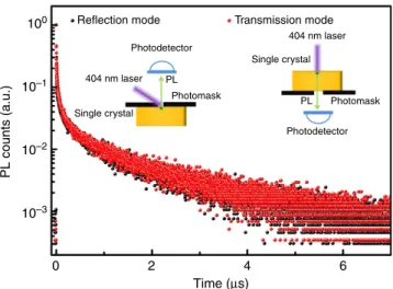
One of the direct consequences of the photon recycling effect was the elongation of the carrier radiative recombination lifetime because of the multiple cycles of regeneration of charge carriers by self-absorption39. We measured the radiative carrier recombination lifetime of a 3 mm thick high quality MAPbBr3
single crystal grown by a modified antisolvent crystallization method, which we recently demonstrated to show improved crystal quality and hence further increased sensitivity of X-ray detectors made of them (unpublished). This further verified the low photon recycling efficiency demonstrated above. The measurement was carried out both under reflection mode and transmission mode and with the application of a photomask. The PL measured under the reflection mode with a photomask mainly came from the crystal surface, while the PL measured under the transmission mode included both the filtered surface PL and the photon recycling PL. So if the photon recycling efficiency was high in the perovskite single crystals, the PL lifetime measured
under the transmission mode would be much longer than that measured under the reflection mode. Since the PL lifetime of perovskite materials was wavelength dependent40, while the PL spectra measured under the reflection mode and transmission mode were quite different from each other, a 568 nm band-pass filter with a 10 nm band width was placed in front of the detector to restrict the detection wavelength range to be identical for these two measurement modes. As shown in Fig. 5, the PL decay measured under the reflection mode exhibited a fast decay within the first 100 ns, followed by slow recombination dynamics with a decay time constant of about 1.2ms. The fast decay component may come from the carrier inward diffusion because of the high carrier mobility of single crystals27. Carrier recombination near the surface region may also have contributed to this decay process, while the slow component was generally assigned to the bulk recombination. The long decay time constant indicated the high quality of the single crystals. The PL decay curve measured under transmission mode almost overlapped with that measured with the reflection mode. This clearly indicates that the PL measured under the transmission mode was mainly from the surface-generated PL filtered by the crystal itself instead of the photon recycling PL. Hence its decay dynamics generally followed the trend of the surface PL decay process, which further confirmed that the photon recycling effect is not significant in these perovskite single crystals.
The low photon recycling efficiency of perovskite materials might be caused by its low PL quantum yield, which is reported to be highly dependent on excitation light intensity and is below 20% under one sun illumination at room temperature22,41,42. The light-intensity-dependent PL quantum efficiency was reported to be caused by a spin-split indirect-gap of perovskite material based on an ab initio relativistic calculation result.
Normalized PL intensity (a.u.)
Normalized PL intensity (a.u.)
Integrated PL intensity (a.u.)
1.0
0.8
0.6
0.4
0.2
0.0
1.0
0.8
0.6
0.4
0.2
0.0 Excitation light
Excitation light
Excitation light Single crystal
Single crystal
Single crystal
PL peak 2
PL peak 1
PL peak 2
Photomask (M) Photomask
PL peak 1
Wavelength (nm)
500 550 600 650 700
1/T (K–1)
Peak 1
7×10⁵
6×10⁵
5×10⁵ 4×10⁵
3×10⁵
2×10⁵
1×10⁵
0
Peak 2
Ea1 = 58.6 meV
Ea2 = 59.7 meV
0.004 0.006 0.008 0.010 0.012
Wavelength (nm)
Excitation light
Single crystal
PCBM PL peak 1 As-grown SC With PCBM 300K With PCBM 77K
500 550 600 650 700
Peak 1
Peak 2
R mode w/o M R mode with M T mode
d c
Figure 4 | Origin of double peak in the PL spectrum of MAPbBr3single crystals.(a) Schematic diagram of the PL measurement modes: reflection mode
(left panel) and transmission mode (right panel); (b) Normalized PL spectra of a 1 mm thick MAPbBr3single crystal (SC) measured under the reflection
mode without photomask (black curve) or with photomask (red curve), and under the transmission mode (blue curve); The peak wavelength of the PL measured under the transmission mode matches that of the long wavelength peak (peak 2) measured under the reflection mode without photomask, as marked by the green dashed line; (c) Temperature dependent integrated PL intensity of peaks 1 and 2 shown inb; The red curves are the typical fitting of the data by equation (2) to determine their activation energies (Ea1andEa2); (d) Normalized PL spectra of a MAPbBr3single crystal measured under the
Its calculated radiative recombination rate was more than two orders of magnitude lower than that of GaAs and CdTe under one sun illumination43. Surface passivation of perovskite thin films could dramatically enhance the PL lifetime to be close to the intrinsic lifetime of single crystals44. However, the PL quantum yield of these passivated films with a PL lifetime longer than 8ms was only 35%, which is still too low for efficient photon recycling. Future research is still needed to fully passivate the defects in perovskite materials for photon recycling purposes. The low-photon recycling efficiency demonstrated in perovs-kite single crystals also indicates that their long carrier diffusion length, reported previously, is indeed because of other factors, such as its intrinsically high-carrier recombination lifetime, instead of the iterative absorption and re-emission process that increases the carrier transport distance. In fact, the ultralong carrier recombination lifetime of MAPbI3single crystal has been
verified by the time-resolved microwave conductivity technique37. During this measurement, the charge carriers are excited by light with a penetration depth comparable to the crystal thickness, so that the contribution from the photon recycling effect to the carrier lifetime is negligible.
Regarding the contribution of the photon recycling effect to the VOC of perovskite solar cells, it is well known that the photon
recycling effect can increase theVOCof a solar cell by elongating
the carrier recombination lifetime. Generally, the influence of carrier recombination lifetime on theVOCcan be estimated by the
following equations:
VOC¼
nidkBT
q lnð
JSC
J0
þ1Þ ð3Þ
J01¼q
ffiffiffiffiffiffi
Dp
tp
s
n2
i
ND
þ
ffiffiffiffiffiffi
Dn
tn
r
n2
i
NA
!
ð4Þ
J02¼q
niW
2teff
ð5Þ
J0¼J01þJ02 ð6Þ
where JSC is short circuit current, J0 is the reverse saturation
current,nid is the diode ideal factor,J01is the diffusion-induced
reverse saturation current, Dp,nare the diffusivity of holes and
electrons, respectively, tp,n are the carrier lifetime of holes and
electrons, respectively, ND, A are the donor and acceptor
concentrations, respectively,niis the intrinsic carrier
concentra-tion,J02is the recombination induced reverse saturation current,
W is the depletion layer width, and teff is the effective
recombination lifetime, or directly measured lifetime. Since the ideal factor for the perovskite solar cells is close to 2, we expect theJ02will dominate the reverse saturation current and assume
J0¼J02. The maximum photon recycling efficiency of 0.5% we
measured in perovskite single crystals translates into an increase in the radiative recombination lifetime of only 0.5%. The corresponding VOC increment was calculated to be only about
0.26 mV if the initial VOC was assumed to be 1.1 V, which
is basically in agreement with the measured no-change of PL recombination lifetime. For the current most emissive photovoltaic material, GaAs, it is reported that the radiative recombination lifetime could be increased by 4–6 times as a result of photon recycling45, which corresponds to a photon recycling efficiency of between 75 and 83%. However, its contribution to the VOCenhancement in GaAs solar cells is still small. Even
for the best GaAs solar cell, the open-circuit voltage increment as a result of photon recycling is only 4 meV under 1 sun condition46, probably because of the overwhelming nonradiative recombination in the current high-efficiency solar cells under operating conditions.
Note that the photon recycling efficiency measurement reported here was performed on perovskite single crystals rather than the polycrystalline thin films which are widely used in current high efficiency perovskite solar cells. It is not feasible to use it for photon recycling efficiency measurement, because the film thickness in polycrystalline solar cells is comparable to the light attenuation length, and thus re-emission/re-absorption does not occur as much in the out-of-plane direction. Never-theless, since photon recycling in thin film devices refers to the light transport along the in-plane direction and/or across the film after multiple instances of reflection/scattering by the surface22, the light recycling across the single crystal is similar to thin film devices, from geometry aspects. On the other hand, the single crystals may exhibit a different PL property in comparison to the polycrystalline thin films, which means that the measurement results here cannot exclude the strong photon recycling efficiency in polycrystalline films. For instance, it was reported that the PL in CsPbBr3 might come from defects47, which could explain
lower PL quantum efficiency in CsPbBr3single crystals. Besides,
the quicker carrier diffusion in single crystal samples as compared with polycrystalline thin films may also result in a lower PL quantum efficiency. However, we did not see obviously weaker PL from the MAPbBr3 single crystals as compared with
the polycrystalline films, and the difference in reported results may be caused by an unawareness of the sensitivity of MAPbBr3
to environmental gases48. The perovskite grain size in the high-efficiency polycrystalline films was already over ten times larger than the exciton Bohr radius in these materials49, and thus the optical property of polycrystalline films approached that of the single crystals, though the photon recycling efficiency in polycrystalline films still needs to be determined by other independent characterization. Nevertheless, our results should still be relevant to the perovskite single-crystal-based solar cells, which have recently drawn increased research attention50,51 and may achieve comparable or better efficiency than the polycrystalline thin film based ones because of the orders of magnitude smaller trap density in single crystals. Finally, even if the photon recycling efficiency of perovskite polycrystalline thin
10–3 10–2 10–1 100
PL counts (a.u.)
Time (μs)
0 2 4 6
Reflection mode Transmission mode
404 nm laser
404 nm laser
Single crystal
Single crystal
Photomask Photomask
PL PL
Photodetector Photodetector
Figure 5 | Time-resolved PL decay of a high quality MAPbBr3single crystal.The time-resolved PL decay curves of a 3 mm thick high quality MAPbBr3single crystal (SC) measured under reflection mode with
its contribution to the VOC enhancement would still not be
significant with the present dominating device structures. The electron and hole transport layers always quench the PL from the perovskite films at a faster rate than PL emission, which results in a very low internal PL quantum yield. So the high VOCof perovskite solar cells is mainly attributed to other factors,
such as the unique defect-tolerant properties of perovskite materials52. In order to utilize the photon recycling effect to further increase the VOC of perovskite solar cells, the
nonquenching selective electrodes need to be explored to realize the high internal PL quantum yield and hence a high internal light intensity.
In summary, the photon recycling effect in perovskite single crystals was quantitatively evaluated by measuring the ratio of the recycled photons to the initially excited photons based on their polarization difference, which exhibited a low photon recycling efficiency o0.5% under one sun excitation intensity. The origin of the unique double peaks in the PL spectra of perovskite single crystals has been investigated in detail. It has been shown that the additional lower energy peak mainly comes from the filtered PL leaking out from the top surface and edge of the crystal after self-absorption and multiple reflections. The results presented here confirm that the long carrier diffusion length of perovskite single crystals previously reported is not facilitated by the photon recycling-induced photon propagation, highlighting their intrinsically excellent charge transport property.
Methods
Material synthesis.The MAPbBr3thick single crystals were grown by the
anti-solvent crystallization method34, and the MAPbI3thick single crystals were
grown by the top-seeded solution growth method33. The MAPbBr3and MAPbI3
thin single crystals with thickness equal oro100mm were grown from an ultrathin geometry-confined system53.
Optical characterization.The transmission spectrum of the single crystals was recorded with a LAMBDA 1050 ultraviolet/vis/NIR spectrophotometer (PerkinElmer) equipped with an integrating sphere. The photoluminescence measurements were carried out on a Horiba 320 photoluminescence system with a 405 nm or 532 nm laser as the excitation light source. The temperature dependent PL measurement was performed in a temperature controlled probe stage with liquid nitrogen as the coolant. The polarization of the PL from MAPbBr3
single crystals was modulated with visible polarizers, while that from MAPbI3
single crystals was modulated with NIR polarizers. The time-resolved PL was measured with a Horiba DeltaPro time-correlated single photon counting system, and the 404 nm pulsed laser diode with pulse width of 45 ps was used as the excitation source. The scattered laser was eliminated with a 450 nm long-pass filter. And a 568 nm band-pass filter with band width of 10 nm was used to select the detection wavelength range.
Data availability.The authors declare that the data that support the findings of this study are available from the corresponding author on reasonable request.
References
1. Kojima, A., Teshima, K., Shirai, Y. & Miyasaka, T. Organometal halide perovskites as visible-light sensitizers for photovoltaic cells.J. Am. Chem. Soc.
131,6050–6051 (2009).
2. Zhou, H.et al.Interface engineering of highly efficient perovskite solar cells. Science345,542–546 (2014).
3. Yang, W. S.et al.High-performance photovoltaic perovskite layers fabricated through intramolecular exchange.Science348,1234–1237 (2015).
4. Stranks, S. D.et al.Electron-hole diffusion lengths exceeding 1 micrometer in an organometal trihalide perovskite absorber.Science342,341–344 (2013). 5. Mei, A.et al.A hole-conductor–free, fully printable mesoscopic perovskite solar
cell with high stability.Science345,295–298 (2014).
6. Chen, W.et al.Efficient and stable large-area perovskite solar cells with inorganic charge extraction layers.Science350,944–948 (2015). 7. Liu, M., Johnston, M. B. & Snaith, H. J. Efficient planar heterojunction
perovskite solar cells by vapour deposition.Nature501,395–398 (2013). 8. Jeon, N. J.et al.Compositional engineering of perovskite materials for
high-performance solar cells.Nature517,476–480 (2015).
9. Burschka, J.et al.Sequential deposition as a route to high-performance perovskite-sensitized solar cells.Nature499,316–319 (2013). 10. Liu, D. & Kelly, T. L. Perovskite solar cells with a planar heterojunction
structure prepared using room-temperature solution processing techniques. Nat. Photon.8,133–138 (2014).
11. Lin, Q., Armin, A., Nagiri, R. C. R., Burn, P. L. & Meredith, P. Electro-optics of perovskite solar cells.Nat. Photon.9,106–112 (2015).
12. Im, J.-H., Jang, I.-H., Pellet, N., Gra¨tzel, M. & Park, N.-G. Growth of CH3NH3PbI3 cuboids with controlled size for high-efficiency perovskite solar cells.Nat. Nano9,927–932 (2014).
13. Jeon, N. J.et al.Solvent engineering for high-performance inorganic–organic hybrid perovskite solar cells.Nat. Mater.13,897–903 (2014).
14. Bi, C.et al.Non-wetting surface-driven high-aspect-ratio crystalline grain growth for efficient hybrid perovskite solar cells.Nat. Commun.6,7747 ð2015Þ:
15. Xiao, Z.et al.Efficient, high yield perovskite photovoltaic devices grown by interdiffusion of solution-processed precursor stacking layers.Energy Environ. Sci.7,2619–2623 (2014).
16. Wang, Q.et al.Large fill-factor bilayer iodine perovskite solar cells fabricated by a low-temperature solution-process.Energy Environ. Sci.7,2359–2365 (2014).
17. Dong, Q.et al.Abnormal crystal growth in CH3NH3PbI3-xClx using a multi-cycle solution coating process.Energy Environ. Sci.8,2464–2470 (2015).
18. Best research-cell efficiency. http://www.nrel.gov/pv/assets/images/efficiency_ chart.jpg (2016).
19. Bi, D.et al.Efficient luminescent solar cells based on tailored mixed-cation perovskites.Sci. Adv.2,e1501170 (2016).
20. Green, M. A., Emery, K., Hishikawa, Y., Warta, W. & Dunlop, E. D. Solar cell efficiency tables (version 46).Prog. Photovolt. Res. Appl.23,805–812 (2015).
21. Bensaid, B., Raymond, F., Leroux, M., Ve`rie´, C. & Fofana, B. Influence of luminescence self-absorption on photoluminescence decay in GaAs.J. Appl. Phys.66,5542–5548 (1989).
22. Pazos-Outo´n, L. M.et al.Photon recycling in lead iodide perovskite solar cells. Science351,1430–1433 (2016).
23. Walker, A. W.et al.Impact of photon recycling on GaAs solar cell designs. IEEE J. Photovoit5,1636–1645 (2015).
24. Yablonovitch, E. Lead halides join the top optoelectronic league.Science351,
1401–1401 (2016).
25. Nelson, R. J. & Sobers, R. G. Minority-carrier lifetimes and internal quantum efficiency of surface-free GaAs.J. Appl. Phys.49,6103–6108 (1978). 26. Schnitzer, I., Yablonovitch, E., Caneau, C. & Gmitter, T. J. Ultrahigh
spontaneous emission quantum efficiency, 99.7% internally and 72% externally, from AlGaAs/GaAs/AlGaAs double heterostructures.Appl. Phys. Lett.62,
131–133 (1993).
27. Yamada, Y.et al.Dynamic optical properties of CH3NH3PbI3 single crystals as revealed by one- and two-photon excited photoluminescence measurements. J. Am. Chem. Soc.137,10456–10459 (2015).
28. Zhang, W.et al.Ultrasmooth organic–inorganic perovskite thin-film formation and crystallization for efficient planar heterojunction solar cells.Nat. Commun.
6,6142 (2015).
29. Huang, H., Susha, A. S., Kershaw, S. V., Hung, T. F. & Rogach, A. L. Control of emission color of high quantum yield CH3NH3PbBr3 perovskite quantum dots by precipitation temperature.Adv. Sci.2,1500194 (2015).
30. Fang, Y., Dong, Q., Shao, Y., Yuan, Y. & Huang, J. Highly narrowband perovskite single-crystal photodetectors enabled by surface-charge recombination.Nat. Photon.9,679–686 (2015).
31. Priante, D.et al.The recombination mechanisms leading to amplified spontaneous emission at the true-green wavelength in CH3NH3PbBr3 perovskites.Appl. Phys. Lett.106,081902 (2015).
32. Fang, X.et al.Effect of excess PbBr2 on photoluminescence spectra of CH3NH3PbBr3 perovskite particles at room temperature.Appl. Phys. Lett.108,
071109 (2016).
33. Dong, Q.et al.Electron-hole diffusion lengths4175mm in solution-grown CH3NH3PbI3 single crystals.Science347,967–970 (2015).
34. Wei, H.et al.Sensitive x-ray detectors made of methylammonium-lead tribromide perovskite single crystals.Nat. Photon.10,333–339 (2016). 35. Shi, D.et al.Low trap-state density and long carrier diffusion in organolead
trihalide perovskite single crystals.Science347,519–522 (2015). 36. Alias, M. S.et al.Focused-ion beam patterning of organolead trihalide
perovskite for subwavelength grating nanophotonic applications.J. Vac. Sci Technol. B33,051207 (2015).
37. Bi, Y.et al.Charge carrier lifetimes exceeding 15ms in methylammonium lead iodide single crystals.J. Phys. Chem. Lett.7,923–928 (2016).
39. Asbeck, P. Self-absorption effects on the radiative lifetime in GaAs-GaAlAs double heterostructures.J. Appl. Phys.48,820–822 (1977).
40. He, H.et al.Exciton localization in solution-processed organolead trihalide perovskites.Nat. Commun.7,10896 (2016).
41. Stranks, S. D.et al.Recombination kinetics in organic-inorganic perovskites: excitons, free charge, and subgap states.Phys. Rev. Appl.2,034007 (2014). 42. Sutter-Fella, C. M.et al.High photoluminescence quantum yield in band gap
tunable bromide containing mixed halide perovskites.Nano Lett.16,800–806 (2016).
43. Azarhoosh, P., McKechnie, S., Frost, J. M., Walsh, A. & van Schilfgaarde, M. Research update: relativistic origin of slow electron-hole recombination in hybrid halide perovskite solar cells.APL Mater.4,091501 (2016). 44. deQuilettes, D. W.et al.Photoluminescence lifetimes exceeding 8ms and
quantum yields exceeding 30% in hybrid perovskite thin films by ligand passivation.ACS Energy Lett.1,438–444 (2016).
45. Ahrenkiel, R. K.et al.Ultralong minority-carrier lifetime epitaxial GaAs by photon recycling.Appl. Phys. Lett.55,1088–1090 (1989).
46. Braun, A., Katz, E. A., Feuermann, D., Kayes, B. M. & Gordon, J. M. Photovoltaic performance enhancement by external recycling of photon emission.Energy Environ. Sci.6,1499–1503 (2013).
47. Stoumpos, C. C. & Kanatzidis, M. G. The renaissance of halide perovskites and their evolution as emerging semiconductors.Acc. Chem. Res.48,2791–2802 (2015).
48. Fang, H.-H.et al.Ultrahigh sensitivity of methylammonium lead tribromide perovskite single crystals to environmental gases.Sci. Adv.2,e1600534 (2016). 49. Grancini, G.et al.Role of microstructure in the electron–hole interaction of
hybrid lead halide perovskites.Nat. Photon.9,695–701 (2015).
50. Dong, Q.et al.Lateral-structure single-crystal hybrid perovskite solar cells via piezoelectric poling.Adv. Mater.28,2816–2821 (2016).
51. Peng, W.et al.Solution-grown monocrystalline hybrid perovskite films for hole-transporter-free solar cells.Adv. Mater.28,3383–3390 (2016). 52. Yin, W.-J., Shi, T. & Yan, Y. Unusual defect physics in CH3NH3PbI3
perovskite solar cell absorber.Appl. Phys. Lett.104,063903 (2014). 53. Liu, Y.et al.Thinness- and shape-controlled growth for ultrathin
single-crystalline perovskite wafers for mass production of superior photoelectronic devices.Adv. Mater.28,9204–9209 (2016).
Acknowledgements
We thank the financial support from the National Science Foundation under award of OIA-1538893.
Author contributions
J.H. conceived this project. J.H. and Y.F. designed the experiments. Y.F. carried out the PL measurements. H.W. and Q.D. synthesized the perovskite single crystals. J.H. and Y.F. analysed the data and wrote the manuscript.
Additional information
Supplementary Informationaccompanies this paper at http://www.nature.com/
naturecommunications
Competing financial interests:The authors declare no competing financial interests.
Reprints and permissioninformation is available online at http://npg.nature.com/ reprintsandpermissions/
How to cite this article: Fang, Y.et al.Quantification of re-absorption and re-emission processes to determine photon recycling efficiency in perovskite single crystals.
Nat. Commun.8, 14417 doi: 10.1038/ncomms14417 (2017).
Publisher’s note: Springer Nature remains neutral with regard to jurisdictional claims in published maps and institutional affiliations.
This work is licensed under a Creative Commons Attribution 4.0 International License. The images or other third party material in this article are included in the article’s Creative Commons license, unless indicated otherwise in the credit line; if the material is not included under the Creative Commons license, users will need to obtain permission from the license holder to reproduce the material. To view a copy of this license, visit http://creativecommons.org/licenses/by/4.0/