Automatic Fuzzy Control Design for Parallel DC-DC Converters
Rong-Jong Wai, MEMBER,IAENG,and Yi-Chang Chen
Abstract−This study mainly focuses on the development of
an automatic fuzzy control (AFC) system for a parallel dc-dc converter, and the control objective is to achieve the stable voltage regulation and uniform current distribution. The average model for an example of a three-module boost converter, which is composed of three conventional boost converter frames in parallel connection, is derived for the design of this AFC system including voltage and current control loops. In the voltage control loop, the target of the inductor current is designed to be followed by the current control loop, and the current control loop is designed via incremental fuzzy form to control respective duty ratios. In this AFC scheme, the fuzzy inference mechanism is automatically built according to inherent circuit properties without complex tuning algorithms or computation processes. The effectiveness of the proposed control scheme is verified by numerical simulations, and the advantages of good transient response and robustness to uncertainties are indicated in comparison with a conventional proportional-integral control (PIC) system.
Index Terms−Automatic fuzzy control, Stable voltage
regulation, Uniform current distribution, Parallel dc-dc converter, Boost converter.
I. INTRODUCTION
Nowadays, parallel dc-dc converters with fundamental boost mechanism and large power capacity have been widely used in many industrial applications for promoting the level of low-voltage-type sources and satisfying ever
demanding power requirements [1]−[3]. With this
arrangement, it offers efficient processing of built-in redundancy and ensures the supply of high output currents in applications such as mainframe computers, systems using very large scale integration (VLSI) technology, and uninterruptible power supplies (UPS) [3]. Control of the fundamental boost converter frame in parallel dc-dc converters is a challenging problem because, besides being a bilinear system (with a binary input in its exact description, or a saturated one in the average model) it is also a non-minimum phase system with respect to the output to be controlled [4], [5]. The existence of unstable zero dynamics introduces a hard constraints on the achievable performance [5]. Being a nonlinear system, a parallel-connected system of boost converters may behave in many ways that could not be manipulated by conventional linear design and analytic methods. In order to improve system reliability and reducing current stress on switching devices, the control objective must ensure the
equal sharing of the load current among parallel converters and the stable regulation of the output voltage [3].
Traditionally, conventional proportional-integral-
derivative (PID)-type controllers are widely used in
industry due to their simple control structure, ease of design, and inexpensive cost [6]. However, the stability of the PID-type control system could not be assured when system uncertainties exist, and the control gain should be repeatedly tuned to ensure favorable performances. Besides, the unbalanced equivalent series resistors (ESR) on inductors of the parallel dc-dc converter would cause the current distribution to be not uniform. To deal with this difficult problem, much research has been done in recent years to apply various approaches in the control field
[1]−[3], [7]. Choi [1] investigated three different paralleling
schemes for multi-module converters and addressed benefits and limitations for each paralleling scheme. However, the control gain should be predetermined via off-line frequency spectrum analyses with a tradeoff between the current sharing and steady-state voltage error.
López et al. [3] presented the analysis and design of a
parallel-connected converter system using sliding-mode control techniques. But, the local stability of the sliding-mode control system in [3] only could be guaranteed under specific conditions. Mazumder [7] developed analytic methodologies for stability analyses of parallel dc-dc converters using their switching model, discrete model and average model. Unfortunately, only the methodology using a load-sharing dc-dc buck converter was illustrated.
Fuzzy control (FC) using linguistic information possesses several advantages such as robustness, model-free, universal approximation theorem and
rule-based algorithm [8], [9]. In this study, an automatic
fuzzy control (AFC) system is designed for a parallel dc-dc converter to simultaneously achieve the stable voltage regulation and uniform current distribution. This study is organized into five sections. Following the introduction, the entire three-module boost converter structure and its dynamic average model are briefly described in Sectrion II. Moreover, the detailed design procedure of the AFC system are expalined in Section III. In Section IV, comparative simulations with proportional integral control (PIC) for a three-module boost converter are performed to demonstrate the effectiveness and robust control performance of the proposed AFC scheme. Finally, some conclusions are drawn in Section V.
II. SYSTEM DESCRIPTION
In this study, a three-module boost converter is composed of three conventional boost converter frames in parallel connection and its configuration is depicted in Fig.
Manuscript received July 21, 2008. This work was supported in part by the National Science Council of Taiwan, R.O.C. through grant number NSC 97-2221-E-155-065-MY2.
1. In this converter, it uses a common input voltage source
(vi), and the corresponding input current (ii) distributes
over three basic converter frames. The major symbol
representations are summarized as follows. In Fig. 1, vi
denotes a dc input voltage; iLn n=1,2,3 and rLn n=1,2,3 are the
currents and equivalent series resistors (ESR) of respective
inductors Ln n=1,2,3 . Moreover, Sn n=1,2,3 and Dn n=1,2,3
represent the switches and output recetifier diodes; C is the
output filter capacitor and R is the output load; io and vo
are the output current and voltage. Note that, the conductive
voltage drops of all the switches Sn n=1,2,3 and diodes
1,2,3
n n
D = are neglected in this study to simplify circuit
analyses. In addition, the current source iu imitates system
uncertainties incurred by the load variations, the effect of ESR in the output filter capacitor, ideal assumptions in circuit analyses, and unpredictable perturbations in practical applications.
vi C R
D1
D2
D3
L1
L2
L3
S1
S2
S3
vo
iL1
iL2
iL3
rL1
rL2
rL3
iu
io
ii
vi C R
D1
D2
D3
L1
L2
L3
S1
S2
S3
vo
iL1
iL2
iL3
rL1
rL2
rL3
iu
io
ii
Fig. 1. Framework of three-module boost converter.
Apply nodal and loop analytic techniques [10], the dynamic behavior of this three-module boost converter can be governed by the following state equations:
1 1 1 1
1 1 1
(1 ) i
L L L
o v
di v v i r
dt L L L
− −
= + − (1)
2 2 2 2
2 2 2
(1 ) i
L L L
o v
di v v i r
dt L L L
− −
= + − (2)
3 3 3 3
3 3 3
(1 )
L i L L
o
di v v i r
v
dt L L L
− −
= + − (3)
2
o o u o dv v i i
dt L C C −
= + − (4)
where vn n=1,2,3 denote the states of the switches Sn n=1,2,3.
When vn =1, it means that the switch Sn is turned on.
Similarily, if the switch Sn is turned off, then vn =0.
According to (1)−(4), the average model of this
three-module boost converter can be derived via the state-space averaging method [10] as
1 1 L1 1 i ( 1 1) 4
L z +r z − =v u − z (5)
2 2 L2 2 i ( 2 1) 4
L z +r z − =v u − z (6)
3 3 L3 3 i ( 3 1) 4
L z +r z − =v u − z (7)
4 4
1
( u o) 0
Cz z z z R
+ + − =
(8)
where z1, z2 , z3, z4, zo and zu are the average
values of iL1, iL2, iL3, vo, io and iu, respectively; the
control input un n=1,2,3 denote respective duty ratios of the
switches Sn n=1,2,3.
III. AUTOMATIC FUZZY CONTROL
The block diagram of an automatic fuzzy control (AFC) system including voltage and current control loops for the three-module boost converter is depicted in Fig. 2, where
4d
z is the voltage command and zcd is the total amount
of inductor current commands specified by the voltage
control loop. By dividing zcd equally to force uniform
current distribution (i.e., nt =3 ), z1d , z2d and z3d
represent respective inductor current commands. The control problem is to find a suitable control law so that the
output voltage z4 can track a desired reference command
4d
z and the inductor currents can achieve uniform current
distribution. To achieve this control objective, define a
voltage tacking error ev =z4d−z4 and three inductor
current tracking errors, enn=1,2,3 =zndn=1,2,3−znn=1,2,3 . The detailed derivations of the proposed AFC system including voltage and current control loops are described in the following subsections.
Automatic Fuzzy Control System Automatic Fuzzy
[image:2.612.58.291.292.464.2]Control System
Fig. 2. Block diagram of automatic fuzzy control system.
A. Voltage Control Loop
The input linguistic variables for this fuzzy voltage
control are the voltage tracking error e nv( )i and its change
rate e nv′( )i , which are defined as
4 4
( ) ( ) ( )
v i d i i
e n ∆z n −z n (9)
( ) [ ( ) ( 1)]/
v i v i v i s
e n′ ∆ e n −e n − t (10)
where ni is the number of iterations; ts is the sampling
time, z4d( )ni is the voltage command at ni-th sampling
[image:2.612.320.557.443.572.2]interval; e nv( )i is the voltage tracking error at ni-th
sampling interval; e nv′( )i is the change rate of voltage
tracking error at ni-th sampling interval. Moreover, the
output linguistic variable is the increment of the total
inductor current command, ∆z ncd( )i . In this study, the
entire inductor current command in the fuzzy voltage control can be expressed as
max
[( / ) / 2]
cd cd i
z = ∆ +z P v (11)
where vi is the nominal input voltage; Pmax is the
predetermined maximum input power, and the term
max
[(P / ) / 2]vi in (11) represents the base of the total
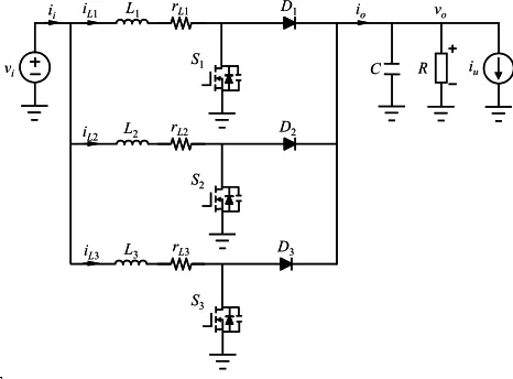
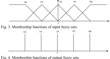
[image:3.612.52.278.334.455.2]inductor current command. In addition, the input and output fuzzy sets are both chosen as Positive Big (PB), Positive Small (PS), Zero (ZE), Negative Small (NS), and Negative Big (NB). The membership functions of input and output fuzzy sets in the voltage control loop are depicted in Figs. 3 and 4, respectively. In this study, the singleton fuzzification with triangular membership functions, center-of-gravity defuzzification, and product fuzzy inference are adopted because they are computationally simple, intuitively plausible, and most frequently used in the opening literatures [8], [9].
Fig. 3. Membership functions of input fuzzy sets.
Fig. 4. Membership functions of output fuzzy sets.
Fuzzy control is characterized by a collection of fuzzy IF-THEN rules, in which the preconditions and consequents involve linguistic variables. The rule base in the fuzzy voltage control can be represented as
l
R : If e nv( )i is 1
l
F and e nv′( )i is 2
l
F ,
Then ∆z ncd( )i is l
g (12)
where F1l and
2
l
F are input fuzzy sets; gl is the output
fuzzy set (singleton action); l=1, ," mv, where mv is the
number of rules in the voltage control loop. According to inherent circuit properties, the total inductor current command should be increased if both the voltage tracking error and its change rate are positive. On the contrary, the total inductor current command should be decreased if both the voltage tracking error and its change rate are negative. From these analyses, fuzzy linguistic rules used in the voltage control loop can be summarized in Table I. As a result, the increment of the total inductor current command produced by the fuzzy voltage control can be expressed as
1 1
/
v v
m m
cd l l l
l l
z w r w
= =
∆ =
∑
∑
(13)where rl is the singleton of the output fuzzy set, and wl
is the firing strength of the corresponding rule.
B. Current Control Loop
The input linguistic variables for the fuzzy current
control are current tracking errors e nn( )i n=1,2,3 and their
change rates e nn′( )i n=1,2,3, which are defined as
1,2,3 1,2,3 1,2,3
( ) ( ) ( )
n i n nd i n n i n
e n = ∆z n = −z n = (14)
1,2,3 1,2,3 1,2,3
( ) [ ( ) ( 1) ]/
n i n n i n n i n s
e n′ = ∆ e n = −e n − = t (15)
where z nnd( )i n=1,2,3 are respective inductor current
commands at ni-th sampling interval; z nn( )i n=1,2,3 are
respective inductor currents at ni-th sampling interval;
1,2,3
( )
n i n
e n = are respective current tracking errors at ni-th
sampling interval; e nn′( )i n=1,2,3 are the change rates of
respective current tracking errors at ni-th sampling interval.
Moreover, the output linguistic variables are respective
incremental duty ratios, ∆u nn( )i n=1,2,3. In this study, the
entire duty ratios in the fuzzy current control can be expressed as
4 1,2,3 1,2,3 (1 / )
nn nn i d
u = = ∆u = + −v z (16)
where the term (1−v zi/ 4d) represents the nominal duty
ratio of a conventional boost converter. In addition, the input and output fuzzy sets of the fuzzy current control are chosen as the same as the ones of the fuzzy voltage control. The membership functions of input and output fuzzy sets in
the current control loop are also depicted in Figs. 3and 4,
respectively. The singleton fuzzification with triangular membership functions, center-of-gravity defuzzification, and product fuzzy inference [8], [9] are also adopted here. The rule base in the fuzzy current control can be represented as
j
R : If e nn( )i n=1,2,3 is 1
j
F and e nn′( )i n=1,2,3 is 2
j
F ,
Then ∆u nn( )i n=1,2,3 is
j
g (17)
where 1
j
F and 2
j
F are input fuzzy sets; gj is the output
fuzzy set (singleton action); j=1, ," mc, where mc is the
number of rules in the current control loop.
TABLE I.
FUZZY LINGUISTIC RULES
Error Error
change rate PB PS ZE NS NB PB PB PB PB PS ZE PS PB PB PS ZE NS ZE PB PS ZE NS NB NS PS ZE NS NB NB NB ZE NS NB NB NB
According to inherent circuit properties, the duty ratio should be increased (i.e., charge the inductor more time) if both the current tracking error and its change rate are positive. On the contrary, the duty ratio should be decreased (i.e., discharge the inductor more time) if both the current tracking error and its change rate are negative. From these analyses, fuzzy linguistic rules in Table I also can be used in the current control loop. As a result, the
current control can be expressed as
1 1
/ , 1, 2, 3
c c
m m
n n n
n j j j
j j
u w r w n
= =
∆ =
∑
∑
= (18)where n
j
r is the singleton of the output fuzzy set, and n
j w
is the firing strength of the corresponding rule.
IV. NUMERICAL SIMULATIONS
In order to exhibit the merits of the proposed automatic fuzzy control (AFC) system, a conventional proportional-integral control (PIC) system is also examined in this study [6]. In this PIC scheme, the voltage tracking
error ev is obtained by subtracting z4 from z4d, and the
total amount of inductor current commands is designed as
1 1 0
t cd p v i v
z =k e +k
∫
e dt , in which kp1 and ki1 areproportional and integral gains in the voltage control loop.
Then, zcd is divided equally to z1d, z2d and z3d (i.e.,
3
t
n = ) for viewing as respective inductor current
commands, and the corresponding current tracking errors
1,2,3 1,2,3 1,2,3
nn ndn nn
e = =z = −z = are used to design the control
efforts as unn=1,2,3 =k ep2 nn=1,2,3+ −(1 v zi/ 4d), in which kp2
is a proportional gain in the current control loop. Moreover, assume that input fuzzy sets in the proposed AFC system
are symmetrical, the center ( h
r
c ) and width (wd ) of
triangular membership functions can be determined by dividing equally as
max min max
1, ,f ( 1) 1
h r h n
f
x x
c x h
n
=
−
= − −
−
" (19)
max min
2 1
d
f
x x
w
n
− =
− (20)
where nf is the total number of input/output fuzzy sets;
max
x and xmin could be predetermined maximal and
minimal bounds of ev, ev′, ∆zcd, en n=1,2,3, en n′ =1,2,3 and
1,2,3
n n
u =
∆ .
All numerical simulations are carried out using Windows packaged Matlab 6.5 edition software. The circuit specifications of a three-module boost converter
with nominal output power Po =400 W are summarized
as follows:
PWM switching frequency fs =20 kHz;
Sampling time T = µ50 s;
Inductors L1=560 Hµ ;L2=565 Hµ ;
3 584 H
L = µ ;
Output filter capacitor C=13.2 m F;
Rated output load R=5.76Ω;
Nominal input voltage vi =24V;
Nominal voltage command z4d =48V.
Moreover, the initial conditions are set at
1(0) 2(0) 3(0) 1.3889 A
z = z = z = and z4(0) = 24 V . In
addition, the control parameters of PIC and AFC systems are given as
3
t
n = , nf =5, mv =mc =25, kp1=3, ki1=5000,
2 0.045
p
k = (21)
All the parameters in (21) are chosen to achieve superior transient control performance in numerical simulations by considering the possible occurrence of operational conditions and the limitation of control efforts.
In order to investigate the robust characteristics of the proposed AFC system, the following examined cases are considered:
Case 1: Robustness against load variations. 24V
i
v = ; rL1=rL2=rL3=0; R is changed from
5.76Ω to 4.189Ω at t=0.15sec and then from
4.189Ω to 9.216Ω at t=0.30sec.
Case 2: Robustness against load variations and different equivalent series resistors of inductors.
24V
i
v = ; rL1=56mΩ ; rL2=56.5mΩ ;
3 78.4m
L
r = Ω ; R is changed from 5.76Ω to
4.189Ω at t=0.15sec and then from 4.189Ω to
9.216Ω at t=0.30sec.
Case 3: Robustness under the occurrence of
i
u.24V
i
v = ; rL1=rL2=rL3=0 ; iu =2sin(377 )t ;
5.76
R= Ω
Case 4: Robustness against load variations and different voltage commands.
24V
i
v = ; rL1=rL2=rL3=0; R is changed from
5.76Ω to 4.189Ω at t=0.15sec and then from
4.189Ω to 9.216Ω at t=0.30sec; z4d is changed
from 48V to 55V at t=0.20sec.
All the illustrations of the PIC and AFC systems are
depicted in Figs. 5−12. The sub-figure (a) is the voltage
tracking response; the sub-figure (b) is the inductor current distribution; the sub-figure (c) is the corresponding voltage tracking error; the sub-figure (d) is the corresponding current tracking errors.
(a) Time (sec) Voltage Command, z4d
Input Voltage, vi
V
Unloading (Po=250W) Loading
(Po=550W)
Output Voltage, z4
Time (sec) Voltage Tracking Error, ev
V
(b) Time (sec) Inductor Current, iL1
Inductor Current, iL2
Inductor Current, iL3
A
A
A
Time (sec)
A
Current Tracking Error, e1
Current Tracking Error, e2
Current Tracking Error, e3
A
A
(d) (a)
Time (sec) Voltage Command, z4d
Input Voltage, vi
V
Unloading (Po=250W) Loading
(Po=550W)
Output Voltage, z4
Time (sec) Voltage Tracking Error, ev
V
(b) Time (sec) Inductor Current, iL1
Inductor Current, iL2
Inductor Current, iL3
A
A
A
Time (sec)
A
Current Tracking Error, e1
Current Tracking Error, e2
Current Tracking Error, e3
A
A
[image:4.612.321.555.514.686.2](d)
Fig. 5. Numerical simulations of PIC system for three-module boost converter at case 1: (a) Voltage tracking response; (b) Inductor current distribution; (c) Voltage tracking error; (d) Current tracking error.
three-module boost converter at cases 1−4 are depicted in
Figs. 5−8, respectively. From Fig. 5(a), one can see that the
output voltage at cases 1 show a little bit dip and a slight overshoot while load variation but is eventually restored to its desired value. Basically, the average current distribution is uniform in this incremental-type PIC scheme. As can be seen from Fig. 6(a), the output voltage at case 2 also shows a slight dip while loading and a slight overshoot while unloading but rapidly restored to its desired value. At case 3, the output voltage ripple in Fig. 7(a) is distinct because the inductor current is not large enough to compensate the
effect of iu. From Fig. 8(a), the output voltage at case 4
shows a little bit dip and a slight overshoot under load variation and voltage command change. Besides, the average current distribution in Figs. 6(b) and 8(b) is not
very uniform because of the difference of rLn n=1,2,3 and
voltage commands.
(c) (a) Time (sec) Voltage Command, z4d
Input Voltage, vi
V
Unloading (Po=250W)
Loading (Po=550W)
Output Voltage, z4
Time (sec) Voltage Tracking Error, ev
V
(b) Time (sec) Inductor Current, iL1
Inductor Current, iL2
Inductor Current, iL3
A
A
A
Time (sec)
A
Current Tracking Error, e1
Current Tracking Error, e2
Current Tracking Error, e3
A A (d) (c) (a) Time (sec) Voltage Command, z4d
Input Voltage, vi
V
Unloading (Po=250W)
Loading (Po=550W)
Output Voltage, z4
Time (sec) Voltage Tracking Error, ev
V
(b) Time (sec) Inductor Current, iL1
Inductor Current, iL2
Inductor Current, iL3
A
A
A
Time (sec)
A
Current Tracking Error, e1
Current Tracking Error, e2
Current Tracking Error, e3
A
A
[image:5.612.319.559.190.364.2](d)
Fig. 6. Numerical simulations of PIC system for three-module boost converter at case 2: (a) Voltage tracking response; (b) Inductor current distribution; (c) Voltage tracking error; (d) Current tracking error.
(a) Time (sec) Voltage Command, z4d
Input Voltage, vi
V
Output Voltage, z4
Time (sec) Voltage Tracking Error, ev
V
(b) Time (sec) Inductor Current, iL1
Inductor Current, iL2
Inductor Current, iL3
A
A
A
Time (sec)
A
Current Tracking Error, e1
Current Tracking Error, e2
Current Tracking Error, e3
A
A
(c) (d)
(a) Time (sec) Voltage Command, z4d
Input Voltage, vi
V
Output Voltage, z4
Time (sec) Voltage Tracking Error, ev
V
(b) Time (sec) Inductor Current, iL1
Inductor Current, iL2
Inductor Current, iL3
A
A
A
Time (sec)
A
Current Tracking Error, e1
Current Tracking Error, e2
Current Tracking Error, e3
A
A
[image:5.612.58.292.268.440.2](c) (d)
Fig. 7. Numerical simulations of PIC system for three-module boost converter at case 3: (a) Voltage tracking response; (b) Inductor current distribution; (c) Voltage tracking error; (d) Current tracking error.
For comparison, numerical simulations of the proposed AFC system for the three-module boost converter at cases
1−4 are provided in Figs. 9−12, respectively. The control
performances at cases 1, 2 and 4 are quite stable and insensitive to the load variations or to the occurrence of different equivalent inductor series resistors and voltage commands. In other words, the output voltage rapidly stabilizes without any voltage drop or overshoot, and the average inductor current distribution is uniform. At case 3, the output voltage ripple in Fig. 7(a) can be greatly improved by the proposed AFC system, and the uniform current distribution also can be achieved. Compare Figs.
9−12 with Figs. 5−8, the proposed AFC system indeed
yields superior performance than the PIC system.
(a) Time (sec) Voltage Command, z4d
Input Voltage, vi
V
Unloading (Po=250W) Loading
(Po=550W)
Output Voltage, z4
Time (sec) Voltage Tracking Error, ev
V
(b) Time (sec) Inductor Current, iL1
Inductor Current, iL2
Inductor Current, iL3
A
A
A
Time (sec)
A
Current Tracking Error, e1
Current Tracking Error, e2
Current Tracking Error, e3
A
A
(c) (d)
(a) Time (sec) Voltage Command, z4d
Input Voltage, vi
V
Unloading (Po=250W) Loading
(Po=550W)
Output Voltage, z4
Time (sec) Voltage Tracking Error, ev
V
(b) Time (sec) Inductor Current, iL1
Inductor Current, iL2
Inductor Current, iL3
A
A
A
Time (sec)
A
Current Tracking Error, e1
Current Tracking Error, e2
Current Tracking Error, e3
A
A
[image:5.612.319.559.404.580.2](c) (d)
Fig. 8. Numerical simulations of PIC system for three-module boost converter at case 4: (a) Voltage tracking response; (b) Inductor current distribution; (c) Voltage tracking error; (d) Current tracking error.
(a) Time (sec) Voltage Command, z4d
Input Voltage, vi
V
Unloading (Po=250W) Loading
(Po=550W)
Output Voltage, z4
Time (sec) Voltage Tracking Error, ev
V
(b) Time (sec) Inductor Current, iL1
Inductor Current, iL2
Inductor Current, iL3
A
A
A
Time (sec)
A
Current Tracking Error, e1
Current Tracking Error, e2
Current Tracking Error, e3
A
A
(c) (d)
(a) Time (sec) Voltage Command, z4d
Input Voltage, vi
V
Unloading (Po=250W) Loading
(Po=550W)
Output Voltage, z4
Time (sec) Voltage Tracking Error, ev
V
(b) Time (sec) Inductor Current, iL1
Inductor Current, iL2
Inductor Current, iL3
A
A
A
Time (sec)
A
Current Tracking Error, e1
Current Tracking Error, e2
Current Tracking Error, e3
A
A
(c) (d)
Fig. 9. Numerical simulations of AFC system for three-module boost converter at case 1: (a) Voltage tracking response; (b) Inductor current distribution; (c) Voltage tracking error; (d) Current tracking error.
V. CONCLUSIONS
[image:5.612.56.295.481.655.2]According to the simulated results, one can see that the voltage regulation ability is excellent and the current sharing is very uniform even if under the possible occurrence of system uncertainties. Consequently, the proposed AFC scheme is more suitable for the parallel dc-dc converter than the traditional PIC system.
(a) Time (sec) Voltage Command, z4d
Input Voltage, vi
V
Unloading (Po=250W)
Loading (Po=550W) Output Voltage, z4
Time (sec) Voltage Tracking Error, ev
V
(b) Time (sec) Inductor Current, iL1
Inductor Current, iL2
Inductor Current, iL3
A
A
A
Time (sec)
A
Current Tracking Error, e1
Current Tracking Error, e2
Current Tracking Error, e3
A
A
(d) (a)
Time (sec) Voltage Command, z4d
Input Voltage, vi
V
Unloading (Po=250W)
Loading (Po=550W) Output Voltage, z4
Time (sec) Voltage Tracking Error, ev
V
(b) Time (sec) Inductor Current, iL1
Inductor Current, iL2
Inductor Current, iL3
A
A
A
Time (sec)
A
Current Tracking Error, e1
Current Tracking Error, e2
Current Tracking Error, e3
A
A
[image:6.612.319.559.53.229.2](d)
Fig. 10. Numerical simulations of AFC system for three-module boost converter at case 2: (a) Voltage tracking response; (b) Inductor current distribution; (c) Voltage tracking error; (d) Current tracking error.
(a) Time (sec) Voltage Command, z4d
Input Voltage, vi V Output Voltage, z4
Time (sec) Voltage Tracking Error, ev
V
(b) Time (sec) Inductor Current, iL1
Inductor Current, iL2
Inductor Current, iL3
A
A
A
Time (sec)
A
Current Tracking Error, e1
Current Tracking Error, e2
Current Tracking Error, e3
A
A
(c) (d)
Fig. 11. Numerical simulations of AFC system for three-module boost converter at case 3: (a) Voltage tracking response; (b) Inductor current distribution; (c) Voltage tracking error; (d) Current tracking error.
(a) Time (sec) Voltage Command, z4d
Input Voltage, vi
V
Unloading (Po=250W)
Loading (Po=550W)
Output Voltage, z4
Time (sec) Voltage Tracking Error, ev
V
(b) Time (sec) Inductor Current, iL1
Inductor Current, iL2
Inductor Current, iL3
A
A
A
Time (sec)
A
Current Tracking Error, e1
Current Tracking Error, e2
Current Tracking Error, e3
A
A
(c) (d)
(a) Time (sec) Voltage Command, z4d
Input Voltage, vi
V
Unloading (Po=250W)
Loading (Po=550W)
Output Voltage, z4
Time (sec) Voltage Tracking Error, ev
V
(b) Time (sec) Inductor Current, iL1
Inductor Current, iL2
Inductor Current, iL3
A
A
A
Time (sec)
A
Current Tracking Error, e1
Current Tracking Error, e2
Current Tracking Error, e3
A
A
[image:6.612.57.294.129.303.2](c) (d)
Fig. 12. Numerical simulations of AFC system for three-module boost converter at case 4: (a) Voltage tracking response; (b) Inductor current distribution; (c) Voltage tracking error; (d) Current tracking error.
REFERENCES
[1] B. Choi, “Comparative study on paralleling schemes of converter modules for distributed power applications,” IEEE Trans. Ind. Electron., vol. 45, no. 2, pp. 194-199, 1998.
[2] H. H. C. Ju and C. K. Tse, “Study of low-frequency bifurcation phenomena of a parallel-connected boost converter system via simple averaged models,” IEEE Trans. Circuits Syst. I, vol. 50, no. 5, pp. 679-686, 2003.
[3] M. López, L. G. de Vicuňa, M. Castilla, P. Gayà, and O. López, “Current distribution control design for paralleled DC/DC converters using sliding-mode control,” IEEE Trans. Ind. Electron., vol. 51, no. 2, pp. 419-428, 2004.
[4] H. Sira-Ramirez, R. A. Perez-Moreno, R. Ortega, and M. Garcia-Esteban, “Passivity-based controllers for the stabilization of DC-to-DC power converters,” Automatica, vol. 33, no. 4, pp. 499-513, 1997.
[5] G. Escobar, R. Ortega, H. Sira-Ramirez, J. P. Vilain, and I. Zein, “An experimental comparison of several nonlinear controllers for power converters,” IEEE Control System Magazine, vol. 19, no. 1, pp. 66-82, 1999.
[6] K. J. Astrom and T. Hagglund, PID Controller: Theory, Design and Tuning. Research Triangle Park, NC: ISA, 1995.
[7] S. K. Mazumder, “Stability analysis of parallel DC-DC converters,”
IEEE Trans. Aero. Electron. Syst., vol. 42, no. 1, pp. 50-69, 2006. [8] L. X. Wang, Adaptive Fuzzy Systems and Control: Design and
Stability Analysis. New Jersey: Prentice-Hall, 1994.
[9] J. R. Timothy, Fuzzy Logic with Engineering Application. New York: McGraw-Hill, 1995.
[image:6.612.57.295.342.520.2]