Boost Interleaved Converter Integrated Voltage Multiplier Module for Renewable
Energy System
1E Sandhya Rani,2Ch Vinod Kumar,3Y Srinivas Rao 1M.Tech Scholar,2Associate Professor,3Hod & Assistant Professor
Department of Electrical and Electronics Engineering, KIET-II Engineering College, Kakinada(AP), India 1[email protected];2[email protected];3[email protected]
Abstract
This document presents a high step-up converter, which is apt for renewable energy system. Through a voltage multiplier unit composed of switched capacitors and coupled inductors, a conventional interleaved boost converter obtains high step-up gain without operating at extreme duty ratio. The design of the proposed converter not only reduces the current stress but also constrains the input current ripple, which decreases the conduction losses and lengthens the lifetime of the input source. In addition, due to the lossless passive clamp performance, leakage energy is recycled to the output terminal. Hence, large voltage spikes across the main switches are alleviated, and the efficiency is improved. Even the low voltage stress makes the low-voltage-rated MOSFETs be adopted for reductions of conduction losses and cost. Finally, the prototype circuit with 40-V input voltage, 380-V output, and 1000-W output power is operated to verify its performance. The highest efficiency is 97.1%.
Index Terms - Voltage multiplier module. Boost–flyback converter, high step-up, photovoltaic (PV) system.
I. Introduction
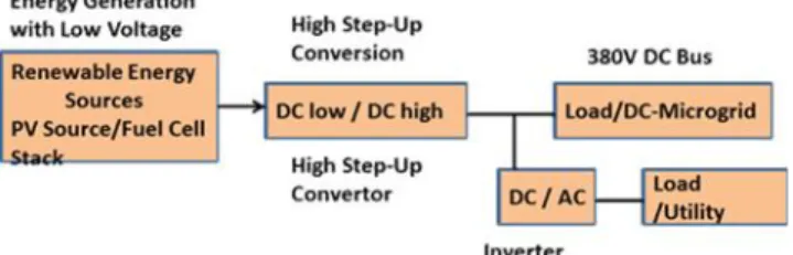
Currently renewable energy is progressively more valued and employed worldwide because of energy shortage and environmental contamination [1]–[7]. Renewable energy systems produce low voltage output, and thus, high step-up dc/dc converters have been widely employed in many renewable energy applications such fuel cells, wind power generation, and photovoltaic (PV) systems [17]–[20]. Such systems convert energy from renewable sources into electrical energy and convert low voltage into high voltage via a step-up converter, which can convert energy into electricity using a grid-by-grid inverter or dc micro grid. Fig. 1 shows a typical renewable energy system that consists of renewable energy sources, a step-up converter, and an inverter for ac application. The high step-up conversion may require two-stage converters with cascade structure for enough step-up gain, which decreases the efficiency and increases the cost. Thus, a high step-up converter is seen as an important stage in the system because such a system requires a sufficiently high step-up conversion with high efficiency.
Theoretically, conventional step-up converters, such as the boost converter and flyback converter, cannot attain a high step-up conversion with high efficiency because of the resistances of elements or leakage inductance; also, the voltage stresses are large. Thus, in recent years, many novel high step-up converters have been developed [10]–[20]. Despite these advances, high step-up single-switch converters are unsuitable to operate at heavy load given a large input current ripple, which increases conduction losses. The conventional interleaved boost converter is an excellent candidate for high-power applications and power factor correction. Unfortunately, the step-up gain is limited, and the voltage stresses on semiconductor components are equal to output voltage. Hence, based on the aforementioned considerations, modifying a conventional interleaved boost converter for high step-up and high-power application is a suitable approach. To integrate switched capacitors into an interleaved boost converter may make voltage gain reduplicate, but no service of coupled inductors causes the step-up voltage gain to be limited. Oppositely, to integrate only coupled inductors into an interleaved boost converter may make voltage gain higher and adjustable, but no employment of switched capacitors causes the step-up voltage gain to be ordinary. Thus, the synchronous employment of coupled inductors and switched capacitors is a better concept; moreover, high step-up gain, high efficiency, and low voltage stress are achieved even for high-power applications.
Fig. 1. Typical renewable energy system.
The advantages of the proposed converter are as follows. 1) The proposed converter is characterized by low input
current ripple and low conduction losses, which increases the lifetime of renewable energy sources and makes it suitable for high-power applications.
2) The converter achieves the high step-up gain that renewable energy systems require.
3) Due to the lossless passive clamp performance, leakage energy is recycled to the output terminal. Hence, large voltage spikes across the main switches are alleviated, and the efficiency is improved.
4) Low cost and high efficiency are achieved by
employment of the low-voltage-rated power switch with low RDS(ON); also, the voltage stresses on main switches
and diodes are substantially lower than output voltage. 5) The inherent configuration of the proposed converter
makes some diodes decrease conduction losses and alleviate diode reverse recovery losses.
II. Operating Principles
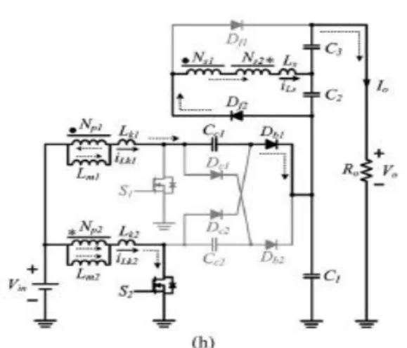
The proposed high step-up interleaved converter with a voltage multiplier module is shown in Fig. 2. The voltage multiplier module is composed of two coupled inductors and two switched capacitors and is inserted between a conventional interleaved boost converter to form a modified boost–flyback–forward interleaved structure. When the switches turn off by turn, the phase whose switch is in OFF state performs as a flyback converter, and the other phase whose switch is in ON state performs as a forward converter.
Primary windings of the coupled inductors with Np turns are employed to decrease input current ripple, and secondary windings of the coupled inductors with Ns turns are connected in series to extend voltage gain. The turn ratios of the coupled inductors are the same. The coupling references of the inductorsare denoted by “·” and “∗”.
The equivalent circuit of the proposed converter is shown in Fig. 3, where Lm1 and Lm2 are the magnetizing inductors; Lk1 and Lk2 represent the leakage inductors; Ls side; S1 and S2 denote the power switches; Cc1 and Cc2 are
the switched capacitors; and C1, C2, and C3 are the output capacitors. Dc1 and Dc2 are the clamp diodes, Db1 and Db2 represent the output diodes for boost operation with
switched capacitors, Df1 and Df2 represent the output diodes for flyback–forward operation, and n is defined as turn ratio Ns/Np.
Figure.2. Proposed High Step-up converter
Figure.3. Equivalent circuit of the proposed converter
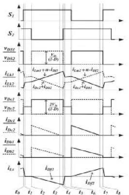
depicted in Fig. 4, and Fig. 5 shows the topological stages of the circuit.
Mode I [t0, t1]: At t = t0, the power switch S2 remains
in ON state, and the other power switch S1 begins to turn on. The diodes Dc1, Dc2, Db1, Db2, and Df1 are reversed biased, as shown in Fig. 5(a). The series leakage inductors Ls quickly release the stored energy to the output terminal via flyback–forward diode Df2, and the current through series leakage inductors Ls decreases to zero. Thus, the magnetizing inductor Lm1 still transfers energy to the secondary side of coupled inductors. The current through leakage inductor Lk1 increases linearly, and the other current through leakage inductor Lk2 decreases linearly.
Fig. 4. Steady waveform of the proposed converter in CCM.
Mode II [t1, t2]: At t = t1, both of the power switches S1
and S2 remain in ON state, and all diodes are reversed biased, as shown in Fig. 5(b). Both currents through leakage inductors Lk1 and Lk2 are increased linearly due to charging by input voltage source Vin.
Mode III [t2, t3]: At t = t2, the power switch S1 remains
in ON state, and the other power switch S2 begins to turn off. The diodes Dc1, Db1, and Df2 are reversed biased, as shown in Fig. 5(c). The energy stored in magnetizing inductor Lm2 transfers to the secondary side of coupled inductors, and the current through series leakage inductors Ls flows to output capacitor C3 via flyback–forward diodeDf1. The voltage stress on power switch S2 is
clamped by clamp capacitor Cc1 which equals the output voltage of the boost converter. The input voltage source, magnetizing inductor Lm2, leakage inductor Lk2, and clamp capacitor Cc2 release energy to the output terminal; thus, VC1 obtains a double output voltage of the boost converter.
Mode IV [t3, t4]: At t = t3, the current iDc2 has naturally
decreased to zero due to the magnetizing current distribution, and hence, diode reverse recovery losses are alleviated and conduction losses are decreased. Both power switches and all diodes remain in previous states except the clamp diode Dc2, as shown in Fig. 5(d).
Mode V [t4, t5]: At t = t4, the power switch S1 remains
in ON state, and the other power switch S2 begins to turn
on. The diodes Dc1, Dc2, Db1, Db2, and Df2 are reversed
biased, as shown in Fig. 5(e). The series leakage inductors Ls quickly release the stored energy to the output terminal via flyback–forward diode Df1, and the current through series leakage inductors decreases to zero. Thus, the magnetizing inductor Lm2 still transfers energy to the secondary side of coupled inductors. The current through leakage inductor Lk2 increases linearly, and the other current through leakage inductor Lk1 decreases linearly.
Mode VI [t5, t6]: At t = t5, both of the power switches
S1
and S2 remain in ON state, and all diodes are reversed biased, as shown in Fig. 5(f). Both currents through leakage inductors Lk1 and Lk2 are increased linearly due to
charging by input voltage source Vin.
Mode VII [t6, t7]: At t = t6, the power switch S2 remains
in ON state, and the other power switch S1 begins to turn off. The diodes Dc2, Db2, and Df1 are reversed biased, as shown in Fig. 5(g). The energy stored in magnetizing inductor Lm1 transfers to the secondary side of coupled inductors, and the current through series leakage inductors flows to output capacitor C2 via flyback–forward diode Df2. The voltage stress on power switch S1 is clamped by clamp capacitor Cc2 which equals the output voltage of the boost converter. The input voltage source, magnetizing inductor Lm1, leakage inductor Lk1, and clamp capacitor Cc1 release energy to the output terminal; thus, VC1 obtains double output voltage of the boost converter.
Mode VIII [t7, t8]: At t = t7, the current iDc1 has
Fig.5. Operating modes of the proposed converter. (a) Mode I [to, t1]. (b) Mode II [t1, t2]. (c) Mode III [t2, t3]. (d) Mode IV [t3, t4]. (e) Mode V [t4, t5]. (f) Mode VI [t5, t6]. (g) Mode VII [t6, t7]. (h) Mode VIII [t7, t8].
III. STEADY-STATE ANALYSIS
The transient characteristics of circuitry are disregarded to simplify the circuit performance analysis of the proposed converter in CCM, and some formulated assumptions are as follows.
1) All of the components in the proposed converter are ideal.
2) Leakage inductors Lk1, Lk2, and Ls are neglected. 3) Voltages on all capacitors are considered to be constant
because of infinitely large capacitance.
4) Due to the completely symmetrical interleaved structure, the related components are defined as the corresponding symbols such as Dc1 and Dc2 defined as Dc.
A. Step-Up Gain
The voltage on clamp capacitor Cc can be regarded as an output voltage of the boost converter; thus, voltage VCc can be derived from
(1)
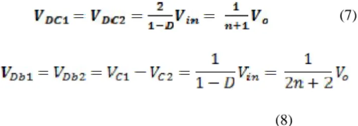
When one of the switches turns off, voltage VC1 can obtain a double output voltage of the boost converter derived from
(2)
The output filter capacitors C2 and C3 are charged by energy transformation from the primary side. When S2 is in ON state and S1 is in OFF state, VC2 is equal to the induced voltage of Ns1 plus the induced voltage of Ns2, and when S1 is in ON state and S2 is in OFF state, VC3 is also equal to the induced voltage of Ns1 plus the induced voltage of Ns2. Thus, voltages VC2 and VC3 can be derived from
(3)
The output voltage can be derived from
(4)
In addition, the voltage gain of the proposed converter is
(5)
Equation (5) confirms that the proposed converter has a high step-up voltage gain without an extreme duty cycle. The curve of the voltage gain related to turn ratio n and duty cycle is shown in Fig. 6. When the duty cycle is merely 0.6, the voltage gain reaches ten at a turn ratio n of one; the voltage gain reaches 30 at a turn ratio n of five.
Fig. 6. Voltage gain versus turn ratio n and duty cycle.
B. Voltage Stress on Semiconductor Component
The voltage ripples on the capacitors are ignored to simplify the voltage stress analysis of the components of the proposed converter.
The voltage stress on power switch S is clamped and derived from
(6)
The voltage stress on diode Dc is equal to VC1, and the voltage stress on diode Db is voltage VC1 minus voltage VCc. These voltage stresses can be derived from
(7)
(8)
The voltage stress on diode Db is close to the voltage stress on power switch S. Although the voltage stress on diode Dc is larger, it accounts for only half of output voltage Vo at a turn ratio n of one. The voltage stresses on the diodes are lower as the voltage gain is extended by increasing turn ratio n. The voltage stress on diode Df equals the VC2 plus VC3, which can be derived from
(9)
Although the voltage stress on the diode Df increases as the turn ratio n increases, the voltage stress on the diodes Df is always lower than the output voltage.
The relationship between the voltage stresses on all the semiconductor components and the turn ratio n is illustrated in Fig. 7.
Fig. 7. Voltage stresses on semiconductor components versus turn ratio n.
C. Analysis of Conduction Losses
Some conduction losses are caused by resistances of semiconductor components and coupled inductors. Thus, all the components in the proposed converter are not assumed to be ideal, except for all the capacitors. Diode reverse recovery problems, core losses, switching losses, and the equivalent series resistance of capacitors are not
discussed in this section. The characteristics of leakage inductors are disregarded because of energy recycling. The equivalent circuit, which includes the conduction losses of coupled inductors and semiconductor components, is shown in Fig. 8, in which rL1 and rL2 are the copper resistances of the primary windings of the coupled inductor; rLs represents the copper resistances of the secondary windings of the coupled inductors; rDS1 and rDS2 denote the on-resistances of power switches; VDc1, VDc2, VDb1, VDb2, VDf1, and VDf2 denote the forward biases of the diodes; and rDc1, rDc2, rDb1, rDb2, rDf1, and rDf2 are the resistances of the diodes.
Small-ripple approximation was used to calculate conduction losses. Thus, all currents that pass through components were approximated by the dc components. The magnetizing currents and capacitor voltages are assumed to be constant because of the infinite values of magnetizing inductors and capacitors. Finally, through voltage-second balance and capacitor-charge balance, the voltage conversion ratio with conduction losses can be derived from
(10) Where
Because the turn ratio n and copper resistances of the secondary windings of the coupled inductors are directly proportional, the copper resistances of the coupled inductors can be expressed as
Efficiency is expressed as follows:
(11)
than the resistances of coupled inductors and semiconductor components. In addition, the maximal effect for efficiency is duty cycle, and the secondary is the copper resistance of coupled inductors.
D. Performance of Current Distribution
The inherent configuration of the proposed converter makes the energy stored in magnetizing inductors transfer via three respective paths as one of the switches turns off. Thus, the conduction losses by lower current distribution decreases the effective value of current and increases the capacity by lower peak value of current. In addition, if the load is not heavy enough, currents through some diodes decrease to zero before they turn off, which alleviate diode reverse recovery losses.
Under light-/medium-load condition, the currents through diodes Db and Dc decrease to zero before they turn off. When the load is continuously added, only the current iDc decreases to zero before diode Dc turns off. Under heavy load, although every current through the diode cannot decrease to zero before the related diode turns off, the reduction of conduction losses and the increase of capacity still perform well
E. Consideration for Applications of Renewable Energy Source and Low-Voltage Source
Many low-voltage sources, such as battery, and renewable energy sources, such as solar cell or fuel cell stack, need a high step-up conversion to supply power to high-voltage applications and loads. However, an excellent high step-up converter not only supplies efficient step-up conversion but also should lengthen the lifetime of sources such as battery set and fuel cell stack. Thus, suppression of input current ripple for lengthening the lifetime of sources is also a main design consideration.
The proposed converter can satisfy the aforementioned applications even for high-power load due to the interleaved structure, which makes the power source or battery set discharge smoothly. The proposed converter operated in CCM is even more suitable than that operated in discontinuous conduction mode (DCM) for suppression of input current ripple, because the peak current in DCM is larger. For PV system, maximum power point tracking (MPPT) is an important consideration, and MPPT is implemented by adjusting the duty cycle within a range. However, the duty cycles of the proposed converter are greater than 0.5 due to the interleaved structure. Thus, if the proposed converter operates in some PV system, which must be satisfied with enough output voltage, duty cycle limitation, and MPPT, the turn ratio n should be set to make the maximum power point easily located in duty cycles greater than 0.5. The turn ratio n can be decreased slightly as a suitable value based on (5), which makes the duty cycle increase. Oppositely, a tradeoff should be made for practical output power to load between efficiency of the
converter and MPPT, because the larger duty cycle causes efficiency to decrease even if copper resistances decreased by smaller turn ratio n.
This section provides important information on characteristic analysis, feature, and consideration, which indicates the relationship among duty cycle, turn ratio, and components. The proposed converter for each application can be designed on the basis of selected turn ratios, components, and other considerations.
F. Performance Comparison
For demonstrating the performance of the proposed converter, the proposed converter and the other high step-up interleaved converters introduced in and are compared, as shown in Table I. The high step-up interleaved converter introduced in [36] is favorable for dc-microgrid applications, and the other high step-up interleaved converter introduced in [40] is suitable as a candidate for high step-up high-power conversion of the PV system. Both of the converters use coupled inductors and switched capacitors to achieve high step-up conversion.
Fig. 9. Measured waveforms at full load of 1000 W.
IV. Design And Experiment Of Proposed Converter
A 1-kW prototype of the proposed high step-up converter is tested. The electrical specifications are Vin = 40 V, Vo = 380 V, and fs = 40 kHz. The major components have been chosen as follows: Magnetizing inductors Lm1 and Lm2 = 133μH; turn ratio n = 1; power switches S1 and S2 are IRFP4227; diodes Dc1 and Dc2 are BYQ28E-200; diodes Db1, Db2, Df1, and Df2 are FCF06A-40; capacitors Cc1, Cc2, C2, and C3 = 220μF; and C1 = 470μF.
The design consideration of the proposed converter includes component selection and coupled inductor design, which are based on the analysis presented in the previous section. In the proposed converter, the values of the primary leakage inductors of the coupled inductors are set as close as possible for current sharing performance, and the leakage inductors Lk1 and Lk2 are 1.6
μH. Due to the performances of high step-up gain, the turn ratio n can be set as one for the prototype circuit with 40-V input voltage and 380-V output to reduce cost, volume, and conduction loss of the winding. Thus, the copper
clamped at 100 V, which is much lower than the output voltage. Fig. 9(b) shows the voltage stresses on clamp diodes and the current through clamp diodes. The voltage stresses vDc1 and vDc2 are doubles of VDS1 and VDS2. The currents iDc1 and iDc2 decrease to zero before they turn off, which alleviate diode reverse recovery losses. Fig. 9(c) shows the waveform of vDb1, vDb2, iDb1, and iDb2.
The voltage stresses vDb1 and vDb2 are equal to the voltage stresses on power switches. Fig. 9(d) shows the waveform of vDf1, vDf2, and iLs. The voltage stresses vDf1 and vDf2 are equal to vDc1 and vDc2 because the turn ratio n is set as one, and the ringing characteristics are caused by the series leakage inductors Ls. Fig. 9(e) shows the output voltage and voltages on output capacitors. The output voltage Vo is 380 V. Because the turn ratio n is set as one, the voltages VC2 and VC3 are half of VC1. From experimental results, it can be proved that the voltages on output capacitors are in accordance with those of steady-state analysis, and all of the measured voltage stresses are corresponding to those in Fig. 7, which are illustrated by theoretical analysis. Fig. 9(f) shows the input current Iin and each current through the primary leakage inductor, which demonstrates the performance of current sharing.
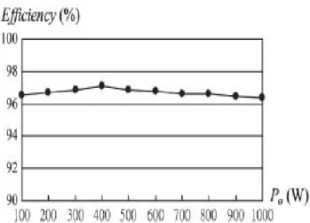
Fig. 10 shows the measured efficiency of the proposed converter. The maximum efficiency is 97.1% at Po = 400 W. At full load of 1 kW, the conversion efficiency is about 96.4%.
Fig. 10. Measured efficiency of the proposed converter.
V. Conclusion
This document has presented the theoretical analysis of steady state, related consideration, simulation results, and experimental results for the proposed converter. The proposed converter has successfully implemented an efficient high step-up conversion through the voltage multiplier module. The interleaved structure reduces the input current ripple and distributes the current through each component. In addition, the lossless passive clamp function recycles the leakage energy and constrains a large voltage
spike across the power switch. Meanwhile, the voltage stress on the power switch is restricted and much lower than the output voltage (380 V). Furthermore, the full-load efficiency is 96.4% at Po = 1000 W, and the highest efficiency is 97.1% at Po = 400 W. Thus, the proposed converter is suitable for high-power or renewable energy applications that need high step-up conversion.
VI.References
[1] Y. P. Hsieh, J. F. Chen, T. J. Liang, and L. S. Yang,
“Novel high step-up DC–DC converter for distributed
generation system,”IEEE Trans. Ind.
Electron., vol. 60, no. 4, pp. 1473–1482, Apr. 2013. [2] Y. Zhao, X. Xiang, W. Li, X. He, and C. Xia,
“Advanced symmetrical
voltage quadrupler rectifiers for high step-up and high output-voltage
converters,” IEEE Trans. Power Electron., vol. 28, no. 4, pp. 1622–1631,
Apr. 2013.
[3] Z. Song, C. Xia, and T. Liu, “Predictive current control
of three-phase
grid-connected converters with constant switching frequency for wind
energy systems,”IEEE Trans. Ind. Electron., vol. 60, no. 6, pp. 2451–
2464, Jun. 2013.
[4] Y. P. Hsieh, J. F. Chen, T. J. Liang, and L. S. Yang,
“Novel high stepup DC–DC converter with coupled-inductor and switched-capacitor techniques for a
sustainable energy system,” IEEE Trans. Power Electron., vol. 26, no. 12, pp. 3481–3490, Dec. 2011.
[5] C. T. Pan and C. M. Lai, “A high-efficiency high step-up converter with low switch voltage stress for fuel-cell
system applications,” IEEE Trans. Ind. Electron., vol. 57, no. 6, pp. 1998–2006, Jun. 2010.
[6]S. M. Chen, T. J. Liang, L. S. Yang, and J. F. Chen, “A
safety enhanced, high step-up DC–DC converter for AC
photovoltaic module application,”IEEE Trans. Power Electron., vol. 27, no. 4, pp. 1809–1817, Apr. 2012.
[7] J. T. Bialasiewicz, “Renewable energy systems with photovoltaic power generators: Operation and modeling,”
IEEE Trans. Ind. Electron., vol. 55, no. 7, pp. 2752–2758, Jul. 2008.
[8] T. Kefalas and A. Kladas, “Analysis of transformers
working under heavily saturated conditions in
grid-connected renewable energy systems,”
IEEE Trans. Ind. Electron., vol. 59, no. 5, pp. 2342–2350, May 2012.
[9] Y. Xiong, X. Cheng, Z. J. Shen, C. Mi, H. Wu, and V.
K. Garg, “Prognostic and warning system for power -electronic modules in electric, hybrid electric, and fuel-cell
vehicles,” IEEE Trans. Ind. Electron., vol. 55, no. 6, pp. 2268–2276, Jun. 2008.
[10] A. K. Rathore, A. K. S. Bhat, and R. Oruganti,
experimental results of wide range ZVS active-clamped L–
L type currentfed DC/DC converter for fuel cells to utility
interface,” IEEE Trans. Ind. Electron., vol. 59, no. 1, pp. 473–485, Jan. 2012.
[11] T. Zhou and B. Francois, “Energy management and power control of a hybrid active wind generator for distributed power generation and grid
integration,”IEEE Trans. Ind. Electron., vol. 58, no. 1, pp. 95–104, Jan.2011.
[12] N. Denniston, A. M. Massoud, S. Ahmed, and P. N.
Enjeti, “Multiplemodule high-gain high-voltage DC–DC
transformers for offshore wind energy systems,” IEEE Trans. Ind. Electron., vol. 58, no. 5, pp. 1877–1886, May 2011.
[13] H. Tao, J. L. Duarte, andM. A.M. Hendrix, “Line -interactive UPS using a fuel cell as the primary source,”
IEEE Trans. Ind. Electron., vol. 55, no. 8, pp. 3012–3021, Aug. 2008.
[14] K. Jin, X. Ruan, M. Yan, and M. Xu, “A hybrid fuel cell system,”IEEE Trans. Ind. Electron., vol. 56, no. 4, pp. 1212–1222, Apr. 2009.
[15] A. I. Bratcu, I. Munteanu, S. Bacha, D. Picault, and B.
Raison, “Cascaded DC–DC converter photovoltaic
systems: Power optimization issues,”IEEE Trans. Ind. Electron., vol. 58, no. 2, pp. 403–411, Feb. 2011.
[16] R. J. Wai, W. H. Wang, and C. Y. Lin, “High -performance stand-alone photovoltaic generation system,”
IEEE Trans. Ind. Electron., vol. 55, no. 1, pp. 240–250, Jan. 2008.
[17] Q. Zhao and F. C. Lee, “High-efficiency, high step-up DC–DC converters,” IEEE Trans. Power Electron., vol. 18, no. 1, pp. 65–73, Jan. 2003.
[18] K. C. Tseng and T. J. Liang, “Novel high-efficiency step-up converter,” Proc. Inst. Elect. Eng.—Elect. Power Appl., vol. 151, no. 2, pp. 182–190, Mar. 2004.
[19] T. J. Liang and K. C. Tseng, “Analysis of integrated
boost–flyback stepup converter,” Proc. Inst. Elect. Eng.—
Elect. Power Appl., vol. 152, no. 2, pp. 217–225, Mar. 2005.
[20] F. L. Luo, “Six self-lift DC–DC converters, voltage
lift technique,” IEEE Trans. Ind. Electron., vol. 48, no. 6, pp. 1268–1272, Dec. 2001.
Author :
E.Sandhya Rani received B.Tech degree from Kakinada Institute of Engineering & Technology for Women in 2012. Presently she is pursuing M.Tech in the Department of Electrical and Electronics Engineering in Kakinada Institute Of Engineering and Technology-II from JNTUK. Her areas of interest are Power Electronics and Drives.
Ch. Vinod Kumar received his B.Tech. degree from Jawaharlal Nehru Technological University, India, in 2005 and the M.Tech. degree from Jawaharlal Nehru Technological University-Kakinada, in 2009, both in electrical engineering, Since 2005, he has been an Assistant Professor till 2007 and HOD & Associate Professor from 2010 in the Department of Electrical and Electronics Engineering, KIET -II Engineering College. Currently working as Associate Professor in KIET -II Engineering College. His current research interests include motor drives, design and control of power electronic converters / systems, inverter-based distributed generation, hybrid electric vehicle, power systems.