International Journal of Emerging Technology and Advanced Engineering
Website: www.ijetae.com (ISSN 2250-2459, ISO 9001:2008 Certified Journal, Volume 7, Issue 9, September 2017)
551
Design and Implementation of 220V DC/DC Boost Converter
for a DC Load
Chirag Arora
1, Dr. Nagendra Kumar Swarnkar
2, Rahul Sharma
31M.Tech. Scholar, Department of Electrical Engineering, Suresh Gyan Vihar University, Jaipur, India 2Professor, Department of Electrical Engineering, Suresh Gyan Vihar University, Jaipur, India 3Assistant Professor, Department of Electrical Engineering, Suresh Gyan Vihar University, Jaipur, India Abstract: Main focus of this paper is to study and
implementation of high efficiency DC-DC circuit, based on a Boost DC/DC converter topology with high voltage gain. It is also about how to achieve high step up (efficient) DC/DC converter in the renewable power application due to low voltage of PV array. The proposed system having a solar photovoltaic module, a closed loop boost converter and a lighting module which is nothing but a DC load. Output voltage of renewable energy sources like PV modules, batteries and fuel cell is 20 V, which is boost to the range of 220V DC. If we want to connect them into grid the voltage level should be adjust like electrical network accordingly. Performance of the system is affected by the efficiency of step-up DC-DC converter. Boost converter is used to convert a low level dc input voltage coming from solar PV module to a high level dc voltage output required for the DC load.
Keyword-- High Step-Up, DC-DC Converter, Boost Converter
I. INTRODUCTION
Now a day renewable energy sources plays an important role in electricity generation. The colossal usage of fossil fuels like oil, coal and gas results in serious greenhouse effect, which has great effect on the world. People obtaining their own renewable energy system more attractive than they ever had before. The benefit of the solar PV system are relative lack of noise, implementation is easy when compared to others. As we know in India the average sunshine hour is about 6 hours and sun shine shines for about 9 months in a year [1] but this live project is made for the DC loads of Electrical Labs of the Universities and colleges which usually conducted in morning to afternoon session, so that we doesn’t use batteries and taking the power directly to the PV module at the presence of Sun. The low voltage of PV module is the biggest challenge in the case of high voltage dc application requirements. If we want to meet the high voltage requirement, many PV modules should be connected in series [3].
The characteristic of PV sources are having low DC voltage which is not suitable for the direct utilization in the grid. If we want high voltage gain from the PV module, it should be connected in series which take more physical place and number of PV modules are increased.
To get the better of this we need efficient DC/DC converter which convert low voltage gain into high voltage gain [19]. There are two types of physical converter present in market namely isolated and non-isolated based on high step-up converter. We can achieve the high voltage gain by adjusting the turn ration of the transformer because isolated converter must have a transformer i.e. fly-back, push-pull and forward type converters [15]. Similarly, if we want high voltage gain from non-isolated converter so, it is only possible by making duty cycle very large. This may cause reduced efficiency of converter because of high switching voltage stress with reverse recovery issues [8].
[image:1.595.327.532.573.755.2]Theoretically, a DC-DC boost converter provides high step-up voltage gain with extremely high duty ratio near about of 100% [9]. But the step-up voltage gain is limited due to effect of power switches and rectifier diodes practically. Many topologies have been presented to provide a high step-up voltage gain without high duty ratio [10]. The future renewable electric energy deliver and management system (FREEDM) system provides a dc interface for alternative DC sources [5].
Fig. 1 Block diagram of proposed converter.
International Journal of Emerging Technology and Advanced Engineering
Website: www.ijetae.com (ISSN 2250-2459, ISO 9001:2008 Certified Journal, Volume 7, Issue 9, September 2017)
552
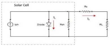
[image:2.595.333.525.139.320.2]II.CHARACTERISTIC OF SOLAR CELL AND MODULE
Fig. 3 Equivalent circuit of a solar cell.
The equivalent circuit of solar cell is shown in Fig. 2, having a internal resistance and shunt resistance of the diode. A solar module is a kind of p-n junction semiconductor which converters light energy into electrical energy. The output characteristic is expressed as[11]
[ (
( )
) ]
…… (1)
In equation (1), it is assumed that internal resistance Rs equals to zero and shunt resistance Rsh equals to infinite, thus the new equation formed as
(
) ………... (2)
Where,
K is the Boltzmann constant Q is the charge of electron
T is the operating temperature of solar cell
is the photovoltaic current
is the reverse saturation current
Operating temperature and irradiance are the major factor which affects the output voltage of solar module. Fig. 4 shows the I-V curves of the photovoltaic module. If the temperature is rising, the variation of the short circuit current is decreases. However, irradiance increasing which means the fluctuation of the open-circuit voltage is very less and the short open-circuit current has sharp fluctuation with respect to the irradiance [6].
Fig. 4 I-V curve of PV Module. (a) I-V curve influenced by different irradiances when the operating temperature is constant at 250C. (b) I-V curve influenced by the different operating temperatures when
the irradiance is constant at 0.9 kW/m2.
[image:2.595.68.262.156.238.2]Fig. 5 Actual used solar panel.
Table 1
Electrical ratings of used PV module
S. No. Electrical Values Rating
1 Maximum Power (Pmax) 100.88 W
2 Open Circuit Voltage (Voc) 22.47 V 3 Short Circuit Current (Isc) 5.57 A
4 Rated Voltage (Vmp) 18.79 V
5 Rated Current (Imp) 5.37 A
6 Module weight 9.50 KG
7 Module Dimensions 1120x675
8 Nominal Cell Temperature
(NOCT) 47±20 C
9 Maximum Temperature 850 C
[image:2.595.322.540.418.677.2]International Journal of Emerging Technology and Advanced Engineering
Website: www.ijetae.com (ISSN 2250-2459, ISO 9001:2008 Certified Journal, Volume 7, Issue 9, September 2017)
553
III. OPERATING PRINCIPLE OF PROPOSED CONVERTER
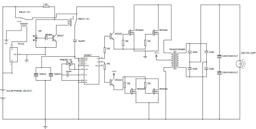
The circuit diagram of the proposed converter is shown in Fig. 6 and the experimental setup is shown in the Fig. 7, 8, 9 & 10. The converter consist of various type of component describe in the Table 2. Coming to the working the proposed converter at the very first end we have a solar panel which gives 20V DC whose positive terminal goes to IC 7812C which provides 12 V DC output to operate the relay and the ground terminal of IC goes to ground. Now 12 V supply goes to 1.3K Ω resistance and goes to relay-2 which is here to protect our circuit for overvoltage protection. The over voltage detecting element in this circuit are Zener diode and a transistor (BC547) followed by a resistance. Further the diode (1N4007) is connected to prevent the backward supply to other components. Now here is a IC called CD4047 which works in astable mode and generate the pulse in the form of pre-set value which is nothing but a variable resistance and the output is collected through the terminal 10 & 11. Here 1000µF Capacitor is used to prevent the fluctuation coming from the PV module. Further the output of the IC is goes for the base of both the transistors (IRF540N) whose collector terminal is common and emitter terminal provide the output which is amplified and the output goes to switching step-up transformer’s top and bottom terminal and middle terminal is connected to 20 V and the output terminal is goes to rectifier panel which consist of 3 ampere diodes
[image:3.595.309.524.195.425.2](5408), thus we have DC voltage which passes through 220 µF which purify the output voltage and finally the DC load which is nothing but a bulb operated at 220V.
Table 2 Required components
S. No. Component Name
Model No. / Ratings
Quantity
1 IC 7812C 1
2 12V relay 2
3 Resistance 1.3K 1
4 Resistance 10KΩ 1
5 Zener Diode 1
6 Transistor BC547 1
7 Capacitor 1000µF 2
8 Diode 1N4007 1
9 IC CD4047 1
10 Capacitor 103 µF 1
11 Resistor 100Ω 6
12 Transistor 2N2222 2
13 MOSFET 1RF540N 4
14 Transformer 12012 1
15 Diode 5408 4
16 Capacitor 220µF/450V 2
[image:3.595.81.526.476.701.2]17 Bulb 220 V, DC 1
International Journal of Emerging Technology and Advanced Engineering
Website: www.ijetae.com (ISSN 2250-2459, ISO 9001:2008 Certified Journal, Volume 7, Issue 9, September 2017)
554
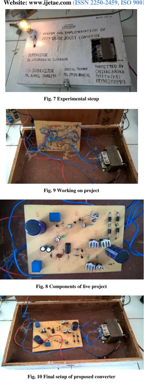
Fig. 7 Experimental steup
Fig. 9 Working on project
[image:4.595.50.280.119.740.2]Fig. 8 Components of live project
Fig. 10 Final setup of proposed converter
IV. RESULTS AND SIMULATION
In the previous view we have seen the proposed Boost converter. For the project specification which we used to make proposed converter and the components of the circuit can be calculated using the MATLAB Simulation. In this chapter we have developed a Simulink model in MATLAB Simulink environment to analyze the converter behavior to get more output from the given input which is same as of live project. Performance of the converter in Simulation environment is to be studied.
[image:4.595.314.550.387.762.2]Simulation is done on MATLAB using Simulink and results are presented. Boost converter for solar installation system is shown in the Fig. 11, input DC voltage shown in the Fig. 12, gate pulse or driving pulse is shown in the Fig. 13 which is used to drive the MOSFET. The next figure shows the voltage across the MOSFET and shown in Fig. 14, the output current is shown in the Fig. 15 which is in DC and the last but not least Fig. number 16 shows the output DC voltage. Data used in simulation studies as follows
Table 3
Study of Simulation component
S. N.
Component Values
1 Input Voltage 15 Volt
2 Output
Voltage
220-240 Volt
3 Output Current 4.77 Ampere
4 Inductance 0.1 mH
5 Capacitance 100 µF
6 Load
Resistance
50 Ω
7 Pulse
Generator
Amplitude 1
Period 10-3
Seconds
Pulse Width 70% of
period
Phase Delay 0
8 MOSFET FET
Resistance (Ron)
0.001 Ω
Internal Diode Resistance (Rd)
0.001 Ω
9 Diode Resistance
(Ron)
0.001 Ω
Forward Voltage (Vf)
0.8 V
Snubber Resistance
International Journal of Emerging Technology and Advanced Engineering
Website: www.ijetae.com (ISSN 2250-2459, ISO 9001:2008 Certified Journal, Volume 7, Issue 9, September 2017)
[image:5.595.311.546.110.599.2]555
[image:5.595.57.277.137.364.2]Fig. 11 Final setup of Boost converter
Fig. 12 Input Voltage
Fig. 13 Driving pulses of MOSFET
Fig. 14 Voltage across MOSFET
Fig. 15 Output Current
Fig. 16 Output Voltage
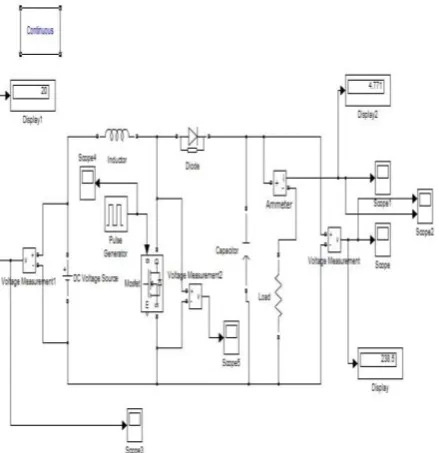
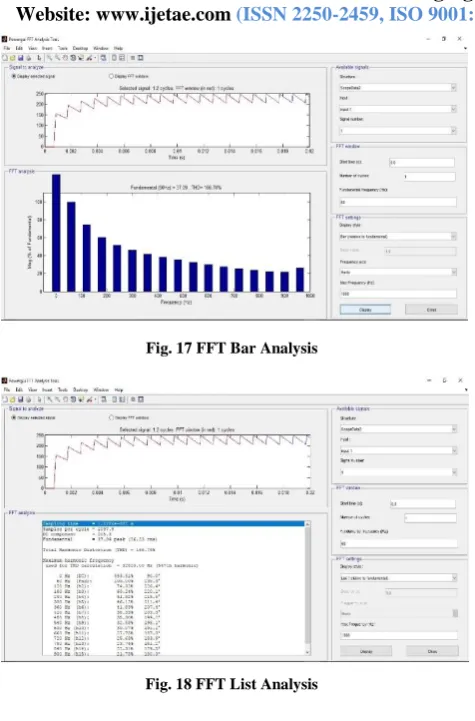
V. FFTANALYSIS
[image:5.595.52.276.390.730.2]International Journal of Emerging Technology and Advanced Engineering
Website: www.ijetae.com (ISSN 2250-2459, ISO 9001:2008 Certified Journal, Volume 7, Issue 9, September 2017)
[image:6.595.48.286.116.477.2]556
Fig. 17 FFT Bar Analysis
Fig. 18 FFT List Analysis
VI. RESULT
In the presented dissertation work, I have proposed a model and simulation of the Boost converter. For modelling the converter, I have used basic concepts of Boost converter, which we found very suitable and easy particularly for switching converters. I designed a Boost converter for a rated input voltage of 20 volt which is coming from the solar plate and output voltage 220 volt for a DC load. The derived model is simulate in MATLAB Simulink and obtained various output waveforms.
The following are the main points of my study:-
o
The labs which have DC machine should beoperated on rectifier basis and the rectifier panel needs maintenance time to time and many problems occurs in it. So, I have presented high efficiency DC-DC circuit based on DC/DC Boost converter topology with high voltage gain.
o
Design of the DC/DC Boost converter is presented in starting of the dissertation comes out very efficient and utilizable. The Simulation work of DC/DC Boost converter can be molded using Sim Library of MATLAB which, provides 220 V output to 20 V input.REFERENCES
[1] P Sathya, R Natarajan, “Design and Implementation of 12V/24V Closed loop Boost Converter for Solar Powered LED Lighting System”, International Journal of Engineering and Technology (IJET), 2013 - academia.edu
[2] A Kalirasu, SS Dash, “Simulation of Closed Loop Controlled Boost Converter for Solar Installation”, Serbian Journal of Electrical Engineering, 2010 - doiserbia.nb.rs
[3] Omar Abdel-Rahim, Mohamed Orabi, Emad Abdelkarim, Mahrous Ahmed, Mohamed Z Youssef, “Switched Inductor Boost Converter for PV Applications”, Applied Power Electronics Conference and Exposition (APEC), 2012 Twenty-Seventh Annual IEEE
[4] A Chini, F Soci, “Boost-converter-based Solar Harvester for Low Power Applications”, Electronics letters, 2010 - ieeexplore.ieee.org
[5] Zhigang Liang, Rong Guo, Jun Li, Alex Q Huang, “A High-Efficiency PV Module-Integrated DC/DC Converter for PV Energy Harvest in FREEDM System”, IEEE Transactions on Power Electronic, 2011 - ieeexplore.ieee.org
[6] Sang-Hoon Park, Gil-Ro Cha, Yong-Chae Jung, Chung-Yuen Won, “Design and application for PV generation system using a soft-switching boost converter with SARC”, IEEE Transactions on Industrial Electronics, 2010 - ieeexplore.ieee.org
[7] A Tomaszuk, A Krupa, “High Efficiency High Step-Up DC/DC Converters-a review”, Bulletin of the Polish Academy of Sciences: Technical Sciences, 2011 - degruyter.com
[8] S Saravanan, NR Babu, “Analysis and Implementation of High Step-Up DC-DC Converter for PV Based Grid Application”, Applied Energy, 2017 – Elsevier
[9] Amitava Das, Vinay Kumar Rajput, Amrita Chakraborty, Mainak Dhar, Sukanya Ray, Rakhi Dutta, “A New Transformerless DC-DC COnverter with High Voltage Gain”, Industrial Electronics, Control & Robotics (IECR), 2010International Conference, 2010 - ieeexplore.ieee.org
[10] Rong-Jong Wai, Chung-You Lin, Rou-Yong Duan, Yung-Ruei Chang, “High-Efficiency DC DC Converter with High Voltage Gain and Reduced Switch Stress”, IEEE Transactions on Industrial Electronics, 2017- ieeexplor.ieee.org
[11] ND Benavides, PL Chapman, “Modeling the effect of voltage Ripple on the Power Output of Photovoltaic Module”, IEEE Transactions on Industrial Electronics, 2008- ieeexplor.ieee.org [12] IEEE Standard for Interconnecting Distributed Resources with
Electric Power Systems, IEEE Std 1547, CD-ROM (2003). [13] J.H.R. Enslin, “The role of power electronics and storage to
increase penetration levels of renewable power”, Power and Energy Society General Meeting – Conversion and Delivery of Electrical Energy in the 21st Century, IEEE 1–2, CD-ROM (2008).
[14] S. Rehman, M.A. Ahmed, M.H. Mohamed, F.A. Al-Sulaiman, “Feasibility Study of the Grid Connected 10 MW Installed Capacity PV Power Plants in Saudi Arabia”, www.elsevier.com/ locate/ rser, 2017
[15] Furkan Dincer, “The analysis on photovoltaic electricity generation status, potential and policies of the leading countries in solar energy”, Renewable and Sustainable Energy Reviews, 2011 – Elsevier
[16] Jager-Waldau A. R&D roadmap for PV. In: Proceedings of symposium D on thin film and nano-structured materials for photovoltaics, of the E-MRS 2003 Spring Conference, March 2004, vol. 451–452; 2004. p. 448–54
International Journal of Emerging Technology and Advanced Engineering
Website: www.ijetae.com (ISSN 2250-2459, ISO 9001:2008 Certified Journal, Volume 7, Issue 9, September 2017)
557
[18] D. C. Lu, K. W. Cheng, and Y. S. Lee, “A single-switch continuous conduction- mode boost converter with reduced reverse recovery and switching losses”, IEEE Trans. Ind. Electron., vol. 50, no. 4, pp. 767 776, Aug. 2003.