DISTRIBUTION STATEMENT A: Approved for public release; distribution is unlimited.
NONRESIDENT
TRAINING
COURSE
SEPTEMBER 1998
Navy Electricity and
Electronics Training Series
Module 11—Microwave Principles
DISTRIBUTION STATEMENT A: Approved for public release; distribution is unlimited. Although the words “he,” “him,” and
i
PREFACE
By enrolling in this self-study course, you have demonstrated a desire to improve yourself and the Navy. Remember, however, this self-study course is only one part of the total Navy training program. Practical experience, schools, selected reading, and your desire to succeed are also necessary to successfully round out a fully meaningful training program.
COURSE OVERVIEW: To introduce the student to the subject of Microwave Principles who needs
such a background in accomplishing daily work and/or in preparing for further study.
THE COURSE: This self-study course is organized into subject matter areas, each containing learning
objectives to help you determine what you should learn along with text and illustrations to help you understand the information. The subject matter reflects day-to-day requirements and experiences of personnel in the rating or skill area. It also reflects guidance provided by Enlisted Community Managers (ECMs) and other senior personnel, technical references, instructions, etc., and either the occupational or naval standards, which are listed in the Manual of Navy Enlisted Manpower Personnel Classifications and Occupational Standards, NAVPERS 18068.
THE QUESTIONS: The questions that appear in this course are designed to help you understand the
material in the text.
VALUE: In completing this course, you will improve your military and professional knowledge. Importantly, it can also help you study for the Navy-wide advancement in rate examination. If you are studying and discover a reference in the text to another publication for further information, look it up.
1998 Edition Prepared by FTCM Frank E. Sloan
Published by
NAVAL EDUCATION AND TRAINING PROFESSIONAL DEVELOPMENT
AND TECHNOLOGY CENTER
ii
Sailor’s Creed
“I am a United States Sailor.
I will support and defend the
Constitution of the United States of
America and I will obey the orders
of those appointed over me.
I represent the fighting spirit of the
Navy and those who have gone
before me to defend freedom and
democracy around the world.
I proudly serve my country’s Navy
combat team with honor, courage
and commitment.
iii
TABLE OF CONTENTS
CHAPTER PAGE
1. Waveguide Theory and Application... 1-1
2. Microwave Components and Circuits ... 2-1
3. Microwave Antennas... 3-1
APPENDIX
I. Glossary... AI-1
iv
NAVY ELECTRICITY AND ELECTRONICS TRAINING
SERIES
The Navy Electricity and Electronics Training Series (NEETS) was developed for use by personnel in many electrical- and electronic-related Navy ratings. Written by, and with the advice of, senior technicians in these ratings, this series provides beginners with fundamental electrical and electronic concepts through self-study. The presentation of this series is not oriented to any specific rating structure, but is divided into modules containing related information organized into traditional paths of instruction.
The series is designed to give small amounts of information that can be easily digested before advancing further into the more complex material. For a student just becoming acquainted with electricity or electronics, it is highly recommended that the modules be studied in their suggested sequence. While there is a listing of NEETS by module title, the following brief descriptions give a quick overview of how the individual modules flow together.
Module 1, Introduction to Matter, Energy, and Direct Current, introduces the course with a short history
of electricity and electronics and proceeds into the characteristics of matter, energy, and direct current (dc). It also describes some of the general safety precautions and first-aid procedures that should be common knowledge for a person working in the field of electricity. Related safety hints are located throughout the rest of the series, as well.
Module 2, Introduction to Alternating Current and Transformers, is an introduction to alternating current
(ac) and transformers, including basic ac theory and fundamentals of electromagnetism, inductance, capacitance, impedance, and transformers.
Module 3, Introduction to Circuit Protection, Control, and Measurement, encompasses circuit breakers,
fuses, and current limiters used in circuit protection, as well as the theory and use of meters as electrical measuring devices.
Module 4, Introduction to Electrical Conductors, Wiring Techniques, and Schematic Reading, presents
conductor usage, insulation used as wire covering, splicing, termination of wiring, soldering, and reading electrical wiring diagrams.
Module 5, Introduction to Generators and Motors, is an introduction to generators and motors, and
covers the uses of ac and dc generators and motors in the conversion of electrical and mechanical energies.
Module 6, Introduction to Electronic Emission, Tubes, and Power Supplies, ties the first five modules
together in an introduction to vacuum tubes and vacuum-tube power supplies.
Module 7, Introduction to Solid-State Devices and Power Supplies, is similar to module 6, but it is in
reference to solid-state devices.
Module 8, Introduction to Amplifiers, covers amplifiers.
Module 9, Introduction to Wave-Generation and Wave-Shaping Circuits, discusses wave generation and
wave-shaping circuits.
Module 10, Introduction to Wave Propagation, Transmission Lines, and Antennas, presents the
v
Module 11, Microwave Principles, explains microwave oscillators, amplifiers, and waveguides. Module 12, Modulation Principles, discusses the principles of modulation.
Module 13, Introduction to Number Systems and Logic Circuits, presents the fundamental concepts of
number systems, Boolean algebra, and logic circuits, all of which pertain to digital computers.
Module 14, Introduction to Microelectronics, covers microelectronics technology and miniature and
microminiature circuit repair.
Module 15, Principles of Synchros, Servos, and Gyros, provides the basic principles, operations,
functions, and applications of synchro, servo, and gyro mechanisms.
Module 16, Introduction to Test Equipment, is an introduction to some of the more commonly used test
equipments and their applications.
Module 17, Radio-Frequency Communications Principles, presents the fundamentals of a
radio-frequency communications system.
Module 18, Radar Principles, covers the fundamentals of a radar system.
Module 19, The Technician's Handbook, is a handy reference of commonly used general information,
such as electrical and electronic formulas, color coding, and naval supply system data.
Module 20, Master Glossary, is the glossary of terms for the series.
Module 21, Test Methods and Practices, describes basic test methods and practices. Module 22, Introduction to Digital Computers, is an introduction to digital computers.
Module 23, Magnetic Recording, is an introduction to the use and maintenance of magnetic recorders and
the concepts of recording on magnetic tape and disks.
Module 24, Introduction to Fiber Optics, is an introduction to fiber optics.
Embedded questions are inserted throughout each module, except for modules 19 and 20, which are reference books. If you have any difficulty in answering any of the questions, restudy the applicable section.
Although an attempt has been made to use simple language, various technical words and phrases have necessarily been included. Specific terms are defined in Module 20, Master Glossary.
Considerable emphasis has been placed on illustrations to provide a maximum amount of information. In some instances, a knowledge of basic algebra may be required.
vi
Throughout the text of this course and while using technical manuals associated with the equipment you will be working on, you will find the below notations at the end of some paragraphs. The notations are used to emphasize that safety hazards exist and care must be taken or observed.
WARNING
AN OPERATING PROCEDURE, PRACTICE, OR CONDITION, ETC., WHICH MAY RESULT IN INJURY OR DEATH IF NOT CAREFULLY OBSERVED OR FOLLOWED.
CAUTION
AN OPERATING PROCEDURE, PRACTICE, OR CONDITION, ETC., WHICH MAY RESULT IN DAMAGE TO EQUIPMENT IF NOT CAREFULLY OBSERVED OR FOLLOWED.
NOTE
vii
INSTRUCTIONS FOR TAKING THE COURSE
ASSIGNMENTS
The text pages that you are to study are listed at the beginning of each assignment. Study these pages carefully before attempting to answer the questions. Pay close attention to tables and illustrations and read the learning objectives. The learning objectives state what you should be able to do after studying the material. Answering the questions correctly helps you accomplish the objectives.
SELECTING YOUR ANSWERS
Read each question carefully, then select the BEST answer. You may refer freely to the text. The answers must be the result of your own work and decisions. You are prohibited from referring to or copying the answers of others and from giving answers to anyone else taking the course.
SUBMITTING YOUR ASSIGNMENTS
To have your assignments graded, you must be enrolled in the course with the Nonresident Training Course Administration Branch at the Naval Education and Training Professional
Development and Technology Center
(NETPDTC). Following enrollment, there are two ways of having your assignments graded: (1) use the Internet to submit your assignments as you complete them, or (2) send all the assignments at one time by mail to NETPDTC.
Grading on the Internet: Advantages to
Internet grading are:
• you may submit your answers as soon as
you complete an assignment, and
• you get your results faster; usually by the next working day (approximately 24 hours).
In addition to receiving grade results for each assignment, you will receive course completion confirmation once you have completed all the
assignments. To submit your assignment
answers via the Internet, go to:
http://courses.cnet.navy.mil
Grading by Mail: When you submit answer
sheets by mail, send all of your assignments at one time. Do NOT submit individual answer sheets for grading. Mail all of your assignments in an envelope, which you either provide yourself or obtain from your nearest Educational Services Officer (ESO). Submit answer sheets to:
COMMANDING OFFICER NETPDTC N331
6490 SAUFLEY FIELD ROAD PENSACOLA FL 32559-5000
Answer Sheets: All courses include one “scannable” answer sheet for each assignment. These answer sheets are preprinted with your SSN, name, assignment number, and course number. Explanations for completing the answer sheets are on the answer sheet.
Do not use answer sheet reproductions: Use
only the original answer sheets that we
provide—reproductions will not work with our scanning equipment and cannot be processed.
Follow the instructions for marking your
answers on the answer sheet. Be sure that blocks 1, 2, and 3 are filled in correctly. This information is necessary for your course to be properly processed and for you to receive credit for your work.
COMPLETION TIME
viii
PASS/FAIL ASSIGNMENT PROCEDURES
If your overall course score is 3.2 or higher, you will pass the course and will not be required to resubmit assignments. Once your assignments have been graded you will receive course completion confirmation.
If you receive less than a 3.2 on any assignment and your overall course score is below 3.2, you will be given the opportunity to resubmit failed
assignments. You may resubmit failed
assignments only once. Internet students will
receive notification when they have failed an assignment--they may then resubmit failed assignments on the web site. Internet students
may view and print results for failed
assignments from the web site. Students who submit by mail will receive a failing result letter and a new answer sheet for resubmission of each failed assignment.
COMPLETION CONFIRMATION
After successfully completing this course, you will receive a letter of completion.
ERRATA
Errata are used to correct minor errors or delete obsolete information in a course. Errata may also be used to provide instructions to the student. If a course has an errata, it will be included as the first page(s) after the front cover. Errata for all courses can be accessed and viewed/downloaded at:
http://www.advancement.cnet.navy.mil
STUDENT FEEDBACK QUESTIONS
We value your suggestions, questions, and criticisms on our courses. If you would like to communicate with us regarding this course, we encourage you, if possible, to use e-mail. If you write or fax, please use a copy of the Student Comment form that follows this page.
For subject matter questions:
E-mail: [email protected]
Phone: Comm: (850) 452-1001, ext. 1728
DSN: 922-1001, ext. 1728 FAX: (850) 452-1370 (Do not fax answer sheets.)
Address: COMMANDING OFFICER
NETPDTC N315
6490 SAUFLEY FIELD ROAD PENSACOLA FL 32509-5237
For enrollment, shipping, grading, or completion letter questions
E-mail: [email protected]
Phone: Toll Free: 877-264-8583
Comm: (850) 452-1511/1181/1859 DSN: 922-1511/1181/1859
FAX: (850) 452-1370 (Do not fax answer sheets.)
Address: COMMANDING OFFICER
NETPDTC N331
6490 SAUFLEY FIELD ROAD PENSACOLA FL 32559-5000
NAVAL RESERVE RETIREMENT CREDIT
If you are a member of the Naval Reserve, you will receive retirement points if you are
authorized to receive them under current
directives governing retirement of Naval
Reserve personnel. For Naval Reserve
ix
Student Comments
Course Title:
NEETS Module 11
Microwave Principles
NAVEDTRA:
14183
Date:
We need some information about you:
Rate/Rank and Name: SSN: Command/Unit
Street Address: City: State/FPO: Zip
Your comments, suggestions, etc.:
Privacy Act Statement: Under authority of Title 5, USC 301, information regarding your military status is
requested in processing your comments and in preparing a reply. This information will not be divulged without written authorization to anyone other than those within DOD for official use in determining performance.
1-1
CHAPTER 1
WAVEGUIDE THEORY AND APPLICATION
LEARNING OBJECTIVES
Upon completion of this chapter the student will be able to:
1. Describe the development of the various types of waveguides in terms of their advantages and disadvantages.
2. Describe the physical dimensions of the various types of waveguides and explain the effects of those dimensions on power and frequency.
3. Explain the propagation of energy in waveguides in terms of electromagnetic field theory. 4. Identify the modes of operation in waveguides.
5. Explain the basic input/output methods used in waveguides. 6. Describe the basic principles of waveguide plumbing.
7. Explain the reasons for and the methods of terminating waveguides.
8. Explain the basic theory of operation and applications of directional couplers.
9. Describe the basic theory of operation, construction, and applications of cavity resonators. 10. Describe the basic theory of operation of waveguide junctions.
11. Explain the operation of ferrite devices in terms of their applications.
INTRODUCTION TO WAVEGUIDE THEORY AND APPLICATION
That portion of the electromagnetic spectrum which falls between 1000 megahertz and 100,000 megahertz is referred to as the MICROWAVE region. Before discussing the principles and applications of microwave frequencies, the meaning of the term microwave as it is used in this module must be established. On the surface, the definition of a microwave would appear to be simple because, in
electronics, the prefix "micro" normally means a millionth part of a unit. Micro also means small, which is a relative term, and it is used in that sense in this module. Microwave is a term loosely applied to identify electromagnetic waves above 1000 megahertz in frequency because of the short physical wavelengths of these frequencies. Short wavelength energy offers distinct advantages in many applications. For instance, excellent directivity can be obtained using relatively small antennas and low-power transmitters. These features are ideal for use in both military and civilian radar and communication applications. Small antennas and other small components are made possible by
1-2
Microwave frequencies present special problems in transmission, generation, and circuit design that are not encountered at lower frequencies. Conventional circuit theory is based on voltages and currents while microwave theory is based on electromagnetic fields. The concept of electromagnetic field
interaction is not entirely new, since electromagnetic fields form the basis of all antenna theory. However, many students of electronics find electromagnetic field theory very difficult to visualize and understand. This module will present the principles of microwave theory in the simplest terms possible but many of the concepts are still somewhat difficult to thoroughly understand. Therefore, you must realize that this module will require very careful study for you to properly understand microwave theory. Antenna fundamentals were covered in NEETS, Module 10, Introduction to Wave Propagation, Transmission Lines, and Antennas.
This module will show you the solutions to problems encountered at microwave frequencies,
beginning with the transmission of microwave energy and continuing through to waveguides in chapter 1. Later chapters will cover the theory of operation of microwave components, circuits, and antennas. The application of these concepts will be discussed more thoroughly in later NEETS modules on radar and communications.
Q-1. What is the region of the frequency spectrum from 1000 MHz to 100,000 MHz called? Q-2. Microwave theory is based upon what concept
WAVEGUIDE THEORY
The two-wire transmission line used in conventional circuits is inefficient for transferring electromagnetic energy at microwave frequencies. At these frequencies, energy escapes by radiation because the fields are not confined in all directions, as illustrated in figure 1-1. Coaxial lines are more efficient than two-wire lines for transferring electromagnetic energy because the fields are completely confined by the conductors, as illustrated in figure 1-2.
1-3
Figure 1-2.—Fields confined in all directions.
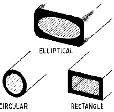
Waveguides are the most efficient way to transfer electromagnetic energy. WAVEGUIDES are essentially coaxial lines without center conductors. They are constructed from conductive material and may be rectangular, circular, or elliptical in shape, as shown in figure 1-3.
Figure 1-3.—Waveguide shapes.
Waveguide Advantages
Waveguides have several advantages over two-wire and coaxial transmission lines. For example, the large surface area of waveguides greatly reduces COPPER (I2R) LOSSES. Two-wire transmission lines
1-4
Skin effect was discussed in NEETS, Module 10, Introduction to Wave Propagation, Transmission Lines, and Antennas, Chapter 3. Skin effect tends to increase the effective resistance of the conductor. Although energy transfer in coaxial cable is caused by electromagnetic field motion, the magnitude of the field is limited by the size of the current-carrying area of the inner conductor. The small size of the center conductor is even further reduced by skin effect and energy transmission by coaxial cable becomes less efficient than by waveguides. DIELECTRIC LOSSES are also lower in waveguides than in two-wire and coaxial transmission lines. Dielectric losses in two-wire and coaxial lines are caused by the heating of the insulation between the conductors. The insulation behaves as the dielectric of a capacitor formed by the two wires of the transmission line. A voltage potential across the two wires causes heating of the dielectric and results in a power loss. In practical applications, the actual breakdown of the insulation between the conductors of a transmission line is more frequently a problem than is the dielectric loss.
This breakdown is usually caused by stationary voltage spikes or "nodes" which are caused by standing waves. Standing waves are stationary and occur when part of the energy traveling down the line is reflected by an impedance mismatch with the load. The voltage potential of the standing waves at the points of greatest magnitude can become large enough to break down the insulation between transmission line conductors.
The dielectric in waveguides is air, which has a much lower dielectric loss than conventional insulating materials. However, waveguides are also subject to dielectric breakdown caused by standing waves. Standing waves in waveguides cause arcing which decreases the efficiency of energy transfer and can severely damage the waveguide. Also since the electromagnetic fields are completely contained within the waveguide, radiation losses are kept very low.
Power-handling capability is another advantage of waveguides. Waveguides can handle more power than coaxial lines of the same size because power-handling capability is directly related to the distance between conductors. Figure 1-4 illustrates the greater distance between conductors in a waveguide.
Figure 1-4.—Comparison of spacing in coaxial cable and a circular waveguide.
1-5
Waveguide Disadvantages
Physical size is the primary lower-frequency limitation of waveguides. The width of a waveguide must be approximately a half wavelength at the frequency of the wave to be transported. For example, a waveguide for use at 1 megahertz would be about 500 feet wide. This makes the use of waveguides at frequencies below 1000 megahertz increasingly impractical. The lower frequency range of any system using waveguides is limited by the physical dimensions of the waveguides.
Waveguides are difficult to install because of their rigid, hollow-pipe shape. Special couplings at the joints are required to assure proper operation. Also, the inside surfaces of waveguides are often plated with silver or gold to reduce skin effect losses. These requirements increase the costs and decrease the practicality of waveguide systems at any other than microwave frequencies.
Q-3. Why are coaxial lines more efficient at microwave frequencies than two-wire transmission lines? Q-4. What kind of material must be used in the construction of waveguides?
Q-5. The large surface area of a waveguide greatly reduces what type of loss that is common in two-wire and coaxial lines?
Q-6. What causes the current-carrying area at the center conductor of a coaxial line to be restricted to a small layer at the surface?
Q-7. What is used as a dielectric in waveguides?
Q-8. What is the primary lower-frequency limitation of waveguides?
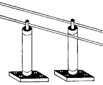
Developing the Waveguide from Parallel Lines
You may better understand the transition from ordinary transmission line concepts to waveguide theories by considering the development of a waveguide from a two-wire transmission line. Figure 1-5 shows a section of two-wire transmission line supported on two insulators. At the junction with the line, the insulators must present a very high impedance to ground for proper operation of the line. A low impedance insulator would obviously short-circuit the line to ground, and this is what happens at very high frequencies. Ordinary insulators display the characteristics of the dielectric of a capacitor formed by the wire and ground. As the frequency increases, the overall impedance decreases. A better
high-frequency insulator is a quarter-wave section of transmission line shorted at one end. Such an insulator is shown in figure 1-6. The impedance of a shorted quarter-wave section is very high at the open-end junction with the two-wire transmission line. This type of insulator is known as a METALLIC
1-6
Figure 1-5.—Two-wire transmission line using ordinary insulators.
Figure 1-6.—Quarter-wave section of transmission line shorted at one end.
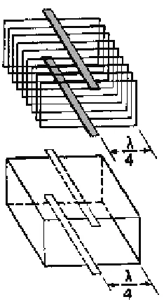
[image:18.612.217.397.73.223.2]Figure 1-7 shows several metallic insulators on each side of a two-wire transmission line. As more insulators are added, each section makes contact with the next, and a rectangular waveguide is formed. The lines become part of the walls of the waveguide, as illustrated in figure 1-8. The energy is then conducted within the hollow waveguide instead of along the two-wire transmission line.
1-7
Figure 1-8.—Forming a waveguide by adding quarter-wave sections.
The comparison of the way electromagnetic fields work on a transmission line and in a waveguide is not exact. During the change from a two-wire line to a waveguide, the electromagnetic field
configurations also undergo many changes. These will be discussed later in this chapter. As a result of these changes, the waveguide does not actually operate like a two-wire line that is completely shunted by quarter-wave sections. If it did, the use of a waveguide would be limited to a single-frequency wavelength that was four times the length of the quarter-wave sections. In fact, waves of this length cannot pass efficiently through waveguides. Only a small range of frequencies of somewhat shorter wavelength (higher frequency) can pass efficiently.
[image:19.612.245.362.72.289.2]As shown in figure 1-9, the widest dimension of a waveguide is called the "a" dimension and determines the range of operating frequencies. The narrowest dimension determines the power-handling capability of the waveguide and is called the "b" dimension.
1-8
NOTE
This method of labeling waveguides is not standard in all texts. Different methods may be used in other texts on microwave principles, but this method is in accordance with Navy Military Standards (MIL-STDS).
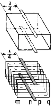
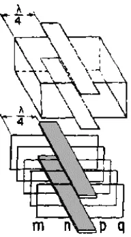
The ability of a waveguide of a given dimension to transport more than one frequency may be better understood by analyzing the actions illustrated in figure 1-10A, B, and C. A waveguide may be
[image:20.612.254.340.247.419.2]considered as having upper and lower quarter-wave sections and a central section which is a solid conductor called a BUS BAR. In figure 1-10A, distance mn is equal to distance pq, and both are equal to one quarter-wavelength (!/4).
Figure 1-10A.—Frequency effects on a waveguide. NORMAL OPERATING FREQUENCY.
NOTE
Throughout NEETS, 1/4! and !/4 are both used to represent one quarter-wavelength and are used interchangeably. Also, !/2 and 3/2! will be used to represent one half-wavelength and 1 1/2 wavelengths, respectively.
1-9
[image:21.612.249.345.73.246.2]Figure 1-10B.—Frequency effects on a waveguide. INCREASING FREQUENCY.
Figure 1-10C.—Frequency effects on a waveguide. DECREASING FREQUENCY.
If the frequency of a signal is decreased so much that two quarter-wavelengths are longer than the wide dimension of a waveguide, energy will no longer pass through the waveguide. This is the lower frequency limit, or CUT-OFF FREQUENCY, of a given waveguide. In practical applications, the wide dimension of a waveguide is usually 0.7 wavelength at the operating frequency. This allows the
waveguide to handle a small range of frequencies both above and below the operating frequency. The "b" dimension is governed by the breakdown potential of the dielectric, which is usually air. Dimensions ranging from 0.2 to 0.5 wavelength are common for the "b" sides of a waveguide.
1-10
Q-11. The frequency range of a waveguide is determined by what dimensison?
Q-12. What happens to the bus bar dimensions of the waveguide when the frequency is increased? Q-13. When the frequency is decreased so that two quarter-wavelengths are longer than the "a" (wide)
dimension of the waveguide, what will happen?
Energy Propagation in Waveguides
Since energy is transferred through waveguides by electromagnetic fields, you need a basic understanding of field theory. Both magnetic (H FIELD) and electric field (E FIELD) are present in waveguides, and the interaction of these fields causes energy to travel through the waveguide. This action is best understood by first looking at the properties of the two individual fields.
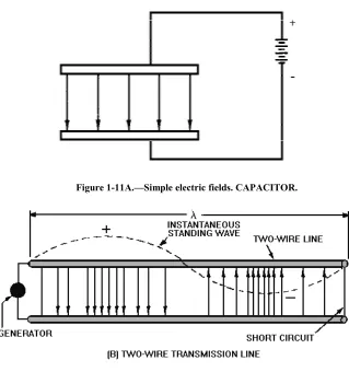
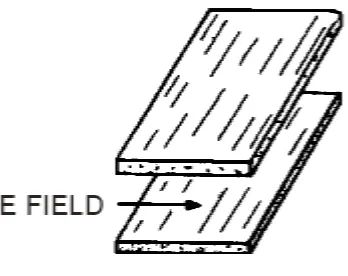
E FIELD.An electric field exists when a difference of potential causes a stress in the dielectric between two points. The simplest electric field is one that forms between the plates of a capacitor when one plate is made positive compared to the other, as shown in figure 1-11A. The stress created in the dielectric is an electric field.
Electric fields are represented by arrows that point from the positive toward the negative potential. The number of arrows shows the relative strength of the field. In figure 1-11A, for example, evenly spaced arrows indicate the field is evenly distributed. For ease of explanation, the electric field is abbreviated E field, and the lines of stress are called E lines.
[image:22.612.146.465.351.691.2]Figure 1-11A.—Simple electric fields. CAPACITOR.
1-11
The two-wire transmission line, illustrated in figure 1-11B, has an instantaneous standing wave of voltage applied to it by the generator. The line is short-circuited at one-wavelength, at the positive and negative voltage peaks, but the arrows, representing each field, point in opposite directions. The voltage across the line varies sinusoidally. Therefore, the density of the E-lines varies sinusoidally.
The development of the E field in a waveguide can be illustrated by a two-wire transmission line separated by several, double quarter-wave sections, called half-wave frames, as illustrated in figure 1-12. As shown, the voltage across the two-wire line varies in a sine-wave pattern and the density of the E field also varies in a sine-wave pattern. The half-wave frames located at high-voltage points (1) and (3) have a strong E field. The frames at the zero-voltage points (2) have no E fields present. Frame (4) has a weak E field and is located at a point between maximum and minimum voltage. This illustration is a buildup to the three-dimensional aspect of the full E field in a waveguide.
Figure 1-12.—E fields on a two-wire line with half-wave frames.
Figure 1-13, view (A), shows the E-field pattern created by a voltage sine wave applied to a
1-12
Figure 1-13.—E field of a voltage standing wave across a 1-wavelength section of a waveguide.
H FIELD.The magnetic field in a waveguide is made up of magnetic lines of force that are caused by current flow through the conductive material of the waveguide. Magnetic lines of force, called H lines, are continuous closed loops, as shown in figure 1-14. All of the H lines associated with current are collectively called a magnetic field or H field. The strength of the H field, indicated by the number of H lines in a given area, varies directly with the amount of current.
Figure 1-14.—Magnetic field on a single wire.
1-13
Figure 1-15.—Magnetic field on a coil.
A similar action takes place in a waveguide. In figure 1-16A, a two-wire line with quarter-wave sections is shown. Currents flow in the main line and in the quarter-wave sections. The current direction produces the individual H lines around each conductor as shown. When a large number of sections exist, the fields cancel between the sections, but the directions are the same both inside and outside the
waveguide. At half-wave intervals on the main line, current will flow in opposite directions. This
produces H-line loops having opposite directions. In figure 1-16A, current at the left end is opposite to the current at the right end. The individual loops on the main line are opposite in direction. All around the framework they join so that the long loop shown in figure 1-16B is formed. Outside the waveguide the individual loops cannot join to form a continuous loop. Thus, no magnetic field exists outside a waveguide.
1-14
Figure 1-16B.—Magnetic fields on a two-wire line with half-wave frames.
If the two-wire line and the half-wave frames are developed into a waveguide that is closed at both ends (as shown in figure 1-16B), the distribution of H lines will be as shown in figure 1-17. If the waveguide is extended to 1 1/2!, these H lines form complete loops at half-wave intervals with each group reversed in direction. Again, no H lines can form outside the waveguide as long as it is completely enclosed.
Figure 1-17.—Magnetic field pattern in a waveguide.
Figure 1-18 shows a cross-sectional view of the magnetic field pattern illustrated in figure 1-17. Note in view (A) that the field is strongest at the edges of the waveguide where the current is highest. The minimum field strength occurs at the zero-current points. View (B) shows the field pattern as it appears
1-15
Figure 1-18.—Magnetic field in a waveguide three half-wavelengths long.
BOUNDARY CONDITIONS IN A WAVEGUIDE.The travel of energy down a waveguide is
similar, but not identical, to the travel of electromagnetic waves in free space. The difference is that the energy in a waveguide is confined to the physical limits of the guide. Two conditions, known as BOUNDARY CONDITIONS, must be satisfied for energy to travel through a waveguide.
The first boundary condition (illustrated in figure 1-19A) can be stated as follows:
For an electric field to exist at the surface of a conductor it must be perpendicular to the conductor.
Figure 1-19A.—E field boundary condition. MEETS BOUNDARY CONDITIONS.
1-16
Figure 1-19B.—E field boundary condition. DOES NOT MEET BOUNDARY CONDITIONS.
The second boundary condition, which is illustrated in figure 1-20, can be stated as follows:
For a varying magnetic field to exist, it must form closed loops in parallel with the conductors and be perpendicular to the electric field.
Figure 1-20.—H field boundary condition.
Since an E field causes a current flow that in turn produces an H field, both fields always exist at the same time in a waveguide. If a system satisfies one of these boundary conditions, it must also satisfy the other since neither field can exist alone. You should briefly review the principles of electromagnetic propagation in free space (NEETS, Module 10, Introduction to Wave Propagation, Transmission Lines, and Antennas). This review will help you understand how a waveguide satisfies the two boundary conditions necessary for energy propagation in a waveguide.
WAVEFRONTS WITHIN A WAVEGUIDE.Electromagnetic energy transmitted into space
[image:28.612.217.407.352.487.2]1-17
Figure 1-21.—The Poynting vector.
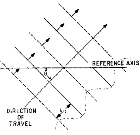
The combined electric and magnetic fields form a wavefront that can be represented by alternate negative and positive peaks at half-wavelength intervals, as illustrated in figure 1-22. Angle " is the direction of travel of the wave with respect to some reference axis.
Figure 1-22.—Wavefronts in space.
1-18
Figure 1-23.—Combined wavefronts.
If two conductive plates are placed along cancellation lines D and E or cancellation lines B and G, the first boundary condition for waveguides will be satisfied; that is, the E fields will be zero at the surface of the conductive plates. The second boundary condition is, therefore, automatically satisfied. Since these plates serve the same purpose as the "b" dimension walls of a waveguide, the "a" dimension walls can be added without affecting the magnetic or electric fields.
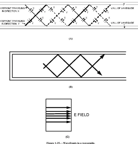
When a quarter-wavelength probe is inserted into a waveguide and supplied with microwave energy, it will act as a quarter-wave vertical antenna. Positive and negative wavefronts will be radiated, as shown in figure 1-24. Any portion of the wavefront traveling in the direction of arrow C will rapidly decrease to zero because it does not fulfill either of the required boundary conditions. The parts of the wavefronts that travel in the directions of arrows A and B will reflect from the walls and form reverse-phase wavefronts. These two wavefronts, and those that follow, are illustrated in figure 1-25. Notice that the wavefronts crisscross down the center of the waveguide and produce the same resultant field pattern that was shown in figure 1-23.
1-19
(A)
(B)
[image:31.612.81.541.70.548.2](C)
Figure 1-25.—Wavefronts in a waveguide.
The reflection of a single wavefront off the "b" wall of a waveguide is shown in figure 1-26. The wavefront is shown in view (A) as small particles. In views (B) and (C) particle 1 strikes the wall and is bounced back from the wall without losing velocity. If the wall is perfectly flat, the angle at which it strikes the wall, known as the angle of incidence ("), is the same as the angle of reflection (ø) and are measured perpendicular to the waveguide surface. An instant after particle 1 strikes the wall, particle 2 strikes the wall, as shown in view (C), and reflects in the same manner. Because all the particles are traveling at the same velocity, particles 1 and 2 do not change their relative position with respect to each other. Therefore, the reflected wave has the same shape as the original. The remaining particles as shown in views (D), (E) and (F) reflect in the same manner. This process results in a reflected wavefront
1-20
Figure 1-26.—Reflection of a single wavefront.
Figures 1-27A and 1-27B, each illustrate the direction of propagation of two different
1-21
Figure 1-27A.—Different frequencies in a waveguide.
Figure 1-27B.—Different frequencies in a waveguide.
The velocity of propagation of a wave along a waveguide is less than its velocity through free space (speed of light). This lower velocity is caused by the zigzag path taken by the wavefront. The
forward-progress velocity of the wavefront in a waveguide is called GROUP VELOCITY and is somewhat slower than the speed of light.
[image:33.612.242.373.336.548.2]1-22
Figure 1-28A.—Reflection angle at various frequencies. LOW FREQUENCY.
Figure 1-28B.—Reflection angle at various frequencies. MEDIUM FREQUENCY.
Figure 1-28C.—Reflection angle at various frequencies. HIGH FREQUENCY.
Q-14. What interaction causes energy to travel down a waveguide?
Q-15. What is indicated by the number of arrows (closeness of spacing) used to represent an electric field?
Q-16. What primary condition must magnetic lines of force meet in order to exist?
Q-17. What happens to the H lines between the conductors of a coil when the conductors are close together?
Q-18. For an electric field to exist at the surface of a conductor, the field must have what angular relationship to the conductor?
Q-19. When a wavefront is radiated into a waveguide, what happens to the portions of the wavefront that do not satisfy the boundary conditions?
Q-20. Assuming the wall of a waveguide is perfectly flat, what is the angular relationship between the angle of incidence and the angle of reflection?
Q-21. What is the frequency called that produces angles of incidence and reflection that are perpendicular to the waveguide walls?
1-23
Q-23. What term is used to identify the forward progress velocity of wavefronts in a waveguide?
Waveguide Modes of Operation
The waveguide analyzed in the previous paragraphs yields an electric field configuration known as the half-sine electric distribution. This configuration, called a MODE OF OPERATION, is shown in figure 1-29. Recall that the strength of the field is indicated by the spacing of the lines; that is, the closer the lines, the stronger the field. The regions of maximum voltage in this field move continuously down the waveguide in a sine-wave pattern. To meet boundary conditions, the field must always be zero at the "b" walls.
The half-sine field is only one of many field configurations, or modes, that can exist in a rectangular waveguide. A full-sine field can also exist in a rectangular waveguide because, as shown in figure 1-30, the field is zero at the "b" walls.
Similarly, a 1 1/2 sine-wave field can exist in a rectangular waveguide because this field also meets the boundary conditions. As shown in figure 1-31, the field is perpendicular to any conducting surface it touches and is zero along the "b" walls.
Figure 1-29.—Half-sine E field distribution.
1-24
Figure 1-31.—One and one-half sine E field distribution.
The magnetic field in a rectangular waveguide is in the form of closed loops parallel to the surface of the conductors. The strength of the magnetic field is proportional to the electric field. Figure 1-32
illustrates the magnetic field pattern associated with a half-sine electric field distribution. The magnitude of the magnetic field varies in a sine-wave pattern down the center of the waveguide in "time phase" with the electric field. TIME PHASE means that the peak H lines and peak E lines occur at the same instant in time, although not necessarily at the same point along the length of the waveguide.
Figure 1-32.—Magnetic field caused by a half-sine E field.
An electric field in a sine-wave pattern also exists down the center of a waveguide. In figure 1-33, view (A), consider the two wavefronts, C and D. Assume that they are positive at point 1 and negative at point 2. When the wavefronts cross at points 1 and 2, each field is at its maximum strength. At these points, the fields combine, further increasing their strength. This action is continuous because each wave is always followed by a replacement wave. Figure 1-33, view (B), illustrates the resultant sine
configuration of the electric field at the center of the waveguide. This configuration is only one of the many field patterns that can exist in a waveguide. Each configuration forms a separate mode of operation. The easiest mode to produce is called the DOMINANT MODE. Other modes with different field
1-25
Figure 1-33.—Crisscrossing wavefronts and the resultant E field.
The dominant mode is the most efficient mode. Waveguides are normally designed so that only the dominant mode will be used. To operate in the dominant mode, a waveguide must have an "a" (wide) dimension of at least one half-wavelength of the frequency to be propagated. The "a" dimension of the waveguide must be kept near the minimum allowable value to ensure that only the dominant mode will exist. In practice, this dimension is usually 0.7 wavelength.
Of the possible modes of operation available for a given waveguide, the dominant mode has the lowest cutoff frequency. The high-frequency limit of a rectangular waveguide is a frequency at which its "a" dimension becomes large enough to allow operation in a mode higher than that for which the
waveguide has been designed.
Waveguides may be designed to operate in a mode other than the dominant mode. An example of a full-sine configuration mode is shown in figures 1-34A and 1-34B. The "a" dimension of the waveguide in this figure is one wavelength long. You may assume that the two-wire line is 1/4! from one of the "b" walls, as shown in figure 1-34A. The remaining distance to the other "b" wall is 3/4!. The three-quarter wavelength section has the same high impedance as the quarter-wave section; therefore, the two-wire line is properly insulated. The field configuration shows a complete sine-wave pattern across the "a"
dimension, as illustrated in figure 1-34B.
[image:37.612.225.382.522.680.2]1-26
Figure 1-34B.—Waveguide operation in other than dominant mode.
Circular waveguides are used in specific areas of radar and communications systems, such as
rotating joints used at the mechanical point where the antennas rotate. Figure 1-35 illustrates the dominant mode of a circular waveguide. The cutoff wavelength of a circular guide is 1.71 times the diameter of the waveguide. Since the "a" dimension of a rectangular waveguide is approximately one half-wavelength at the cutoff frequency, the diameter of an equivalent circular waveguide must be 2 ÷ 1.71, or approximately 1.17 times the "a" dimension of a rectangular waveguide.
Figure 1-35.—Dominant mode in a circular waveguide.
MODE NUMBERING SYSTEMS.So far, only the most basic types of E and H field
arrangements have been shown. More complicated arrangements are often necessary to make possible coupling, isolation, or other types of operation. The field arrangements of the various modes of operation are divided into two categories: TRANSVERSE ELECTRIC (TE) and TRANSVERSE MAGNETIC (TM).
[image:38.612.185.413.355.556.2]1-27
In the transverse magnetic (TM) mode, the entire magnetic field is in the transverse plane and has no portion parallel to the length axis.
Since there are several TE and TM modes, subscripts are used to complete the description of the field pattern. In rectangular waveguides, the first subscript indicates the number of half-wave patterns in the "a" dimension, and the second subscript indicates the number of half-wave patterns in the "b" dimension.
The dominant mode for rectangular waveguides is shown in figure 1-36. It is designated as the TE mode because the E fields are perpendicular to the "a" walls. The first subscript is 1 since there is only one half-wave pattern across the "a" dimension. There are no E-field patterns across the "b" dimension, so the second subscript is 0. The complete mode description of the dominant mode in rectangular
waveguides is TE1,0. Subsequent descriptions of waveguide operation in this text will assume the
dominant (TE1,0) mode unless otherwise noted.
Figure 1-36.—Dominant mode in a rectangular waveguide.
A similar system is used to identify the modes of circular waveguides. The general classification of TE and TM is true for both circular and rectangular waveguides. In circular waveguides the subscripts have a different meaning. The first subscript indicates the number of full-wave patterns around the circumference of the waveguide. The second subscript indicates the number of half-wave patterns across the diameter.
In the circular waveguide in figure 1-37, the E field is perpendicular to the length of the waveguide with no E lines parallel to the direction of propagation. Thus, it must be classified as operating in the TE mode. If you follow the E line pattern in a counterclockwise direction starting at the top, the E lines go from zero, through maximum positive (tail of arrows), back to zero, through maximum negative (head of arrows), and then back to zero again. This is one full wave, so the first subscript is 1. Along the diameter, the E lines go from zero through maximum and back to zero, making a half-wave variation. The second subscript, therefore, is also 1. TE 1,1 is the complete mode description of the dominant mode in circular
1-28
Figure 1-37.—Counting wavelengths in a circular waveguide.
Figure 1-38.—Various modes of operation for rectangular and circular waveguides.
Waveguide Input/Output Methods
A waveguide, as explained earlier in this chapter, operates differently from an ordinary transmission line. Therefore, special devices must be used to put energy into a waveguide at one end and remove it from the other end.
[image:40.612.56.562.310.554.2]1-29
As previously discussed, when a small probe is inserted into a waveguide and supplied with microwave energy, it acts as a quarter-wave antenna. Current flows in the probe and sets up an E field such as the one shown in figure 1-39A. The E lines detach themselves from the probe. When the probe is located at the point of highest efficiency, the E lines set up an E field of considerable intensity.
Figure 1-39A.—Probe coupling in a rectangular waveguide.
[image:41.612.237.377.158.297.2]Figure 1-39B.—Probe coupling in a rectangular waveguide.
1-30
Figure 1-39D.—Probe coupling in a rectangular waveguide.
The most efficient place to locate the probe is in the center of the "a" wall, parallel to the "b" wall, and one quarter-wavelength from the shorted end of the waveguide, as shown in figure 1-39B, and figure 1-39C. This is the point at which the E field is maximum in the dominant mode. Therefore, energy transfer (coupling) is maximum at this point. Note that the quarter-wavelength spacing is at the frequency required to propagate the dominant mode.
In many applications a lesser degree of energy transfer, called loose coupling, is desirable. The amount of energy transfer can be reduced by decreasing the length of the probe, by moving it out of the center of the E field, or by shielding it. Where the degree of coupling must be varied frequently, the probe is made retractable so the length can be easily changed.
The size and shape of the probe determines its frequency, bandwidth, and power-handling capability. As the diameter of a probe increases, the bandwidth increases. A probe similar in shape to a door knob is capable of handling much higher power and a larger bandwidth than a conventional probe. The greater power-handling capability is directly related to the increased surface area. Two examples of
broad-bandwidth probes are illustrated in figure 1-39D. Removal of energy from a waveguide is simply a reversal of the injection process using the same type of probe.
Another way of injecting energy into a waveguide is by setting up an H field in the waveguide. This can be accomplished by inserting a small loop which carries a high current into the waveguide, as shown in figure 1-40A. A magnetic field builds up around the loop and expands to fit the waveguide, as shown in figure 1-40B. If the frequency of the current in the loop is within the bandwidth of the waveguide, energy will be transferred to the waveguide.
1-31
Figure 1-40A.—Loop coupling in a rectangular waveguide.
Figure 1-40B.—Loop coupling in a rectangular waveguide.
Figure 1-40C.—Loop coupling in a rectangular waveguide.
When less efficient coupling is desired, you can rotate or move the loop until it encircles a smaller number of H lines. When the diameter of the loop is increased, its power-handling capability also increases. The bandwidth can be increased by increasing the size of the wire used to make the loop.
1-32
Slots or apertures are sometimes used when very loose (inefficient) coupling is desired, as shown in figure 1-41. In this method energy enters through a small slot in the waveguide and the E field expands into the waveguide. The E lines expand first across the slot and then across the interior of the waveguide.
Minimum reflections occur when energy is injected or removed if the size of the slot is properly proportioned to the frequency of the energy.
Figure 1-41.—Slot coupling in a waveguide.
After learning how energy is coupled into and out of a waveguide with slots, you might think that leaving the end open is the most simple way of injecting or removing energy in a waveguide. This is not the case, however, because when energy leaves a waveguide, fields form around the end of the
waveguide. These fields cause an impedance mismatch which, in turn, causes the development of standing waves and a drastic loss in efficiency. Various methods of impedance matching and terminating waveguides will be covered in the next section.
Q-24. What term is used to identify each of the many field configurations that can exist in waveguides? Q-25. What field configuration is easiest to produce in a given waveguide?
Q-26. How is the cutoff wavelength of a circular waveguide figured?
Q-27. The field arrangements in waveguides are divided into what two categories to describe the various modes of operation?
Q-28. The electric field is perpendicular to the "a" dimension of a waveguide in what mode?
Q-29. The number of half-wave patterns in the "b" dimension of rectangular waveguides is indicated by which of the two descriptive subscripts?
Q-30. Which subscript, in circular waveguide classification, indicates the number of full-wave patterns around the circumference?
1-33
Q-32. Loose or inefficient coupling of energy into or out of a waveguide can be accomplished by the use of what method?
Waveguide Impedance Matching
Waveguide transmission systems are not always perfectly impedance matched to their load devices. The standing waves that result from a mismatch cause a power loss, a reduction in power-handling capability, and an increase in frequency sensitivity. Impedance-changing devices are therefore placed in the waveguide to match the waveguide to the load. These devices are placed near the source of the standing waves.
Figure 1-42 illustrates three devices, called irises, that are used to introduce inductance or
capacitance into a waveguide. An iris is nothing more than a metal plate that contains an opening through which the waves may pass. The iris is located in the transverse plane.
Figure 1-42.—Waveguide irises.
An inductive iris and its equivalent circuit are illustrated in figure 1-42, view (A). The iris places a shunt inductive reactance across the waveguide that is directly proportional to the size of the opening. Notice that the edges of the inductive iris are perpendicular to the magnetic plane. The shunt capacitive reactance, illustrated in view (B), basically acts the same way. Again, the reactance is directly
proportional to the size of the opening, but the edges of the iris are perpendicular to the electric plane. The iris, illustrated in view (C), has portions across both the magnetic and electric planes and forms an
equivalent parallel-LC circuit across the waveguide. At the resonant frequency, the iris acts as a high shunt resistance. Above or below resonance, the iris acts as a capacitive or inductive reactance.
1-34
Figure 1-43A.—Conducting posts and screws. PENETRATING.
Figure 1-43B.—Conducting posts and screws. EXTENDING THROUGH.
Q-33. What is the result of an impedance mismatch in a waveguide? Q-34. What is used to construct irises?
Q-35. An iris placed along the "b" dimension wall produces what kind of reactance?
Q-36. How will an iris that has portions along both the "a" and "b" dimension walls act at the resonant frequency?
Waveguide Terminations
Electromagnetic energy is often passed through a waveguide to transfer the energy from a source into space. As previously mentioned, the impedance of a waveguide does not match the impedance of space, and without proper impedance matching, standing waves cause a large decrease in the efficiency of the waveguide.
Any abrupt change in impedance causes standing waves, but when the change in impedance at the end of a waveguide is gradual, almost no standing waves are formed. Gradual changes in impedance can be obtained by terminating the waveguide with a funnel-shaped HORN, such as the three types illustrated in figures 1-44A, 1-44B, and 1-44C. The type of horn used depends upon the frequency and the desired radiation pattern.
1-35
Figure 1-44B.—Waveguide horns. H PLANE SECTORAL HORN.
Figure 1-44C.—Waveguide horns. PYRAMID HORN.
As you may have noticed, horns are really simple antennas. They have several advantages over other impedance-matching devices, such as their large bandwidth and simple construction. The use of horns as antennas will be discussed further in chapter 3.
A waveguide may also be terminated in a resistive load that is matched to the characteristic
impedance of the waveguide. The resistive load is most often called a DUMMY LOAD, because its only purpose is to absorb all the energy in a waveguide without causing standing waves.
There is no place on a waveguide to connect a fixed termination resistor; therefore, several special arrangements are used to terminate waveguides. One method is to fill the end of the waveguide with a graphite and sand mixture, as illustrated in figure 1-45A. When the fields enter the mixture, they induce a current flow in the mixture which dissipates the energy as heat. Another method figure 1-45B is to use a high-resistance rod placed at the center of the E field. The E field causes current to flow in the rod, and the high resistance of the rod dissipates the energy as a power loss, again in the form of heat.
1-36
Figure 1-45B.—Terminating waveguides.
Figure 1-45C.—Terminating waveguides.
Figure 1-45D.—Terminating waveguides.
Still another method for terminating a waveguide is the use of a wedge of highly resistive material, as shown in of figure 1-45C. The plane of the wedge is placed perpendicular to the magnetic lines of force. When the H lines cut through the wedge, current flows in the wedge and causes a power loss. As with the other methods, this loss is in the form of heat. Since very little energy reaches the end of the waveguide, reflections are minimum.
All of the terminations discussed so far are designed to radiate or absorb the energy without reflections. In many instances, however, all of the energy must be reflected from the end of the waveguide. The best way to accomplish this is to permanently weld a metal plate at the end of the waveguide, as shown in figure 1-45D.
Q-37. What device is used to produce a gradual change in impedance at the end of a waveguide? Q-38. When a waveguide is terminated in a resistive load, the load must be matched to what property of
the waveguide?
Q-39. What is the primary purpose of a dummy load?
1-37
Waveguide Plumbing
Since waveguides are really only hollow metal pipes, the installation and the physical handling of waveguides have many similarities to ordinary plumbing. In light of this fact, the bending, twisting, joining, and installation of waveguides is commonly called waveguide plumbing. Naturally, waveguides are different in design from pipes that are designed to carry liquids or other substances. The design of a waveguide is determined by the frequency and power level of the electromagnetic energy it will carry. The following paragraphs explain the physical factors involved in the design of waveguides.
WAVEGUIDE BENDS.The size, shape, and dielectric material of a waveguide must be constant throughout its length for energy to move from one end to the other without reflections. Any abrupt change in its size or shape can cause reflections and a loss in overall efficiency. When such a change is necessary, the bends, twists, and joints of the waveguides must meet certain conditions to prevent reflections.
Waveguides may be bent in several ways that do not cause reflections. One way is the gradual bend shown in figure 1-46. This gradual bend is known as an E bend because it distorts the E fields. The E bend must have a radius greater than two wavelengths to prevent reflections.
Figure 1-46.—Gradual E bend.
Another common bend is the gradual H bend (figure 1-47). It is called an H bend because the H fields are distorted when a waveguide is bent in this manner. Again, the radius of the bend must be greater than two wavelengths to prevent reflections. Neither the E bend in the "a" dimension nor the H bend in the "b" dimension changes the normal mode of operation.
Figure 1-47.—Gradual H bend.
1-38
Figure 1-48.—Sharp bends.
Sometimes the electromagnetic fields must be rotated so that they are in the proper phase to match the phase of the load. This may be accomplished by twisting the waveguide as shown in figure 1-49. The twist must be gradual and greater than 2!.
Figure 1-49.—Waveguide twist.
The flexible waveguide (figure 1-50) allows special bends which some equipment applications might require. It consists of a specially wound ribbon of conductive material, most commonly brass, with the inner surface plated with chromium. Power losses are greater in the flexible waveguide because the inner surfaces are not perfectly smooth. Therefore, it is only used in short sections where no other reasonable solution is available.
Figure 1-50.—Flexible waveguide.
1-39
Sections of waveguide must be taken apart for maintenance and repair. A semipermanent joint, called a CHOKE JOINT, is most commonly used for this purpose. The choke joint provides good electromagnetic continuity between sections of waveguide with very little power loss.
[image:51.612.219.393.227.380.2]A cross-sectional view of a choke joint is shown in figures 1-51A and 1-51B. The pressure gasket shown between the two metal surfaces forms an airtight seal. Notice in figure 1-51B that the slot is exactly 1/4! from the "a" wall of the waveguide. The slot is also 1/4! deep, as shown in figure 1-51A, and because it is shorted at point (1), a high impedance results at point (2). Point (3) is 1/4! from point (2). The high impedance at point (2) results in a low impedance, or short, at point (3). This effect creates a good electrical connection between the two sections that permits energy to pass with very little reflection or loss.
Figure 1-51A.—Choke joint.
Figure 1-51B.—Choke joint.
Whenever a stationary rectangular waveguide is to be connected to a rotating antenna, a rotating joint must be used. A circular waveguide is normally used in a rotating joint. Rotating a rectangular waveguide would cause field pattern distortion. The rotating section of the joint, illustrated in figure 1-52, uses a choke joint to complete the electrical connection with the stationary section. The circular
waveguide is designed so that it will operate in the TM0,1 mode. The rectangular sections are attached as
1-40
Figure 1-52.—Rotating joint.
Distance "O" is 3/4! so that a high impedance will be presented to any unwanted modes. This is the most common design used for rotating joints, but other types may be used in specific applications.
WAVEGUIDE MAINTENANCE.The installation of a waveguide system presents problems that
are not normally encountered when dealing with other types of transmission lines. These problems often fall within the technician's area of responsibility. A brief discussion of waveguide handling, installation, and maintenance will help prepare you for this maintenance responsibility. Detailed information
concerning waveguide maintenance in a particular system may be found in the technical manuals for the system.
Since a waveguide naturally has a low loss ratio, most losses in a waveguide system are caused by other factors. Improperly connected joints or damaged inner surfaces can decrease the efficiency of a system to the point that it will not work at all. Therefore, you must take great care when working with waveguides to prevent physical damage. Since waveguides are made from a soft, conductive material, such as copper or aluminum, they are very easy to dent or deform. Even the slightest damage to the inner surface of a waveguide will cause standing waves and, often, internal arcing. Internal arcing causes further damage to the waveguide in an action that is often self-sustaining until the waveguide is damaged beyond use. Part of your job as a technician will be to inspect the waveguide system for physical damage. The previously mentioned dents are only one type of physical damage that can decrease the efficiency of the system. Another problem occurs because waveguides are made from a conductive material such as copper while the structures of most ships are made from steel. When two dissimilar metals, such as copper and steel, are in direct contact, an electrical action called ELECTROLYSIS takes place that causes very rapid corrosion of the metals. Waveguides can be completely destroyed by electrolytic corrosion in a relatively short period of time if they are not isolated from direct contact with other metals. Any
1-41
electrolytic corrosion is not taking place. Any waveguide that is exposed to the weather should be painted and all joints sealed. Proper painting prevents natural corrosion, and sealing the joints prevents moisture from entering the waveguide.
Moisture can be one of the worst enemies of a waveguide system. As previously discussed, the dielectric in waveguides is air, which is an excellent dielectric as long as it is free of moisture. Wet air, however, is a very poor dielectric and can cause serious internal arcing in a waveguide system. For this reason care is taken to ensure that waveguide systems are pressurized with air that is dry. Checking the pressure and moisture content of the waveguide air may be one of your daily system maintenance duties.
More detailed waveguide installation and maintenance information can be found in the technical manuals that apply to your particular system. Another good source is the Electronics Installation and Maintenance Handbooks (EIMB) published by Naval Sea Systems Command. Installation Standards Handbook EIMB, NAVSEA 0967-LP-000-0110, is the volume that deals with waveguide installation and maintenance.
Q-41. What is the result of an abrupt change in the size, shape, or dielectric of a waveguide? Q-42. A waveguide bend must have what minimum radius?
Q-43. What is the most common type of waveguide joint?
Q-44. What is the most likely cause of losses in waveguide systems?
WAVEGUIDE DEVICES
The discussion of waveguides, up to this point, has been concerned only with the transfer of energy from one point to another. Many waveguide devices have been developed, however, that modify the energy in some fashion during transit. Some devices do nothing more than change the direction of the energy. Others have been designed to change the basic characteristics or power level of the
electromagnetic energy.
This section will explain the basic operating principles of some of the more common waveguide devices, such as DIRECTIONAL COUPLERS, CAVITY RESONATORS, and HYBRID JUNCTIONS.
Directional Couplers
The directional coupler is a device that provides a method of sampling energy from within a waveguide for measurement or use in another circuit. Most couplers sample energy traveling in one direction only. However, directional couplers can be constructed that sample energy in both directions. These are called BIDIRECTIONAL couplers and are widely used in radar and communications systems.
1-42
[image:54.612.161.443.88.304.2]Figure 1-53.—Directional coupler.
Figure 1-54 illustrates two portions of the incident wavefront in a waveguide. The waves travel down the waveguide in the direction indicated and enter the coupler section through both holes. Since both portions of the wave travel the same distance, they are in phase when they arrive at the pickup probe. Because the waves are in phase, they add together and provide a sample of the energy traveling down the waveguide. The sample taken is only a small portion of the energy that is traveling down the waveguide. The magnitude of the sample, however, is proportional to the magnitude of the energy in the waveguide. The absorbent material is designed to ensure that the ratio between the sample energy and the energy in the waveguide is constant. Otherwise the sample would contain no useful information.
Figure 1-54.—Incident wave in a directional coupler designed to sample incident waves.
The ratio is usually stamped on the coupler in the form of an attenuation factor.
1-43
the solid line. Because the waves are 180 degrees out of phase at the probe, they cancel each other and no energy is induced in the pickup probe. When the reflected energy arrives at the absorbent material, it adds and is absorbed by the material.
Figure 1-55.—Reflected wave in a directional coupler.
A directional coupler designed to sample reflected energy is shown in figure 1-56. The absorbent material and the probe are in opposite positions from the directional coupler designed to sample the incident energy. This positioning causes the two portions of the reflected energy to arrive at the probe in phase, providing a sample of the reflected energy. The sampled transmitted energy, however, is absorbed by the absorbent material.
Figure 1-56.—Directional coupler designed to sample reflected energy.
1-44
Figure 1-57.—Bidirectional coupler.
Q-45. What is the primary purpose of a directional coupler?
Q-46. How far apart are the two holes in a simple directional coupler? Q-47. What is the purpose of the absorbent material in a directional coupler?
Q-48. In a directional coupler that is designed to sample the incident energy, what happens to the two portions of the wavefront when they arrive at the pickup probe?
Q-49. What happens to reflected energy that enters a directional coupler that is designed to sample incident energy?
Cavity Resonators
In ordinary electronic equipment a resonant circuit consists of a coil and a capacitor that are
connected either in series or in parallel. The resonant frequency of the circuit is increased by reducing the capacitance, t