Suppression of Higher Order Modes of a Two Element Microstrip
Array Using Open-Ended Stubs
Susmita Biswas1, *, Chandan K. Ghosh2, Santimoy Mandal3, Goffar A. Sarkar4, Soumen Banerjee5, and Durbadal Mandal1
Abstract—In this paper suppression of higher order modes of a microstrip antenna array is investigated. The array consists of two radiating elements which are fed by a corporate type microstrip feeding network. The array provides resonance at 5.2 GHz frequency for its fundamental mode (TM10 mode). Beside this fundamental mode, two harmonics at 10.4 GHz (1st harmonic) and 15.05 GHz (2nd harmonic) and a few sub-harmonics at 7.8 GHz (TM01), 8.8 GHz (TM11), and 13.3 GHz (TM12) are excited. In order to suppress the 1st harmonics, a pair of half wavelength open ended stubs whereas for 2nd harmonic a pair of quarter wavelength open ended stubs are employed. From the simulated results it has been noticed that the 1st and 2nd harmonics are successfully suppressed, and the sub-harmonics are also suppressed. Prototypes of the antenna arrays are fabricated and measured. Measured results have good agreement with simulated ones.
1. INTRODUCTION
Microstrip antennas are widely used in wireless communication systems because of their advantageous features such as light weight, low volume, and easy fabrication. However, they suffer from excess harmonic radiation which degrades the overall system performance [1]. It is needed to have low level of radiation at harmonic frequencies for better performance of the systems. Generally, this is achieved by introducing additional filter circuits within the antenna system. But this is not a suitable solution as this makes the antenna system bulky. To overcome this problem, Horii and Tsutsumi first experimentally demonstrated the control of higher order modes with the use of Photonic Band Gap (PBG) structures in 1999. Circular holes were etched out on the ground plane underneath the patch, and unwanted harmonics were suppressed due to the stop-band characteristic of the PBG structure [2]. Electromagnetic Band Gap (EBG) structures have also been used in many works to suppress the harmonics. In [3], EBG structures are used in slotted microstrip patch antenna to realize significant suppression of harmonics. Biswas et al. controlled the radiations at higher harmonics by partial ring shape Defected Ground Structure (DGS) [4]. In [5], the author presented harmonic suppression using open ended stubs in a single element antenna. In this case, the 1st and sub-harmonics are eliminated by using two stubs of quarter wavelength on both sides of the microstrip feed line. Recently, a hexagon-shaped DGS structure is implemented to suppress higher-order modes [6]. Extensive work on harmonic suppression has been carried out on single element antennas until the present. There are very few works available in the literature so far on harmonic reduction in an antenna array [7–9] though it is very much needed for high gain and long-distance communication. 2D EBG structure and dumbbell-shaped DGS are used in [7] and [8] respectively to suppress higher order harmonics. In [9], a rectangle-shaped
Received 21 November 2018, Accepted 1 March 2019, Scheduled 18 March 2019 * Corresponding author: Susmita Biswas ([email protected]).
harmonic suppression can be used in rectenna system, WLAN or wearable energy application where it provides system size reduction. The proposed new idea to suppress harmonics can improve the overall system performance by maximizing the power transfer at fundamental frequency for wearable energy application and rectenna system in wireless application. The resonance frequency of antenna array is 5.2 GHz. The lower and upper cutoff frequencies are 5.0 GHz and 5.6 GHz with a bandwidth of 0.6 GHz.
2. STUB INTEGRATED ANTENNA ARRAY
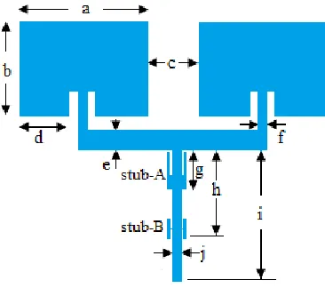
Figure 1 shows the configuration of the proposed antenna array. The antenna array is designed on an FR4 substrate of thickness 1.58 mm, dielectric constant of 4.4, and loss tangent of 0.02. This array consists of two radiating elements (patch) which have resonance at 5.2 GHz. The width (a) and length (b) of the patches are calculated using the standard design formula of microstrip patch antenna [12], which is further optimized to get the desired responses. The patches are excited by a microstrip feed network which is defined by parameters ‘e’, ‘f’, ‘i’ and ‘j’. Two pairs of open-ended stubs (pair of stub
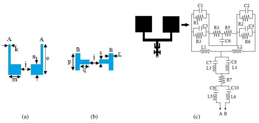
A and pair of stub B) are integrated with the array, and their larger views are shown in Fig. 2. Stub ‘A’ is defined by ‘k’, ‘m’, ‘n’, and ‘o’ whereas stub ‘B’ is defined by parameters ‘p’, ‘q’, ‘r’, and ‘s’. All the dimensions are listed in Table 1. The antenna is fed by a vertical 50 Ohms transmission line which is further divided into two 100 Ohms horizontal lines as shown in Fig. 1. These 100 ohms lines are fed to patch elements of the array.
Figure 1. Structure of the proposed antenna array.
(b)
(a) (c)
Figure 2. (a) Stub ‘A’ of vertical length (o) ≈ λg1/2 (λg1 ≈ guided wavelength of the 1st harmonic frequency and (b) Stub ‘B’ of vertical length (p) ≈ λg2/4 (λg2 ≈ guided wavelength of 2nd harmonic frequency. (c) Equivalent circuit of stub integrated array.
Figure 3. Simulated|S11|characteristic of the reference array.
Table 1. Antenna and stub dimensions (in mm).
Parameters a b c d e f
Dimension 17.5 13.1 13.8 7.2 2.6 1.4
Parameters g h s i j k
Dimension 6.8 13.325 0.2 20.275 2.025 0.325
Parameters m n o p q r
Dimension 0.6 3.525 6.75 2.425 0.2 0.5
Figure 4. Simulated|S11|characteristic of the reference array and the stub integrated array.
(b) (a)
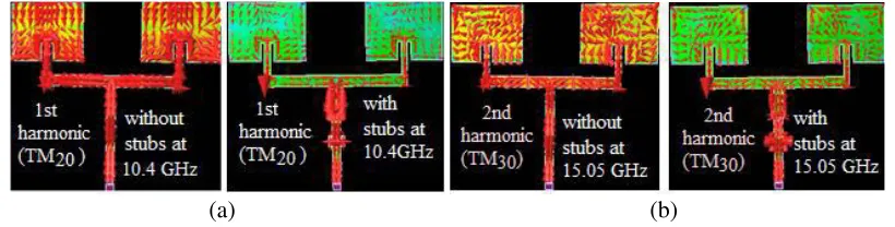
Figure 5. Simulated current distribution (a) at 10.4 GHz and (b) at 15.05 GHz. (from left without stubs and with stubs).
is chosen for stub ‘B’ as quarter of the guided wavelength of the 2nd harmonic (λg2/4) to suppress the corresponding harmonics. The simulated |S11|of the array with stubs and the array without stubs are shown Fig. 4. Effective suppression of the 1st and 2nd harmonics along with sub-harmonics is evident from this figure. The 1st harmonic is suppressed due to stub pair ‘A’ and that for 2nd harmonic is due to stub pair ‘B’ as their vertical length is half and quarter wavelength of the corresponding harmonic frequency, respectively. The simulated current distributions at 10.4 and 15.05 GHz frequencies are shown for both the cases (without stubs and with stubs) in Fig. 5(a) and Fig. 5(b), respectively. It is noticed from Fig. 5(a) that the surface current flow on the patch decreases at the 1st harmonic (10.4 GHz) when stubs are integrated compared to without stubs. The reduction of surface current flow on patch is due to large accumulation of current at stub pair ‘A’. This reduction of current flow on the patch effectively suppressed the 1st harmonic. In the same way from Fig. 5(b), the suppression of the 2nd harmonic can be explained. Furthermore, due to the combined effect of both stubs, the sub-harmonics also get suppressed. Normally, the stub has a stopband and passband. In this work, we set the passband and stopband in such a way that it passes the fundamental frequency and stops the higher order modes of propagation. The stopband and passband of the stub have been optimized by the process of simulation, and it has been observed that there is no change of the antenna characteristics after the introduction of stub (optimized). Moreover, different lengths of stub provide different stopbands and passbands. So, by using the same set of stubs different stopbands and passbands cannot be achieved.
(b) (a)
Figure 6. (a) Simulated elevation pattern views (co-pol.) of the array [f0 = fundamental, f1 = 1st harmonic andf2 = 2nd harmonic]. (b) Surface current distribution at 5.2 GHz (from left without stubs and with stubs).
(b)
(a) (c) (d)
Figure 7. Fabricated antennas (a) without stubs (b) with stub-A (c) with stub-B and (d) with both stubs.
Figure 8. Measured|S11|characteristics of the array for different configurations.
with ( ) & without stubs ( ) at 5.2 GHz, with ( )
& without stubs ( ) at 10.4 GHz and with( ) & without stubs ( ) at 15.05 GHz).
Figure 9. Measured 2D co-polar radiation patterns.
Cross polarization level with Stub at fundamental frequency 5.2GHz
Cross polarization level without Stub at fundamental frequency 5.2GHz
Co-polarization level with and without stub
at fundamental frequency 5.2 GHz.
There is a significant difference between simulated and measured patterns at 15.05 GHz. The mismatch between the simulated and measured results has occurred due to probable imperfections in the fabrication process, coupled with the possible presence of unknown parasitic effects which was not considered in the simulation process. Furthermore, hand soldering of SMA connectors may have been one of the causes of the aforesaid discrepancy.
The array cross-polarization level (in H-plane) for the fundamental frequency is shown in Fig. 10. Here co-polarization is also given for the comparison. From Fig. 10, it is observed that cross-polarization level in H-plane is very low, and the difference between co-polarization and cross-polarization levels is 47 dB. It has been observed after implementing the stub that the cross-polarization level has been increased slightly, but it is within the accepted level.
4. CONCLUSION
The higher order modes (TM01, TM11, TM20, TM12, and TM30) of fundamental frequency (TM10) are successfully suppressed in microstrip antenna array. A pair of microstrip stubs of electrical length
λg1/2, each (stub-A) placed on both sides of the feed line, results in reduction of the 1st harmonic along with some other adjacent sub-harmonics. Similarly, a pair of T-shaped stubs (stub-B) of electrical length λg2/4, each placed on both sides of the microstrip feed line, results in suppression of the 2nd harmonic along with a few other sub-harmonics. When both stubs (stub-A & stub-B) are simultaneously integrated with the feed line of the array, the harmonic signals existing in between 6–16 GHz are fully suppressed. In the present design, higher order modes are controlled by stubs only, and the limitation of the DGS or PBG structure has been overcome without degrading other parameters of antenna array. The utility of the proposed design lies in its use for WLAN applications.
REFERENCES
1. Garg, R., P. Bhartia, I. Bahl, and A. Ittipiboon, Microstrip Antenna Design Handbook, Artech House, Norwoord, 2000.
2. Horri, Y. and M. Tsutsumi, “Harmonic control by photonic bandgap on microstrip patch antenna,”
IEEE Microwave Guided Letters, Vol. 9, 13–15, 1999.
3. Chandra, U., H. F. AbuTarboush, H. S. Al-Raweshidy, and R. Nilavalan, “Wideband slotted patch antennas using EBG structures,”International Workshop on Antenna Technology (iWAT), May 13, 2010.
4. Biswas, S., D. Guha, and C. Kumar, “Control of higher harmonics and their radiations in microstrip antennas using compact defected ground structures,” IEEE Transaction on Antennas and Propagation, Vol. 61, 3349–3353, 2013.
5. Ghosh, C. K., “Harmonic suppression of microstrip antenna by using open ended stubs,”Microwave and Optical Technology Letters, Vol. 58, No. 6, 1340–1345, 2016.
6. Das Chagas Barbosa de Sena, F. and J. P. da Silva, “Harmonic suppression using optimised hexagonal defected ground structure by genetic algorithm,” IET Microwaves, Antennas &
Propagation, Vol. 12, No. 10, 1645–1648, 2018.
7. Elsheakh, D. N., M. F. Iskander, E. A. Abdallah, H. A. Elsadek, and H. Elhenawy, “Microstrip array antenna with new 2d-electromagnetic band gap structure shapes to reduce harmonics and mutual coupling,” Progress In Electromagnetics Research C, Vol. 12, 2010.
8. Pandhare, R. A., P. L. Zade, and M. P. Abegaonkar, “Harmonic control by defected ground structure on microstrip antenna array,” Indian Journal of Science and Technology, Vol. 8, No. 35, December 2015.
9. Pattapu, U., A. Gupta, and S. Das, “A 2.45 GHz harmonic suppression array antenna for rectenna application,”3rd International Conference on Microwave and Photonics, February 2018.
![Figure 6. (a) Simulated elevation pattern views (co-pol.) of the array [harmonic andf0 = fundamental, f1 = 1st f2 = 2nd harmonic]](https://thumb-us.123doks.com/thumbv2/123dok_us/7735006.1266624/5.612.171.449.471.649/figure-simulated-elevation-pattern-views-harmonic-fundamental-harmonic.webp)

