ABSTRACT
JIN, ZHANG. Frequency Agile RF/microwave Circuits using BST Varactors. (Under the direction of Amir Mortazawi)
The research has focused on characterizing barium strontium titanate or BST film at
RF/microwave frequencies, improving BST capacitor quality factors and designing
frequency agile RF/microwave circuits.
A simple and fast measurement technique is developed to extract BST loss tangent and
dielectric constant in a parallel plate BST capacitor. An error analysis is performed to
indicate the measurement accuracy. In addition, the BST capacitor layout is optimized to
achieve the best possible quality factor.
BST capacitor based tunable band-pass filters are designed. Two coupled
half-wavelength microstrip resonators are used in the filter. BST capacitors are placed at the end
of the resonators. Analysis shows that with the increase in BST capacitance, the filter skirt
sharpness increases, the circuit size decreases, and the tunability increases but the insertion
loss increases. Different filter specifications are achieved by using various BST capacitances.
In addition, a new topology is developed to maintain the 3-dB bandwidth of filters within the
tuning frequency range. The bandwidth change decreases from 54% to only 4% using the
new topology.
A tunable microstrip antenna is designed, fabricated and measured. Multiple varactors are
used to load a rectangular microstrip antenna. A figure of merit is defined to find the
optimum number of varactors. Good tunability of 25% and maximum gain of 7.8 dB are
obtained. The measurement results prove that tunable microstrip antennas using
multiple-varactor loading can achieve better performance than those using single-multiple-varactor loading.
A tunable high impedance surface is designed, fabricated and measured. The surface uses
lumped elements to form multiple parallel resonant circuits. Unlike other lumped-element
high impedance surfaces, the inductance in this surface is obtained from the grounded
substrate, which shows much higher quality factor and requires less substrate height than
those using vias to obtain the inductance. Measured tunability of 62% is achieved.
A novel digital phase shifter design at X-band is presented. The phase shifter operates
based on converting a microstrip line to a rectangular waveguide and thus achieving the
phase shift by changing the propagation constant of the medium. A 3-bit phase shifter has
been designed and constructed using PIN diodes as switches. An average insertion loss of
FREQUENCY AGILE RF/MICROWAVE CIRCUITS
USING BST VARACTORS
by
Zhang Jin
A dissertation submitted to the Graduate Faculty of
North Carolina State University in partial fulfillment of the requirements for the Degree of
Doctor of Philosophy
Electrical and Computer Engineering
Raleigh
2003
APPROVED BY:
_______________________
Prof. Amir Mortazawi (Chair)
_______________________ _____________________
Prof. Angus Kingon Prof. Jon-Paul Maria
BIOGRAPHICAL SUMMARY
Zhang JIN received the B.Sc degree in 1994 from the University of Electronic Science
and Technology of China, the M.Eng from National University of Singapore in 2000, and the
PhD from North Carolina State University in 2004. From 1994 to 1997, she worked as a
research engineer at Chengdu Institute of Technology. Her research interests include
ACKNOWLEDGEMENTS
I would like to express my gratitude to my husband, Liu Li, my parents, Jin Gongwang
and Zhang Manjing, and my sister and brother-in-law, Jin Jing and Liu Jin. Without their
encouragement, patience, and sacrifice this work would not be possible.
I would like to thank my advisor Prof. Amir Mortazawi for his guidance during my
graduate studies. I would also like to thank Prof. Angus Kingon, Prof. Jon-Paul Maria, Prof.
Gianluca Lazzi, and Prof. Griff Bilbro for their valuable suggestions and serving on my Ph.D
committee.
Many thanks go to my past and present graduate student colleagues, Sean Ortiz, Mete
Ozkar, Xin Jiang, Ayman Al-zayed, Ali Tombak, Navin Gupta, Lora Schulwitz, Jonghoon
TABLE OF CONTENTS
LIST OF FIGURES
………...……….…………...viiLIST OF TABLES
…………....………....xiLIST OF APPENDICES
....………...…....xiiCHAPTER 1 INTRODUCTION ... 1
1.1 Motivations ... 1
1.2 Overview of current technologies for continuous tunable circuits ... 2
1.3 Overview of BST thin film process for high frequency applications ... 3
1.3.1 BST composition ...4
1.3.2 BST deposition on various materials ...4
1.3.3 BST film thickness...5
1.3.4 BST process temperature ...6
1.4 Previous work in RF and microwave circuits using BST ... 6
1.4.1 BST tunable capacitors ...6
1.4.2 BST tunable filters ...7
1.4.3 BST phase shifters ...8
1.4.4 BST tunable antennas ...9
1.5 Research objectives and dissertation organization ... 9
1.5.1 Optimization of BST capacitor layout to achieve high Q factor ...10
1.5.2 Characterization of BST film at RF and microwave frequencies ...10
1.5.3 Tunable integrated filters ...10
2.1 Introduction... 13
2.2 Quality factors of BST capacitors... 14
2.2.1 Integrated BST capacitors...17
2.2.2 Discrete BST capacitors...22
2.3 BST thin film characterization... 26
2.3.1 Measurement technique for BST loss tangent and dielectric constant extraction...26
2.3.2 Error analysis on BST loss tangent measurement...30
2.4 Conclusion ... 31
CHAPTER 3 TUNABLE INTEGRATED FILTERS... 32
3.1 Introduction... 32
3.2 Capacitively loaded resonators ... 32
3.3 Tunable band pass filter design using capacitively loaded resonators ... 40
3.4 Design of tunable filters with constant bandwidth ... 44
3.5 Conclusion ... 45
CHAPTER 4 TUNABLE MICROSTRIP ANTENNA... 46
4.1 Introduction... 46
4.2 Advantages of using multi-varactor loading... 47
4.2.1 Radiation pattern improvement...49
4.2.2 Antenna gain improvement...50
4.3 Design of tunable antenna using multi-varactor loading ... 53
4.3.1 Tunability...53
4.3.2 Figure of merit ...56
4.4 Measurement results ... 57
4.5 Conclusions... 60
CHAPTER 5 TUNABLE ARTIFICIAL HIGH IMPEDANCE SURFACE ... 62
5.1 Introduction... 62
5.2 Theory of artificial high impedance surface ... 63
5.3 Tunable high impedance surface design ... 69
5.4 Fabrication and measurement ... 77
5.6 Conclusion ... 80
CHAPTER 6 DESIGN OF A NEW DIGITAL PHASE SHIFTER AT X-BAND... 81
6.1 Introduction... 81
6.2 Background... 81
6.3 Theory... 83
6.4 Experimental results... 88
6.5 Conclusion ... 93
CHAPTER 7 CONCLUSIONS... 94
APPENDIX A ... 96
LIST OF FIGURES
Figure 2.1 Skin depth of the thin film platinum... 14
Figure 2.2 Conductor (Qm), dielectric (Qd) and total quality factors (Qt) as a function of frequency... 15
Figure 2.3 (a) Integrated and (b) discrete BST capacitors ... 16
Figure 2.4 The current distributions of (a) the capacitor and (b) the equivalent electrode. 18 Figure 2.5 Simulated current distributions of BST capacitor ... 18
Figure 2.6 (a) the distributed and (b) one-stage equivalent circuit model of the capacitor 19 Figure 2.7 Normalized R’s at different capacitor dimensions. ... 21
Figure 2.8 Normalized Rbot at different sizes of bottom electrode... 22
Figure 2.9 Current distributions on a discrete capacitor ... 23
Figure 2.10 Figure 2.10 Normalized R’s at different capacitor dimensions... 24
Figure 2.11 Normalized Rbot at different sizes of bottom electrode... 24
Figure 2.12 Normalized R’s at different bonding positions... 25
Figure 2.13 Normalized R’s at different bonding diameters... 25
Figure 2.14 (a) the BST capacitor and standards (b) short #1 and (c) short #2 are fabricated on the same wafer ... 27
Figure 2.15 Equivalent circuits of the on wafer (a) capacitor, (b) short #1 and (c) short #2 28 Figure 2.16 BST capacitance and loss tangent versus frequency ... 29
Figure 2.17 Standard deviation of measured loss tangent versus frequency ... 31
Figure 3.1 Half wavelength resonator and its current and voltage distribution... 33
Figure 3.2 (a) Folded half wavelength resonator, and (b) folded half wavelength resonator with reduced size by using a tunable capacitor connecting at the two ends ... 34
Figure 3.3 (a) BST capacitor loaded resonator and (b) its equivalent circuit ... 34
Figure 3.4 Zeros and poles of resonators with and without loaded capacitor... 36
Figure 3.5 Relative distance between zero to pole as a function of Cbst... 37
Figure 3.6 Zero and pole of input impedance for capacitively loaded resonator as a function of loading capacitance ... 38
Figure 3.8 (a) a conventional two-pole hairpin filter consisting of two coupled half
wavelength resonators (b) hairpin filter with two coupled BST capacitor loaded
resonators ... 40
Figure 3.9 Filter response at over, under and critical coupled condition... 41
Figure 3.10 Simulated S-parameters of the band pass filters (a) design #1, Cbst=2.5 pF and (b) design #2, Cbst=1 pF ... 42
Figure 3.11 BST tuned hairpin filter with constant bandwidth design ... 44
Figure 3.12 Simulated S-parameters of the bandpass filter with constant bandwidth design ... 45
Figure 4.1 Microstrip antenna... 47
Figure 4.2 (a) single and (b) multiple varactor tuned microstrip antenna ... 48
Figure 4.3 The electrical field distribution along radiating edge and the radiation pattern at different bias voltage for (a) single varactor tuned and (b)multiple varactor tuned microstrip antenna... 49
Figure 4.4 (a) multiple varactor loaded radiating edge and its equivalent circuit (b) multiple varactors simplified as one effective varactor and its equivalent circuit ... 50
Figure 4.5 Antenna gain for a multiple and single varactor loaded antenna ... 53
Figure 4.6 (a) multiple varactor loaded antenna evenly divided by n cells where n is the number of varactors at each radiating edge (b) current distribution for each unit cell... 54
Figure 4.7 Antenna tunability as a function of loading capacitance C1... 55
Figure 4.8 Plot of figure of merit for the antenna as a function of number of varactors used ... 56
Figure 4.9 Picture of fabricated microstrip antenna with four varactors loading at each radiating edge... 57
Figure 4.10 Measured S-parameter of antenna ... 58
Figure 4.11 Setup for antenna radiation pattern and gain measurement... 59
Figure 4.12 Measured (a) E-plane and (b) H-plane of antenna radiation pattern ... 60
Figure 5.1 Conventional high impedance surface using corrugated metal slab whose
grooves are λ/4 from the bottom ground ... 63
Figure 5.2 Lumped-element based high impedance surface using vias to create inductance (a) top view (b) side view ... 64
Figure 5.3 (a) Origin of the capacitance and inductance in the high impedance surface (b) the equivalent circuit of the high impedance surface... 65
Figure 5.4 EM wave incident upon and reflected from a grounded dielectric substrate .... 66
Figure 5.5 Comparison of quality factors for a 5 nH inductor using grounded dielectric substrate and vias ... 68
Figure 5.6 Required height of via and grounded dielectric substrate for different inductance values ... 68
Figure 5.7 Modified high impedance surface structure using grounded dielectric substrate with no vias inside (a) top view (b) side view ... 69
Figure 5.8 (a) Tunable high impedance surface using varactors at the gap between two pads (b) equivalent circuit of the tunable high impedance surface... 70
Figure 5.9 (a) Equivalent circuit of high impedance surface with parasitics (b) simplified equivalent circuit... 71
Figure 5.10 (a) a shorted lossy transmission line and (b) its equivalent circuit using a same length lossless transmission line and a series impedance ... 72
Figure 5.11 Rc , RL and Rp as a function of Lsub /Cvar... 74
Figure 5.12 Bandwidth definition of high impedance surface... 74
Figure 5.13 Bandwidth of the high impedance surface as a function of Lsub/Cvar... 75
Figure 5.14 Bias network for the tunable high impedance surface... 76
Figure 5.15 Photograph of the high impedance surface ... 78
Figure 5.16 Measurement setup for the high impedance surface ... 78
Figure 5.17 Measured phase of reflection coefficient calibrated at the surface of high impedance structure ... 79
Figure 5.18 Rectangular waveguide phase shifter with tunable high impedance surfaces placed at the two side walls ... 80
Figure 6.2 Perspective and frontal views of the phase shifter with PIN diodes used as switches... 84 Figure 6.3 Phase shift as a function of operating frequency... 85 Figure 6.4 Electric field distribution for the (a) microstrip and (b) waveguide... 86 Figure 6.5 Waveguide impedance as a function of waveguide width a (b=15mil,εr =6
and f =10 GHz)... 87 Figure 6.6 Photograph of the 3-bit phase shifter... 89 Figure 6.7 The equivalent circuit of the PIN diode under (a) forward bias and (b) reverse
bias. ... 89 Figure 6.8 The cutouts near the diode to compensate the diode capacitance under reverse
bias. ... 90 Figure 6.9 (a) Simulated and (b) measured phase shift of the 3-bit phase shifter. ... 91 Figure 6.10 (a) Simulated and (b) measured return and insertion loss of the 3-bit phase
LIST OF TABLES
LIST OF APPENDICES
CHAPTER 1
INTRODUCTION
1.1
Motivations
With the rapid growth of communication systems including satellite, bluetooth, 3G
wireless phone, ultra-wide band (UWB) and optical network, it is desirable to be able to
design frequency agile RF front ends for operation in various frequency bands. Tunable RF
and microwave components are thus in largely demanded due to their frequency agile
characteristics. In addition, high-speed, small-size, and low-operation voltage components
are required in the current and next generation communication systems. These requirements
impose significant challenges on current tunable circuit technologies and illustrate the need
for new materials, technologies and designs. Barium strontium titanate ( (Bax,Sr1−x)TiO3) or
BST, a ferroelectric film whose dielectric constant can be controlled by the application of a
DC electric field, has shown great promise for the design of tunable RF and microwave
circuits such as phase shifters, filters, antennas, adaptive matching circuits, and
voltage-controlled oscillators. Therefore, the main objectives of this research work are to characterize
BST film and capacitors at RF and microwave frequencies and develop novel frequency agile
1.2
Overview of current technologies for continuous tunable circuits
There are currently five existing technologies for the design of continuous tunable
circuits based on mechanical tuning, ferrite, MEMs, semiconductor varactors and
ferroelectric materials. The earliest forms of tunable circuits were all mechanical, for
example, the rotary vane adjustable waveguide phase shifter first proposed by Fox in 1947
[1]. Mechanical circuits are cheap, simple to fabricate and have very low loss. However their
disadvantages include their large size and low tuning speed. In 1957 Reggia and Spencer
reported the first electronically variable ferrite phase shifter [2]. Ferrite can handle large
power levels and has faster switching time (few µs to tens of µs) than mechanical ones.
However, ferrite based circuits also have large size and mass, and need tunable magnetic
fields to operate. In the 1960s, semiconductor diodes were introduced in tunable circuits and
are still the dominant devices for making tunable circuits [3][4]. They are very small (in
µms), very fast (<1µs for pin diode and <1 ns for FET), and have large tunability (3:1~10:11
or 200%~900%). In addition, they can be easily integrated with other circuits for example in
monolithic microwave integrated circuits (MMICs). However, semiconductor based varactors
suffer from the junction noise and have poor power handling capability. Also, they require
reversed bias to keep them capacitive. This is a potential problem of semiconductor varactors
operating under large RF signals because the varactor diodes might be turned on (act as a
resistor) if the signal voltage amplitude is larger than the reverse bias. In early 1990s, MEMs
were started to use for tunable circuits [5]. MEMs have very little loss at RF and microwave
frequencies and can handle higher power levels. However, they have some disadvantages
including low tunability (<1.5:1, or 50%), slow switching speed (2-100 µs), and high bias
voltage (50-100 V). In addition, they require hermetically sealed packaging, which is
expensive and hard to integrate with other circuits. Another alternative approach for making
tunable devices is to employ ferroelectric based varactors. They are fast, low loss at RF and
microwave frequencies, and can handle more power than semiconductor varactors. Their C-V
curve is symmetric with respect to the bias voltage, thus there is no requirement for reverse
bias like semiconductor varactors. They can be used in bulk form so that planar circuits like
coplanar waveguide and microstrip lines can be directly fabricated on them. In addition, they
can be used in parallel plate or interdigital capacitors, which can be integrated in other
circuits. The recent results obtained from ferroelectric varactors indicate their potential for
making tunable RF front ends.
Strontium titanate, SrTiO3 (STO) and BST are two of the most popular ferroelectric films
currently being studied for the design of tunable RF circuits [6]-[16]. Tunable STO
characteristics can be obtained only at low temperatures thus allowing the use of high
temperature superconductors (HTS) to achieve lower loss. However, since STO exhibit very
little tunability at room temperature, they cannot be employed in systems operating at room
temperature. BST films can overcome these difficulties. Depending on the specific
composition, BST can exhibit paraelectric behavior and making it tunable at room
temperature (typically 2:1 or 100% tunabilities are reported). With the recent advances in
BST thin film deposition and processing, low loss tunable capacitors, filters, phase shifters
and antennas requiring lower drive voltages can be fabricated.
The electrical characteristics of BST thin films greatly depend on the BST composition,
the bottom electrode materials, the film thickness, and the process temperature. Researchers
from different groups have studied these properties.
1.3.1 BST composition
The BST properties are varied by the composition of Ti and Ba/Sr ratio. The Ti content is
studied from 51.5% to 55.0% by our group [13]. The result showed that the loss tangent and
tunability decreased when increasing the excess of Ti content. For 55.0% Ti and thickness
≤700 Å, BST thin films reached loss tangent as low as 0.003. The figure of merit, which
combines the information of loss tangent and tunability, showed that BST film with 53.3% of
Ti content gave a good compromise between a low loss tangent and a relatively high
tunability.
The dielectric constant can be tuned by adjusting the Sr content of the base composition.
For compositions with ≥35 mol% Sr, BST is cubic at room temperature and hence exhibits
paraelectric behavior [17]. Studies showed that the BST film has a higher dielectric constant
with a lower Sr content.
1.3.2 BST deposition on various materials
The electrodes deposition in parallel plate capacitor structures are challenging, especially
for the bottom electrode. It must provide good growth surface for BST and be stable at high
growth temperatures in an oxidizing atmosphere yet have high conductivity and be
compatible with substrates. BST thin films have been tried to deposit on different metals
capacitors. However, the BST growth prevents the use of Pt thickness over 0.1-0.2 µm [19],
which is smaller than the skin depth up to 2000 GHz2. This turns out to be the main factor that limits the total quality factor of the BST capacitors. Multi-layer bottom electrode
structure, which includes adhesion and interleaved barrier layers were investigated,
fabricated and measured by our group [19]. We successfully increased the pure Pt electrode
up to 0.5 µm, and thus increased the total quality factor of the BST capacitors.
BST thin films have been also deposited directly on dielectric materials including MgO
[20]-[23], LaAlO3 [21] [22] and sapphire [15]. Silicon is also used as the substrate for BST
[24]. The BST showed tunability with the applied DC voltage and reasonable loss tangent on
these materials. However, due to the lack of one metal layer, capacitors must be in the
interdigital form, which require high bias voltage (200-300V), and have less tunability since
the electrical field goes partially to the air.
1.3.3 BST film thickness
BST characteristics are strongly depended on the film thickness [13]. Our group reported
that the dielectric constant rises with film thickness. We have also observed that the loss
tangent increases with the film thickness up to 4000-5000 Å, and then drops slightly with
further increase in film thickness. However, the tunability decreases with film thickness up to
3000-4000 Å, and then slightly rises with further increase in film thickness (BST thin films
were deposited by a liquid-delivery-source CVD technique at approximately 640°C,
Ba/Sr=70/30) [13].
2 Skin depth
ωµσ
1.3.4 BST process temperature
The substrate temperature during growth has a very strong influence on electrical and
physical properties of BST films [14]. A high growth temperature promotes formation of
more highly crystalline material, while at low temperatures microcrystalline or amorphous
material is formed [14]. The measurement results reported by our group indicates that the
dielectric constant increases with the rise of growth temperature.
1.4
Previous work in RF and microwave circuits using BST
1.4.1 BST tunable capacitors
There are basically two types of capacitors, interdigital and parallel plate. Interdigital
capacitors have smaller tuning range but are easy to fabricate (only have one metal layer) and
capable of high power operation due to their large area and higher bias voltage requirement.
Parallel plate capacitors can achieve maximum tunability at low power levels but have one
more metal layer than the interdigital capacitors. For both types of capcitors, the total quality
(Q) factor is dominated by the thin electrodes of the capacitors
[11][12][15][16][19][25]-[27]. Various approaches for increasing the thickness of the electrodes are being developed.
One of the biggest challenges for depositing thicker electrodes is to find suitable conductor
stacks for the parallel plate capacitor bottom electrodes that will survive the high growth
temperatures of BST, and maintain good adhesion during the subsequent processing. We
have tested several samples using multi-Pt layers with TiAlN or IrO2 as the adhesion or the
interleaved barrier [19]. Results showed that while TiAlN worked well as a sticking layer for
adhesion and an interleaved barrier layer, allowing successful formation of BST capacitors
on bottom electrodes as thick as 2 µm. It was also found that as little as one barrier layer
placed near the top of the Pt structure, it provided adequate protection for the multi-layer
bottom electrode. BST dielectric constants ranging from 150-400 (depending on film
thickness) and tunability of approximately 2:1 (100%) were achieved on these thick bottom
electrodes. The loss tangent of BST film was found to be less than 0.006 (±0.002) between
45 and 200 MHz [19]. Using this process, the total Q factor for a 310 pF parallel plate
capacitor with 1 µm multi-layer bottom electrode and 0.7 µm top electrode (Pt) was 77 at 50
MHz. In addition, the tunability of 2.4:1 (138%) at 5 V was obtained. To the best of our
knowledge, this is the highest quality factor for a 300+ pF tunable capacitor available in the
market.
York’s group has reported Pt on sapphire substrate [15], and Ti/Pt/Au electrode stacks
[16] on glass substrates for interdigital capacitors. They reported an interdigital capacitor of 7
pF with the tunability of 1.75:1 (75%) and Q factor of larger than 20 from 0 to 24 GHz at 90
V [15]. They also reported a 0.15-2 pF parallel plate capacitor with tunability of 2:1 (100%)
and Q factor of 30 at 20 GHz [26]. So far, these are the highest quality factors reported for pF
size BST capacitors at 20 GHz.
1.4.2 BST tunable filters
BST-based low pass and band pass filters were reported by our group [12] in 2001. The
circuits used lumped inductors and tunable BST capacitors forming a 3rd and 5th order 0.5 dB ripple Chebychev prototype low pass filter and a 3th order band pass filter at VHF frequencies. The parallel plate BST capacitors were fabricated on 500 µm thick silicon wafer
technique was used to grow the 3000 Å thick (Ba0.7Sr0.3)TiO3 thin films. The Q factor of the
32 pF BST capacitors was 50 at 160 MHz. For the 3rd order low pass filter, the maximum
measured insertion loss in the pass-band was 0.8 dB and return loss better than 10 dB. The 3
dB cut-off frequency was tuned from 160 MHz to 210 MHz (30% tunability) with 9 V bias.
For the 5th order low pass filter, the tunability reached 40%. The insertion loss of the band pass filter was 7 dB at 0 V and was reduced to 5.1 dB at 10 V. A 45% tunability was
obtained. Note that most of the insertion loss (4.5 dB of 7 dB) was found from the low Q
factor of the inductors.
In the mean time, Paratek Microwave Inc. has commercialized two types of BST-based
band pass filters, including the hybrid microstrip line resonator filter at 2 GHz [28], and the
finline waveguide resonator filters at 22.5 and 38.5 GHz [29]. The first one is a 4-pole
microstrip combline bandpass filter with tunable BST capacitors. The insertion loss at the
pass band was 7.7 dB at 200 V, the center frequency can be tuned from 2.16 to 2.36 GHz
(9.3% tunability). The two-pole finline filter has the insertion loss of 3 dB at 38.5 GHz and a
small tunability of 1% at 200 V. The three-pole finline filter operates at 22.5 GHz, and the
maximum insertion loss was only 2 dB. The tunability of 2.2% is achieved with 300 V bias
voltage. The BST tunable capacitors used in these filters were thick film (8 µm thick BST
film) interdigital capacitors, which required high DC bias voltage. The thick films were
deposited on the 20-mil thick MgO, and the gold was used as the electrodes. There was no
report on the dielectric constant and loss tangent of these BST films.
1.4.3 BST phase shifters
gel technique. A phase shift of 165° was obtained at 2.4 GHz with insertion loss of below 3
dB by using a bias voltage of 250 V. In 1999, Van Keuls reported a thirteen- section Ku-band
coupled microstrip phase shifter [23], which used BST interdigital capacitors as the series
coupling components. A phase shift of 200° was obtained at 14 GHz with insertion loss of
below 4.7 dB by using a bias voltage of 400 V. York has reported several phase shifters
using parallel plate and interdigital BST capacitors [15][16][26][30]. The BST capacitors
were used in a as the periodically loaded CPW line. The best performance for the phase shift
of 240° was obtained at 10 GHz with insertion loss of below 3 dB at a bias voltage of 17.5 V
[31].
1.4.4 BST tunable antennas
A microstrip antenna consisting multi-dielectric layer structure with thin BST
sandwiched between two dielectric slabs was investigated in [32]. In this paper, the BST has
the dielectric constant varied from 1800 to 9000, which caused the null of H-plane radiation
pattern to move from 16º to 85º. The author did not report the change of the resonant
frequency.
1.5
Research objectives and dissertation organization
The research on BST has been going on for more than a decade. However, there are still
many challenges to overcome. For example, the properties of BST thin film alone (the
material properties excluding electrode) in the capacitor form have not been accurately
obtained at microwave frequencies, and the electrical means of improving the total Q have
not been implemented. Furthermore, the designs of microwave tunable circuits using BST
capacitor layout to obtain best Q to accurately characterize BST film at RF and microwave
frequencies and to develop novel frequency agile circuits using BST. This work includes the
following five areas:
1.5.1 Optimization of BST capacitor layout to achieve high Q factor
In order to obtain high Q BST capacitors, material scientists have put much effort to
increase the electrode thickness, which is still the most critical and challenging task in the
fabrication of high Q BST capacitors. Besides from improvement in electrode properties, the
quality factor can also be improved by choosing the optimum layout for the capacitors, which
can substantially affect the Q factor. One of the goals in this work is to study the current
distribution in parallel plate capacitors, and to propose suitable layout for achieving highest
possible Q.
1.5.2 Characterization of BST film at RF and microwave frequencies
Accurate and fast characterization of BST thin film can help material scientists to
optimize the film growth condition and also provide important information about key devices
in a tunable circuit. However, due to the high loss of the electrodes, it is very hard to
accurately extract the BST characteristics. The goal in this work is to develop a new and
simple measurement technique to accurately determine the dielectric constant and loss
tangent of BST thin film at RF and microwave frequencies.
1.5.3 Tunable integrated filters
Electronically tunable filters with fast tuning speed and narrow bandwidth are required
microstrip line resonators are investigated. Filters with low loss, high tunability, and small
size are designed. In addition, a common drawback of tunable filters is their bandwidth
change with frequency, which is normally not desired. In this work, new filter topology is
developed to achieve constant bandwidth.
1.5.4 Tunable antennas
Microstrip antennas are widely used in wireless communication systems because they are
lightweight, compact, conformable to planar and non-planar surfaces, simple and inexpensive
to manufacture using modern printed-circuit technology. However, the main disadvantage of
microstrip antennas is their narrow operation bandwidth. In situations when there is no need
for high instantaneous bandwidth, like frequency hopping in cell phone systems, one can
improve the operating frequency range of antennas by making them tunable. Microstrip
antennas with multiple-varactor loading at the radiating edges are designed, fabricated and
measured. This type of tuning can achieve more tunability than using multi-dielectric layers
with BST in between. In addition, constant radiation patterns and improved 2-3 dB gain are
achieved by using multiple varactors.
1.5.5 Tunable high impedance surfaces
A high impedance surface has properties that are opposite to normal metal surface which
has low surface impedance. It does not allow ac current to flow on the surface and thus does
not support surface waves. In addition, the image currents due to high impedance surface are
not phase reversed, therefore they can be used as antenna reflectors without affecting the
radiation efficiency. The surface can be described using photonic band gap (PBG) concepts
developed, which uses the basic non-tunable design in [34] with further modification to
improve loss and simplify the fabrication.
In the dissertation, chapter 2 reports the characterization of BST film which includes the
quality factor improvement and measurement techniques to obtain loss tangent. Tunable
filters, antennas and high impedance surfaces are described in chapters 3, 4 and 5
respectively. In chapter 6, a new phase shifter design is presented. The dissertation is
CHAPTER 2
CHARACTERIZATION OF BST
CAPACITORS
2.1
Introduction
One of the most important parameters for a capacitor, which indicates the loss is its
quality factor defined as
CR
Q=1/ω (2.1) where, ω is the angular frequency, C is the capacitance and R is the equivalent series resistance. R represents the total loss in a capacitor, which includes metal and dielectric
losses. In this chapter, major loss sources in a parallel plate form are examined and various
capacitor layouts are simulated and optimized to achieve the best possible Q. In addition, it is
important to be able to determine the loss tangent of the dielectric material (here BST thin
film) in a capacitor in order to optimize the material growth process. A quick and accurate
measurement technique is developed to extract the loss tangent of BST film in a parallel plate
2.2
Quality factors of BST capacitors
The total quality factor of the BST capacitors is determined by two different loss
mechanisms, the conductor loss due to the electrodes and the dielectric loss from the BST
thin film. It can be expressed as:
d m
t Q Q
Q
1 1
1 = +
(2.2)
where, Qt is the total quality factor,
m m
CR Q
ω
1
= is the conductor (electrode) quality factor
(Rm: equivalent resistance of the electrodes), and
δ
tan 1 = d
Q is the dielectric (BST) quality
factor. Since the electrode thickness (normally 0.1~0.2 µm) is much less than the skin depth
(up to 100 GHz), as shown in Figure 2.1, Rm remains almost constant (same as its DC value)
at microwave frequencies.
Figure 2.1 Skin depth of the thin film platinum
(σ=3e+6 S/m)
205.57
65.01
20.56
6.50 2.06 0.65 0.00
50.00 100.00 150.00 200.00 250.00
1 10 100 1000 10000 100000
Frequency (MHz)
S
ki
n
de
pt
h
(u
m
Figure 2.2 Conductor (Qm), dielectric (Qd) and total quality factors (Qt) as a function of frequency
(C=5 pF, tanδ=0.005)
Figure 2.2 shows the contribution of the conductor and dielectric quality factors to the
total Q for a 5 pF capacitor. It can be seen that the conductor Q dominates at high frequencies
(>1 GHz). Therefore, focuses must be on Rm in order to increase the total Q of BST
capacitors. To reduce Rm, the most obvious way is to increase the electrode thickness, d, as
Rm is proportional to 1/d. However, due to the difficulties associated with increasing the
electrode thickness [19], other solutions that do not rely on thick electrodes need to be
investigated. Among these is the effect of capacitor layout on Rm. The capacitor layout is
investigated on two different implemented capacitors, integrated and discrete capacitors as
shown in Figure 2.3. Both types of capacitors can be used in tunable circuits. Integrated
capacitors can be fabricated together with other parts of circuit while discrete capacitors are
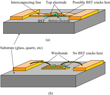
fabricated on a separate wafer and must be diced before wire bonded. In integrated
capacitors, there are possible BST cracks along the edges of the bottom electrode as shown in 0.10
1.00 10.00 100.00 1000.00 10000.00 100000.00
10 100 1000 10000 100000
Frequency (MHz)
Q
u
al
it
y f
act
o
r
Figure 2.3 (a), which might cause the capacitor failure. On the other hand, discrete capacitors
are easier to fabricate and are more reliable. Integrated capacitors can be much smaller than
discrete capacitors (usually larger than 7 pF based on BST thickness=700 Å, εr=200,
size=17×17 µm2), which may not be suitable for RF/microwave applications, but can be used
for IF (inter-medium frequency, 50-200 MHz) applications. In the following section, the
current distributions of both types of capacitors are studied.
Figure 2.3 (a) Integrated and (b) discrete BST capacitors (a)
(b)
Top electrode
BST Bottom electrode
Interconnecting line
Wirebonds
Possible BST cracks here
2.2.1 Integrated BST capacitors
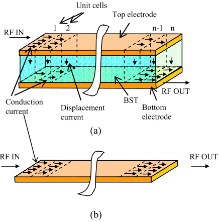
Figure 2.4 shows the current distribution of the integrated BST capacitor. The total RF
current flowing into the capacitor consists of the conduction and displacement current
(Figure 2.4a). Conduction current flows on the surface of the electrode and displacement
current flows into the dielectric with direction vertical to that of the conduction current. As
conduction current flows, part of it is converted to displacement current. When displacement
current reaches the bottom electrode, it changes back to conduction current and flows along
the bottom electrode. Therefore, the density of conduction current along the capacitor
electrodes varies. On the top electrode, the conduction current density is maximum at the
“RF IN” terminal, and decreases to zero (or very small value if fringe fields are not
neglected) at the end of top electrode. While on the bottom electrode, it is zero at the
beginning and increases to its maximum at the “RF OUT” terminal. In addition, as the
dimension of the capacitor is much smaller than the operation wavelength (<0.01λ up to 100
GHz) the voltage along the electrode can be regarded as a constant. Therefore electrical field
density is uniform in the dielectric, which implies that the displacement current density is
also uniform since
E j
Jd = ωεr (2.3)
where Jd is the displacement current density, ε is the permittivity and Er is the electric
field in the dielectric. The capacitor is simulated using a commercial 3-D EM simulator
Figure 2.4b shows an electrode having the same dimensions as the capacitor electrode
(equivalent electrode). The conduction current on the equivalent electrode flows uniformly
since there is no displacement current involved.
Figure 2.4 The current distributions of (a) the capacitor and (b) the equivalent electrode
Figure 2.5 Simulated current distributions of BST capacitor
Conduction current
Displacement current
L
W
RF OUT RF IN
(b)
Unit cells
(a)
Conduction current
1 2 n-1 n RF IN
RF OUT Top electrode
Bottom electrode BST Displacement current
Thus the resistance of the capacitor electrode is different from a same shape equivalent
electrode. To find the relation of the resistance and inductance between these two, a
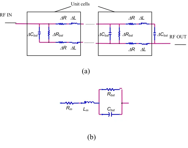
distributed model as shown in Figure 2.6 (a) is used. The one-stage lumped-element
equivalent circuit is shown in Figure 2.6 (b). As indicated in Figure 2.4 (a), the capacitor is
divided into n small cells along the electrode.
Figure 2.6 (a) the distributed and (b) one-stage equivalent circuit model of the capacitor
The equivalent circuit of each cell consists of a small series resistance (∆R) and inductance (∆L) for the top and bottom electrodes, and a small shunt capacitance (∆Cbst) and
resistance (∆Rbst), which are given by:
n R R= eq_elec
∆ (2.4)
n L L= eq_elec
∆ (2.5) (b)
Lm
Rbst
Cbst Rm
(a)
RF IN ∆R ∆L
∆R ∆L
∆Cbst ∆Rbst
∆R ∆L
∆R ∆L
∆Cbst ∆Rbst ∆Cbst RF OUT
1
+ = ∆
n C
C bst
bst (2.6)
bst
bst n R
R =( +1)
∆ (2.7)
where, Req_elec and Leq_elec represent the total resistance and inductance of the equivalent
electrode (Figure 2.4 (b)), respectively. This distributed circuit model should be equal to the
one-stage equivalent circuit model of the capacitor shown in Figure 2.6 (a) and (b). The two
circuits are simulated in a circuit simulator (Agilent ADSTM ). The equivalent series resistance and inductance are:
Rm=2/3×Req_elec (2.8)
Lm=2/3×Leq_elec (2.9)
Lm is different from results obtained by Pucel [35].
To separate the top and bottom electrode resistance, Rm can be expressed as:
bot top
m R R
R = + (2.10)
where, Rtop and Rbot represent the equivalent resistance for the top and bottom electrodes
respectively.
Based on equation (2.8), Rtop and Rbot can be expressed as:
ρ
× × =
W L
Rtop 1
2 3 1
(2.11)
ρ ρ+ × ×
× =
W L W
L
Rbot 2 1 2
3 1
(2.12)
where, ρ is the DC sheet resistance of the conductor, L1 is the length of the top and bottom electrodes, L2 is the connecting line length at the bottom electrode, and W is the width of
Rm’s as a function of L1, L2 and W are calculated based on the above analysis. To verify
its validity, the same structure is also simulated using a two and half dimensional commercial
EM solver (HP-MomemtumTM). The simulation results agree very well with the calculation, as shown in Figure 2.7. According to the current distribution on the integrated BST
capacitors, lower Rm is obtained by shortening L1 and L2 and widening W.
Figure 2.7 Normalized R’s at different capacitor dimensions.
In addition, it is found that the size of the bottom electrode has an impact on Rbot.From
Figure 2.3(a), it can be seen that the width of the bottom electrode, Wb1, can be increased
without changing the capacitance. The increase of Wb1 can reduce Rbot because it widens the
current path on the bottom electrodes. Figure 2.8 shows the simulated Rbot at different Wb1. It
can be seen that Rbot drops almost to half of its original value when Wb1 doubles. With further
increase of Wb1, Rbot reduces slightly.
R0 is R when
L1=W=50 µm L2=20 µm, D=25 µm
0 0.5 1 1.5 2 2.5
0 0.5 1 1.5 2 2.5
L/W
R/R
0
R-calculation R-simulation Rbot-calculation Rbot-simulation Rtop-calculation
Rtop-simulation L1 L2
Figure 2.8 Normalized Rbot at different sizes of bottom electrode.
2.2.2 Discrete BST capacitors
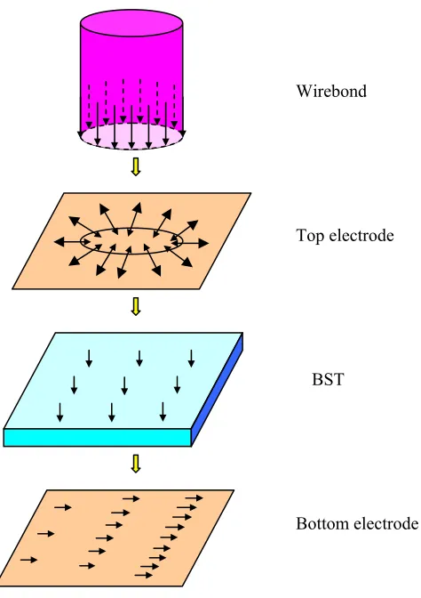
Discrete BST capacitors can be used in circuits where wirebonding is allowed. Figure 2.9
shows the total current through bond wires. The current then spreads on the top electrode,
flows through the BST as displacement current and ultimately flows through the bottom
electrode.
From Figure 2.9, it can be seen that the current distribution on the bottom electrode is the
same as that of the integrated capacitor. This is because that although the current distribution
changes on the top electrode, it can not be seen by the bottom electrode because of the
uniform displacement current in the dielectric. This is verified by the simulation results from
Agilent MomentumTM, as shown in Figure 2.10. It can also be seen from Figure 2.10 that the Rtop is much smaller than Rbot. This is because part of the top electrode is covered by the
wirebond, which effectively increases the thickness of the top electrode, thus reducing Rtop.
0 0.2 0.4 0.6 0.8 1 1.2
1 1.4 1.8 2.2 2.6 3 3.4 3.8
Wb1/W Rbot
/Rbot
0
Wb1
W
Figure 2.9 Current distributions on a discrete capacitor
In discrete capacitors, not only Wb1 but also Wb2 of the bottom electrode can be increased
without changing the capacitance, as shown in Figure 2.11. It can be easily predicted that Wb1
of the bottom electrode has the same effect on Rbot as that of the integrated capacitors, which
is verified by the simulation as shown in Figure 2.11. However, the extended size on Wb2 has
little effect on Rbot.
Top electrode
Bottom electrode BST
Figure 2.10 Figure 2.10 Normalized R’s at different capacitor dimensions
Figure 2.11 Normalized Rbot at different sizes of bottom electrode.
Results for different wirebonding positions and diameters are shown in Figures 2.12 and
2.13 respectively. The conclusion is that wirebonds should be made in the center of the
electrodes and the diameter of the wirebonds needs to be as large as possible to reduce Rtop.
As R dominates the loss in discrete capacitors, the effect of wirebond position and size is
0 0.2 0.4 0.6 0.8 1 1.2
0.4 0.5 0.6 0.7 0.8 0.9 1 1.1 1.2 1.3
L/W
R/R
0
R-simulation Rbot-simulation Rbot-calculation
Rtop-simulation L1 L2 W
D
R0 =R when
L1=W=50 µm L2=20 µm, D=25 µm)
0 0.2 0.4 0.6 0.8 1 1.2
1 1.4 1.8 2.2 2.6 3 3.4 3.8
Wb/W
Rbot /Rbot
0
Wb1 and Wb2 increase together
Wb1 increases only Wb1
Wb2
W
Rbot0 =Rbotwhen L1=Wb1=Wb2=W
Figure 2.12 Normalized R’s at different bonding positions.
Figure 2.13 Normalized R’s at different bonding diameters.
In summary, the design rules for making BST capacitors are:
For both types of capacitors, choose the minimum length for L1 and L2, and let W be
determined by the required capacitance.
For both types of capacitors, increase bottom electrode width by three times.
0 0.2 0.4 0.6 0.8 1 1.2 1.4
0.5 0.6 0.7 0.8 0.9 1 1.1
D/D0
R/R
0
R-simulation Rbot-simulation Rbot-calculation Rtop-simulation
D
R0=R when
L1=W=50 µm D0=25 µm
0 0.2 0.4 0.6 0.8 1 1.2
0.2 0.3 0.4 0.5 0.6 0.7 0.8
L/L1
R/R
0
R-simulation Rbot-simulation Rbot-calculation Rtop-simulation
L1
L
R0 =R when L=25µm L1=50
For discrete capacitors, choose the largest possible wirebond diameter and bond to the
center of the top electrode
2.3
BST thin film characterization
2.3.1 Measurement technique for BST loss tangent and dielectric constant extraction
At microwave frequencies, usually the conductor loss due to the interconnecting lines and
electrodes is a main contributor to the overall loss of thin film BST capacitors [11][26], thus
must be carefully extracted for an accurate determination of BST loss tangent. Furthermore,
the probe contact resistance increases the inaccuracy of loss tangent extraction [35]. A simple
approach is developed here to reduce these effects. In this approach, parallel plate capacitors
as well as two “short” standards are fabricated on the same wafer (Figure 2.14). Reflection
coefficient (one-port S-parameter) measurements are performed on the capacitor and the two
“short” standards individually using a vector network analyzer (VNA).
The input impedance is then obtained using:
11 11 0
1 1
S S Z Z
− +
= (2.13)
where Z0 is the reference impedance (50 Ω) of the VNA, and S11 is the reflection coefficient.
Zc, Zs1 and Zs2 represent the input impedance of the capacitor, short #1 and short #2
respectively. Zs1is used to extract the parasitics of the pads, interconnecting lines and the
discontinuities. By subtracting Zs1 from Zs2, characteristics of an equivalent electrode are
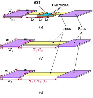
Figure 2.14 (a) the BST capacitor and standards (b) short #1 and (c) short #2 are fabricated on the same wafer
The equivalent circuits of the capacitor and two shorts are shown in Figure 2.15. Their
impedances are given by:
bst bst bst m
s c
C R j
R Z
Z Z
ω
+ + + =
1
1 (2.14)
1 1
1 s s
s R j L
Z = + ω (2.15) 2
2
2 s s
s R j L
Z = + ω (2.16) )
( 2 1
3 2
s s m
m
m R j L Z Z
Z = +
ω
= − (2.17) W1W1
W
2L1+ 2L2 +L3
W1
Electrodes BST
W1 L1 L2 L3
W
Pads
W1
W1
W
2L1+L3
Lines
(a)
(b)
where, Rs1, Ls1, Rs2 , and Ls2 are the series resistance and inductance of short #1 and short #2,
respectively. Zm is the impedance of the electrodes in the capacitor. Rbstis the shunt resistance
of thin film BST, which is given by:
δ ω tan 1 bst bst C
R = (2.18)
where Cbst is the capacitance of the two parallel plate capacitors in series, and tanδ is the
loss tangent of BST.
Figure 2.15 Equivalent circuits of the on wafer (a) capacitor, (b) short #1 and (c) short #2
BST loss tangent can be determined by removing the interconnect and electrode loss. The
error due to probe contact resistance is also reduced due to the impedance subtraction in the
loss tangent calculation. By solving equations (2.13)-(2.18) the BST loss tangent and the
device capacitance are obtained:
[
]
[
s s s c]
s s s c Z Z Z Z Z Z Z Z − − × + − × − − = ) ( Im ) ( Re tan 1 2 3 2 1 1 2 3 2 1
δ (2.19)
) tan 1 ]( ) ( Im[ 1 2 1 2 3 2 1 δ ω + × − − + = c s s s bst Z Z Z Z
C (2.20)
Rs1 Ls1 Rm Lm
Rbst
Cbst
(a)
(b) (c)
No special BST processing is required to use this measurement technique. The
measurement is performed on the devices that will be used in the actual circuits, like tunable
filters [12].
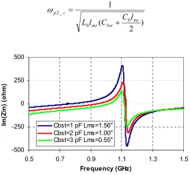
Figure 2.16 BST capacitance and loss tangent versus frequency
Figure 2.16 shows the capacitance and BST loss tangent obtained for a 0.4 pF parallel
plate capacitor. The capacitance is almost frequency independent up to 10 GHz. Thus the
permittivity of the BST film can be treated as frequency independent up to this frequency. In
addition, the BST loss tangent is also almost frequency independent. The average value of
the loss tangent is approximately 0.006 up to 10 GHz, which proves BST has potential
applications for the design of tunable RF and microwave circuits such as phase shifters,
filters and antennas.
0 0.002 0.004 0.006 0.008 0.01 0.012 0.014
0 2 4 6 8 10
Frequency (GHz)
Loss tangent
0.1 0.15 0.2 0.25 0.3 0.35 0.4 0.45 0.5
2.3.2 Error analysis on BST loss tangent measurement
In order to evaluate the accuracy of the measurement technique, an error analysis is
performed on the measured loss tangent. The goal is to calculate the standard deviation of the
measured loss tangent. It is assumed that the error is due to the uncertainty of VNA only. The
measured S parameter can be expressed as:
11 0 _ 11 11
~ S S
S = + (2.21)
where, S11_0 is the true value of S parameter and S~11 is the measurement error.
It can be assumed that the mean of S~11 is zero. Also the standard deviation of S~11 is the
uncertainty provided by the VNA datasheet [37]. The detailed derivation for the standard
deviation of measured loss tangent is in Appendix A.
A Matlab code is written to calculate the standard deviation of the measured BST loss
tangent in the 0.4 pF capacitor, and the result is shown in Figure 2.17. It can be seen that the
error is frequency dependent, and reaches its minimum when 1/ωC≅50 Ω. This is because that VNA’s impedance is 50 Ω and therefore has the minimum error when DUT is close to
50 Ω. Based on this, depending on the frequency, at which BST loss tangent should be
determined, one need to choose a capacitance value which provides close to 50 Ω reactance.
For example one can use a larger capacitor to get accurate low frequency loss tangent data
and a smaller capacitor for accurate high frequency loss tangent. Figure 2.17 also shows that
from 4.5 to 8 GHz the measurement error for loss tangent error is around 0.003. Therefore
the true value of loss tangent is around 0.006±0.003 from 4.5 to 8 GHz. The discontinuity in
Figure 2.17 Standard deviation of measured loss tangent versus frequency
2.4
Conclusion
In this chapter, the current and field distributions for integrated and discrete capacitors
are investigated. Design rules for choosing the best capacitor geometry are developed to
achieve the best possible quality factor. In addition, a measurement technique is developed to
obtain the capacitance and loss tangent of BST. An error analysis is performed to evaluate
CHAPTER 3
TUNABLE INTEGRATED FILTERS
3.1
Introduction
Electronically tunable filters with fast tuning speed and narrow bandwidth are required
for many applications including electronic surveillance and agile wireless communication
systems. They have been successfully implemented by using varactors [38]-[42], FETs
[44]-[46], MEMs [47]-[49], PZT [50][51], STO [52][53], and BST [28][29][52]-[56]. In this
chapter, tunable microstrip resonators using BST capacitors are used to design tunable
integrated elliptical filters. Design tradeoffs between insertion loss, tunability, filter skirt
sharpness and circuit size are analyzed. A new circuit topology is developed to maintain the
bandwidth during the whole tuning frequency range.
3.2
Capacitively loaded resonators
Figure 3.1 shows the structure of a half wavelength microstrip resonator and its current
l j
Z Zin
β
tan
0
= (3.1)
where, Z0 and β are the characteristic impedance and propagation constant of the microstrip
line, respectively. Obviously, Zin is capacitive since the resonator length is λ/2. Thus, a
capacitor can be used to replace the two segments of line l at the ends of the resonator. This
reduces the filter size, as shown in Figure 3.2. If the capacitor is tunable like BST capacitors,
the equivalent length of the resonator can be changed, therefore the resonant frequency can
be tuned.
Figure 3.1 Half wavelength resonator and its current and voltage distribution
In general, to accurately model this resonator over a wide bandwidth, a distributed circuit
model is needed. To simplify our task, a lumped element equivalent circuit is used as shown
in Figure 3.3. Although it can not represent the resonator in the wide-band frequency range, it
is valid on a narrow-band basis, namely, near the resonance, which is the frequency of
interest.
The input impedance of the resonator is derived: Voltage
distribution
l l
A
A'
Current distribution
Half wavelength resonator
)] 2 ( 2 [ ) ( 1 2 2 _ s bst s s bst s s c in C C L C j C C L Z + − + − = ω ω ω (3.2)
where, Ls and Cs are the equivalent series inductance and capacitance of the microstrip line,
respectively.
Figure 3.2 (a) Folded half wavelength resonator, and (b) folded half wavelength resonator with reduced size by using a tunable capacitor connecting at the two ends
Figure 3.3 (a) BST capacitor loaded resonator and (b) its equivalent circuit
It can be seen from equation (3.2) that Zin_c has two poles and one zero.
The Zin_c’s zero is given by:
) ( 1 _c z C C L + =
0
_ 1 c = p
ω (3.4)
) 2 ( 1 _ 2 s bst s c p C C L + =
ω (3.5)
For comparison, the input impedance of a half wavelength resonator (without any
capacitor loading) is given by:
] 2 [ 1 2 2 s s s s s in C L C j C L Z ω ω ω − −
= (3.6)
Its zero and poles are:
s s z C L 1 =
ω (3.6)
ωp1 =0 (3.7)
2 1 2 s s p C L =
ω (3.8)
For both resonators, the first poles (ωp1 and ωp1_c) are at zero frequency, which are
normally not interesting to us since they are out of operation frequency band. ωp2 and ωp2_c
are important in filters as they determine the filter pass band frequency. ωz and ωz_c form
transmission zeros in the filter stop band. These transmission zeros can sharpen the filter
skirt. This can be employed in wireless systems that require small order filter with sharp filter
Figure 3.4 Zeros and poles of resonators with and without loaded capacitor
(substrate: εr=6, thickness=15 mil, Microstrip line width=23 mil, Resonator without loaded capacitor: line length=2800 mil, Resonator with loaded capacitor, Cbst=2 pF, line length=1200 mil.)
The poles and zeros for the two resonators are marked in Figure 3.4. The locations of
poles for both resonators are the same for best comparison. Note that the imaginary part of
the impedances close to poles is finite. This is due to the circuit losses including microstrip
conductor and dielectric, as well as radiation and BST capacitor losses.ωp1and ωp1_c are out
of the frequency of interest and are not shown in the figure. It can be seen that for the
resonator with loaded capacitor, the zero is much closer to the pole than that of the half
wavelength resonator. Therefore, it is expected that filters using resonators with loaded
capacitor have much sharper filter response than half wavelength filters. In addition, the
impedance at pole for resonators with loaded capacitor is smaller than that of the half
wavelength resonator. This indicates that the quality factor for the resonator with loaded -600
-400 -200 0 200 400 600 800
0 0.4 0.8 1.2 1.6
Frequency (GHz)
Im
(Z
) (o
h
m
)
without loaded capacitor with loaded capacitor
ωp=ωp_c
ωz
capacitor loss is added in the resonator. Thus filters using this type of resonator will have a
larger insertion loss.
In addition, based on equations (3.3) and (3.5), the distance between zero and pole can be
controlled by the Cbst and Cs. The relative distance (RD) between zero and pole is defined as:
+ − − = − = 1 2 1 1 1 _ 2 _ _ 2 s bst c p c z c p C C RD ω ω ω (3.9)
Figure 3.5 shows a plot of RD as a function of Cbst. Cs is assumed to be constant and it is
determined by the microstrip line. The curve in Figure 3.5 indicates that RD decreases with
the increase in Cbst, which means the filter skirt will be sharper for larger Cbst.
Figure 3.5 Relative distance between zero to pole as a function of Cbst
(Cs=1 pF)
Furthermore, ωp2 and ωz can also be tuned by changing Cbst and lms (length of microstrip
line). Shown in Figure 3.6 are ωp2and ωz as a function of Cbst while keeping lms unchanged. It
can be seen that as C increases, both ω and ω decrease. This means that the length of 0 0.02 0.04 0.06 0.08 0.1 0.12 0.14 0.16
0 1 2 3 4 5 6
microstrip can be reduced by using larger Cbst, which decreases the circuit size. For example,
as can be seen from Figure 3.6, ωp2 is reduced to less than half of its value when Cbst=3 pF in
stead of Cbst=0.2 pF, which is equivalent to a half circuit size reduction.
The tunability of the resonator is defined as:
% 100 2 _ 2 2 _ 2 1 _
2 − ×
= c p c p c p Tunability ω ω ω (3.10)
where ωp2_c1 and ωp2_c1 are the poles of input impedances when the BST capacitance is
tuned at its minimum and maximum values, respectively. The resonator tunability as a
function of Cbst is shown in Figure 3.6. It can be seen that the tunability increases with Cbst3.
Figure 3.6 Zero and pole of input impedance for capacitively loaded resonator as a function of loading capacitance
(line length=1200 mil)
3
For a detailed analytical derivation of tunability as a function of C , please refer to Chapter 4, section
0 5 10 15 20 25 30 35 40
0 0.5 1 1.5 2 2.5 3
It is also desirable to maintain the position of ωp2 as the filter is fixed. To maintain ωp2 in
position, according to equation (3.5), one should keep Ls(Cbst+ Cs/2) constant. For microstrip
lines:
0
L l
Ls = ms× (3.11)
0
C l
Cs = ms× (3.12)
where, L0 and C0 are the line inductance and capacitance per unit length, respectively.
They are constants for a specific microstrip line. By substituting (3.11) and (3.12) in to (3.5),
we get:
) 2 (
1
0 0
_ 2
ms bst
ms c
p
l C C l
L +
=
ω (3.12)
Figure 3.7 Imaginary part of input impedance of resonator with the same pole but different capacitance and line length
There are two unknown parameters Cbst and lms in equation (3.12). Figure 3.7 shows the
imaginary part of impedances with the same pole but different lms and Cbst. It can be seen that
with the increase of Cbst, lms decreases, and thus the size of the resonator is reduced. Also, the
-500 -250 0 250 500
0.5 0.7 0.9 1.1 1.3 1.5
Frequency (GHz)
Im
(Z
in
) (
o
h
m
)
zero moves closer to the pole as Cbst increases, which will result in a sharper filter skirt.
However, the advantages are gained at the cost of higher filter insertion loss since the
resonator quality factor decreases with the increase in Cbst.
In summery, tunable filters using a larger Cbst can achieve smaller circuit size, more
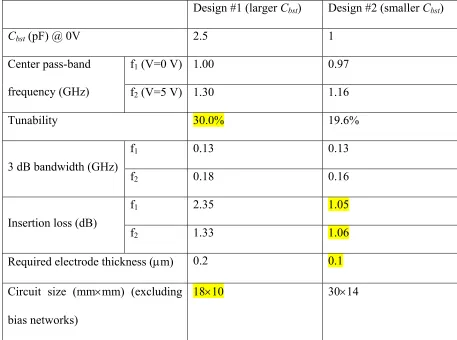
tunability, sharper filter skirt but higher insertion loss.
3.3
Tunable band pass filter design using capacitively loaded resonators
Figure 3.8 (a) a conventional two-pole hairpin filter consisting of two coupled half wavelength resonators (b) hairpin filter with two coupled BST capacitor loaded resonators
A band pass filter can be formed using two or more coupled resonators, as shown in
Figure 3.8 (a). The detailed design procedure can be found in [57][58]. The critical part in the
design is to obtain the optimum coupling coefficient between two resonators to achieve
critical coupled condition. The coupling coefficient is defined as [57][58]:
2 2
2 2
m e
m e
f f
f f K
+ − =
m m
m m
C L LC
LC CL
+ +
= (3.13) Cbst
Cbst
<λ/2
(b) Half wavelength resonators
λ/2