International Journal of Emerging Technology and Advanced Engineering
Website: www.ijetae.com (ISSN 2250-2459,ISO 9001:2008 Certified Journal, Volume 4, Issue 7, July 2014)
655
Case Study on Implementation and Improvement of Timing
Constraints in a 64 bit RISC Processor Using Floor Planning
G.V. Pruthvi Rithvik
1, Sudeep Kumar Dhurua
2, Anusha Daggubatti
3, Priyatham Singirikonda
4 ECE Department , GITAM UNIVERSITY , Visakhapatnam.Abstract—In this paper, the 64- bit RISC processor with 33 instructions is implemented using Verilog HDL and was, in turn , verified on Xillinx ISE simulator. This paper will also present the architecture, of the RISC processor. Total delay and Logical Delay for Data path are also calculated. Floor Planning of 64 bit RISC is also presented , allowing the user to get to know a new design quicker and analyze the consequences of taking different floor planning approaches . The 64-bit processors, on the other hand, can address enormous amount of memory.
Keywords—RISC, Floor Planning , Logic Delay
I. INTRODUCTION
Various suggestions have been made regarding a precise definition of RISC, but the general concept is that of a system that uses a small, highly-optimized set of instructions, rather than a more specialized set of instructions often found in other types of architectures. Another common trait is that RISC systems use the load/store architecture, where memory is normally accessed only through specific instructions, rather than accessed as part of other instructions like add. A common misunderstanding of the phrase "reduced instruction set computer" is the mistaken idea that instructions are simply eliminated, resulting in a smaller set of instructions. In this paper,the Architecture, Data path, are described. The FPGA based RISC Processor has its architecture with BIST, control and timing module is a Hardware module. The ALU is divided into two parts as: The Operational Architecture (OA) and the Testing Architecture (TA). Operational Architecture (OA) does the actual operation of the ALU. It has five units, 4-bit Carry Look Ahead adder (CLA), and a 4-bit AND, OR, XOR and INVERTER gates. An approach of floorplanning to design quicker and its analysis is studied in this paper. If the FPGA targeted is a larger sub 90nm type and the RTL design utilizes a significant amount of FPGA resources, chances are good that the old tool suit can be guided to make a failing design meet timing closure.
In this paper some of the principles applied in floorplanning are explained, and emphasis will be on Xilinx PlanAhead 10.1.
II. WORKING PROCESS
As it is a RISC microprocessor we have a fixed number of instructions which are having the capabilities of performing a maximum level of operations. We have considered 33 instruction sets which will work in this designed microprocessor. The instruction sets are been divided into two parts according to its functions. The functions are handled with the help of two units.
1. Process control units. (PCU)
2. Arithmetic and logical unit. (ALU)
In PCU the instruction which does not need any arithmetic and logical operation will be handled and in
ALU the instruction which strictly need arithmetic and logical operation will be processed.
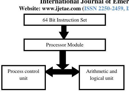
In this microprocessor the main process starts from instruction set. The instruction sets is basically divided into two parts as opcode and operand. But the bit length of the instruction set is 64 bit. Now we are considering first 6 bits as opcode which denotes the specific operation of the 33 instructions and rest of the 58 bits are the raw data which can be the address or can be the operation data. The below diagram describe the bit division in the instruction set.
FIGURE 1: 64 bit Instruction Set
We have decided to make the microprocessor in process flow level and all the processes are been handled by specific process module. The further module is has sub units like PCU and ALU. This sub units are have further specific units which perform the specific operation like Add, Subtract, division and etc.
International Journal of Emerging Technology and Advanced Engineering
Website: www.ijetae.com (ISSN 2250-2459,ISO 9001:2008 Certified Journal, Volume 4, Issue 7, July 2014)
[image:2.612.45.270.110.279.2]656
Figure 1.2: Flow Of Process ControlIn the above figure it is denoted how the process control will flow. The instruction sets will be first handled by the Process control module and then according to the opcode the control will be go to process control unit or the arithmetic and logical unit. The working of each block are been given below
Processor module: It works as a job divider. According to the opcode it will send the control instruction to the specific unit.
Process control unit : This unit handle the instruction which do not need arithmetic and control unit. This unit can handle the operation like.
SKIPZ - Skip the counter if the data entered is zero.
LTR – Load current task register to the source register.
POP- Pop the word out of stack.
PUSH - Push the word into the stack.
Arithmetic and logical unit: This unit is used to perform the arithmetic and logical operation needed for the microprocessor. This unit performs the operation which is denoted by the source register opcode and the result is stored in the destination register. The operations are like
ADD – Arithmetic addition from the source data to the destination data.The Simulation results are shown in Figure.
Figure 1.3:Architechtural Design Of 64 Bit Risc Processor
III. FLOOR PLANNING
Floor planning is the stage of the design where the area of the design is defined. Two regions exist within the design: the core, which contains the cells arranged in rows, and the I/O area, which contains power and ground rings and I/O pins.During the floor planning process the designer can lock parts of the RTL structure or physical parts(e.g. RAM, LUTs or flip flops) in certain FPGA fabric locations. Two structural modules in a design should probably be located adjacent to each other if they are closely attached, i.e. if interconnections are many and timing on the interconnections is critical. In order to enable such an approach the synthesized netlist must describe a structural hierarchy, at least for the RTL structures targeted for floor planning.
64 Bit Instruction Set
Processor Module
Process control unit
[image:2.612.341.550.148.388.2]International Journal of Emerging Technology and Advanced Engineering
Website: www.ijetae.com (ISSN 2250-2459,ISO 9001:2008 Certified Journal, Volume 4, Issue 7, July 2014)
657
Other floor planning attempts focus on I/O interconnections or merging of timing critical parts from one structural module with another structural module. Some floorplans need to be quite elaborate in order to make an FPGA design perform satisfactorily while others can be very rudimentary yet highly effective. The process of establishing a good floorplan is more of a recursive trial and error process loaded with experience and qualified guesses than a well structured linear process.Floorplanning is basically about establishing guide lines for a place and route tool on how to place adesign structure inside an FPGA. Motivations for doing floorplanning can be the desire for: a faster running FPGA design, a design meeting timing closure more consistently or a reduction in tool time. This is done in the following steps for 64 bit RISC processor.
Step 1: First the 64 bit RISC processor source files are re-synthesized in order of the structural hierarchy. This is a necessary step in order to floorplan at a structural level.
Step 2: An analysis of the timing report was conducted and the paths that violate timing constraints were identified. In PlanAhead the timing report from the above run and the accompanying xdl file are loaded. Paths failing to meet timing closure can now be studied in multiple views such as a device view , a design hierarchy view and a schematics view. The views are quite useful for the floorplanning engineer who needs to quickly comprehend the design areas candidating for floorplanning.
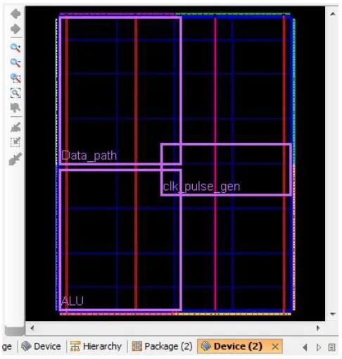
Step 3: A floorplan that makes the new 64 bit processor project meet timing closure should be defined now. Either a floorplan covering only datapath , a floorplan covering ALU and Clk_pulse_gen is verified.These can be selected in different ways as in hierarchical design.Fortunately the XST synthesis tool in ISE 10.1 has introduced a new switch ―-netlist_hierarchy rebuilt‖ that allows a structural hierarchy to be dissolved and then rebuilt after synthesis and logical optimization – from the PlanAhead perspective this switch combines the best from the flattened netlist and the hierarchically netlist.
Step 4: The Processor code is re-synthesized with ―-netlist_hierarchy rebuilt‖ applied and processed using the floorplan in Figure 3.3. The application timing requirements are easily met; actually the new netlist and the floorplan applied can meet request of user.
Step 5: Figure 3.4. This floorplan includes datapath, Clk_pulse_gen and alu, the latter two modules are found right below datapath in hierarchical design.An implementation with the new floorplan results in a new increased clock speed on the timing critical clock network. Comparison to the initial RISC Processor ISE project now reveals a performance gain.In our experiment it is found to be of 9.6 %, which is well.
Later in Plan ahead, by running time ahead with the constraints, ogical delay and Cummulative are found. These results are shown in Table 1.
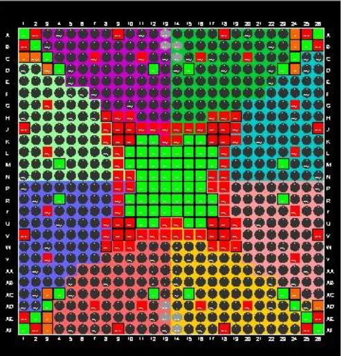
All the pictures shown below are of XC4010XL devices, which is an array of 20 by 20 CLBs. These are represented by small squares. If it is empty, the CLB is not used.Within each CLB, colored squares on the left are F & G function generators, colored squares on the right are the flip-flops, and a colored rectangle in the middle represents the H function generator.
If a square is colored blue, then it is being used.
If a square is colored yellow, then it is a function generator, and the carry logic is active.
If a square is colored magenta, then it is a function generator, and it is being used for single ported RAM.
If a square is colored red, then it is a function generator, and it is being used for dual ported RAM.
If a square is colored green, then it is a function generator, and it is being used for ROM.
If an I/O cell is colored red, then it is being used for a global clock buffer.
An "X" over an I/O cell indicates an I/O cell that is not bonded to a package pin.
An inward pointing arrow on an I/O cell indicates usage as an input..
An outward pointing arrow on an I/O cell indicates usage as an output..
International Journal of Emerging Technology and Advanced Engineering
Website: www.ijetae.com (ISSN 2250-2459,ISO 9001:2008 Certified Journal, Volume 4, Issue 7, July 2014)
658
IV. EXPERIMENTAL RESULTS
FIGURE 2:SIMULATION RESULTS OF 64BIT RISC PROCESSOR
[image:4.612.50.309.152.394.2]Figure 3.1: Package View
[image:4.612.361.528.272.634.2]Figure 3.2:Top View Floor Plan
[image:4.612.50.297.428.685.2]International Journal of Emerging Technology and Advanced Engineering
Website: www.ijetae.com (ISSN 2250-2459,ISO 9001:2008 Certified Journal, Volume 4, Issue 7, July 2014)
[image:5.612.48.293.116.386.2]659
Figure 3.4: Floor Plan Applied For DATA PATH in Step 3 [image:5.612.49.292.410.665.2]FIGURE 3.4: Floor Plan Applied For DATA PATH, ALU, CLK_PULSE_GEN In Step 4 And Step 5
TABLE 1
Showing delay in Data Path of 64 bit RISC Processor
Delay Type Delay Cumulative PBlock
LD 0.633 0.633 ROOT
Net(fo=1) 0.114 0.747 ROOT
OBUF 5.131 5.878 ROOT
Net(fo=0) 0.000 5.878
Total 5.878 5.878
V. CONCLUSION
A 64-bit RISC processor with 33 instruction set has been designed. Every instruction is executed. The design is verified through exhaustive simulations and performing a series of operations with different time intervals and the results has been verified as accurate with the predicted results. RISC processors have been defined explicitly with the aim to apply the available instruction which are describing the basic operation which collectively makes programs to perform massive binary operations.
For filling out, at least parts of the gap growing between FPGA performance and tool suite performance, especially when considering more complex designs for sub 90nm FPGA types ,floorplanning is used . The down side is that some expertise must go along with the floorplanning tool ,starting from scratch, it can take weeks to get acquainted with the tool and finding the floorplan that suite the project requirements.
RISC processor phenomena can also be used in RISC OS designing for Example : ARM RISC OS 5 which can be used in devices powered by ARM9, ARM10, ARM11 and X Scale processors. This RISC architecture can be used in server computing, low power embedded systems and faster DSP’s.
REFERENCES
[1] Samuel O. Aletan, ―An Overview of RISC Architecture,‖Proc.
Symp. Applied Computing, 1992, pp. 11-12.
[2] D. Bhandarkar and D. W. Clark, “Performance from Architecture:
comparing a RISC and a CISC with similar Hardware Organization,‖ Proc. 4th International Conference on Architectural Support for
Programming Languages and Operating Systems, 1991, pp. 310-319.
[3] T. Marshall, ―Worth the RISC,‖ The BYTE, vol. 14, no. 2, 1989, pp.
International Journal of Emerging Technology and Advanced Engineering
Website: www.ijetae.com (ISSN 2250-2459,ISO 9001:2008 Certified Journal, Volume 4, Issue 7, July 2014)
660
[4] R. N. Noyce and M. E. Hoff, ―A History of Microprocessor
Development at Intel,‖ IEEE Micro, vol. 1, no. 1, 1981, pp. 8-21.
[5] J.L. Hennessy, "VLSI Processor Architecture," IEEE Trans.
Computers, vol. C-33, no. 12, Dec. 1984, pp. 1221-1246.573
[6] Aneesh.R and Jiju.K ,―Design of FPGA based 8-bit RISC controller
IP core using VHDL‖, IEEE Micro, vol. 1, no. 7, 2002, pp. 5-19.
[7] Amanjyot Singh Johar ,―16 bit Reduced Instruction Set Computer
(RISC) Processor Design ‖ , IEEE Trans. Computers, vol. A-26, no. 27, Dec. 2007, pp. 113-172.274.
[8] R. Uma ,―Design and Performance Analysis of 8-bit RISC Processor
using Xilinx Tool‖,Adaptive Science & Technology (ICAST), 2012 IEEE 4th International Conference vol., no., pp.78-81, 25-27 Oct. 2012.
[9] Alpesh Kumar Dauda, Nalinikanta Barpanda and Nilamani Bhoi,―