International Journal of Emerging Technology and Advanced Engineering
Website: www.ijetae.com (ISSN 2250-2459,ISO 9001:2008 Certified Journal, Volume 4, Issue 5, May 2014)
425
Self Controllable Pass Transistor Low Power Pulsed Flip-Flop
O.Anjaneyulu
1, A.Veena
2, C.V.Krishna Reddy
31,2KITS, Warangal, Andhra Pradesh, India 3NNRESGI, Hyderabad, Andhra Pradesh, India.
Abstract— In this paper, a novel low power pulsed flip-flop (PFF) using self-controllable pass transistor logic is presented. The pulse generation logic comprising of two transistor AND gate is used in the critical path of the design for improved speed and reduced complexity. In the D to Q path inverter is removed and the transistor is replaced with pass transistor logic. The pass transistor is driven by generated clock pulse is used directly to drive the flip flop output. The presented design is compared with the SCCER and low-power pulse triggered flip-flop with conditional pulse enhancement (LPFF-CE) scheme. As compared to the SCCER, LPFF-CE the proposed pulsed flip-flop (PFF) design features best speed, power. The proposed technique is implemented using TSPICE CMOS 180nm technology. The average power consumption for proposed design is reduced compared with the conventional flip flops.
Keywords— Low power, pulsed flip-flop, pass transistor logic, critical path, self-controllable, power.
I. INTRODUCTION
Flip-flops (FFs) are the basic building blocks of any digital design. In particular, digital designs nowadays often adopt pipelining techniques for high throughput, which increases the use of number of FFs. It is also estimated that in many integrated systems, the power consumption of clock distribution networks and storage elements (FFs and latches), is about 50% of the total system power [1]. In clock system, power is mostly consumed by flip-flops. If the power consumed by the flip-flops is reduced then there will be reduction on total power consumption of the clock system.
Pulse triggered flip-flop (PTFF) is considered as an alternative for the conventional transmission gate (TG) based or master-slave based edge triggered flip-flops [2][3][14]. A PTFF consists of single latch as compared with two latches in the conventional transmission gate (TG).This gives better power performance and speed. A PTFF consists of a latch and pulse generator. If the width of the triggered pulses is narrow then the latch acts like an edge triggered flip-flop [13].
Based on the method of pulse generation employed in the design of pulse-triggered flip-flop, these are of two types: implicit type and explicit type [5]. In an implicit type, the clock-generation is built in logic with latch. In an explicit type, the clock-generation and latch are separate.
Implicit type pulse triggered flip-flop is considered as more power efficient than explicit type pulse triggered flip-flop. This is because, the former merely controls the discharging path while the later generates the pulsetrain.
In this paper, a novel low power implicit type PTFF design featuring self-controllable pass transistor logic is presented. The presented design includes implicit type pulse generation and the use of additional pass transistor driven by the clock pulse to directly drive the output Q.
II. PROPOSED LOW POWER PULSE TRIGGERED FLIP-FLOP
A. Conventional Pulse Triggered Flip-Flop Designs
[image:1.612.336.556.396.587.2]The conventional implicit type pulse triggered flip-flops, which are used as the reference designs for performance comparisons.
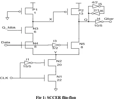
Fig 1: SCCER flip-flop
As shown in Fig. 1[4], shows a refined low power P-FF design named SCCER[11] using a conditional discharged technique [8].In this design, the keeper logic (back-to-back inverters I7 & I8 in ipDCO[15]) is replaced by a weak pull up transistor P1 in conjunction with an inverter I2 to reduce the load capacitance of node X [10]. The discharge path contains nMOS transistors N1, N2, N3, and N4.
International Journal of Emerging Technology and Advanced Engineering
Website: www.ijetae.com (ISSN 2250-2459,ISO 9001:2008 Certified Journal, Volume 4, Issue 5, May 2014)
426 In this design when input data is ―1‖ and node X is discharged through four transistors in series, i.e., N1 through N4, while active with the pull up transistor P1, due to this huge amount of power will be dissipated. In order to control the discharge path powerful pull-down circuitry needed to ensure proper discharging at node X. This gives a longer delay from the delay inverter I1 to widen the discharge pulse width and wider N1&N2 transistors. Fig 2
shows a conditional pulse enhancement based PTFF
(LPFF-CE) [5], which adopts two measures to overcome the problems raised with the existing PTFF designs. The first one is reducing the number of transistors stacked in the discharging path. The other one is a mechanism to support conditional enhancement of the pull down strength when inputdata is high.
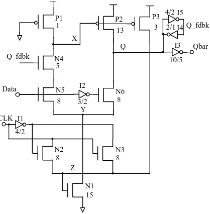
[image:2.612.65.274.315.528.2]N4 P1 N5 N1 N2 N6 P2 8 5 1 4/2 2/1 10/5 8 13 CLK Q_fdbk Q Qbar X I4 I5 I3 Data Y 4/2 I2 3/2 N3 8 8 15 P3 3 Z Q_fdbk I1
Fig 2: Low power pulse triggered flip-flop with conditionally pulse enhancement scheme (LPFF-CPE) [5]
The transistor stacked in discharge path of the SCCER[10] design N2 is removed .Transistor N2 is replaced with a two-input pass transistor logic (PTL) based AND gate to control the discharging of transistor N1.
The present design consists of latch, clock generator, and conditional pulse enhancement scheme .The latch part containing six transistors P1, P2, P3, N4, N5, N6 and an inverter I2.The clock generator containing two N-type pass transistors N2,N3 and an inverter I1.The transistor N1 is called discharging transistor and the P-type pass transistor contribute for pulse enhancement scheme. The two cross coupled inverters I4 and I5 forms keeper logic to hold the output node Q.
B. Proposed Pulsed Flip-Flop Design
The proposed low power pulsed flip-flop using self controllable pass transistor logic scheme is shown in Fig. 3. It consists of latch structure and pulse generation logic. A weak pull-up pMOS transistor P1 with gate connected to ground is pseudo-nMOS logic style used in the first stage of true-single-phase-clocked latch (TSPC) [6]. The load capacitance of node X is reduced. To generate pulse train the pass transistor logic (PTL) based two input AND gate which consists of transistors N2 and N3. A pass transistor N6 driven by the pulse clock is included so that the input data can drive to output node Q directly of the TSPC latch (self-controllable).
The function of this pass transistor is twofold, i.e., driving data to node Q during 0 to 1 transition and discharging node Q during 1 to 0 transitions.
With this, the level of node Q can be quickly pulled up to reduce the data transition delay. This newly employed pass transistor provides a discharging path.
Fig 3: Proposed Low Power Pul.e triggered Flip-Flop
The principle of operation of proposed pulse triggered FF design is explained as follows.
1. FWhen the clock signal is "low", input signal Data is "0", output signal Q is "0‖, and control signal Q_fdbk is "1".
2. When the clock signal is "low", input signal Data is "0 - 1",as the control signal Q_fdbk is "1" at the previous state.
[image:2.612.341.554.364.541.2]International Journal of Emerging Technology and Advanced Engineering
Website: www.ijetae.com (ISSN 2250-2459,ISO 9001:2008 Certified Journal, Volume 4, Issue 5, May 2014)
427 4.When the clock signal is "High-Low", input signal
Data is "1-0", the clock generator is OFF, output signal Q maintains the captured value of the previous state.
5.When the clock signal clock signal is "Low-High", data is "1-0", the clock generator OFF; output signal Q maintains the captured value of the previous state.
III. SIMULATION RESULTS
In order to evaluate the effectiveness of the proposed design is compared with the conventional pulse triggered flip-flops to obtain their performance metrics. These designs include the two implicit type PTFF designs shown in Fig. 1 (SCCER[10]), Fig. 2 (LPFF-CPE [5]). The proposed flip-flop is implemented in 180nm CMOS
technology using TSPICE .The operating temperature 25OC
and VDD=5.0v.
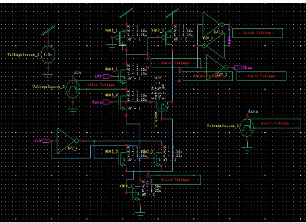
Fig. 4 shows the simulation test bench model. Considering the loading effect of the flip-flop to the previous stage and the clock tree, the power consumption of the clock and data buffer is also included. The output of the flip-flop is loaded with a 20 fF capacitor. An additional capacitance of 3 fF is also placed after the clock buffer. To illustrate the performance of the present work, Fig.10 shows the simulation waveforms of the proposed low leakage LPFF against conventional LPFFs.
Data_In
CLK_In
3fF
20fF Load Qout FF
[image:3.612.339.546.134.307.2]Under Test
Fig 4: Simulation Test bench Model
Fig 5: low power pulse triggered flip flop with conditional pulse enhancement scheme (LPFF-CPE).
Fig 6:low power pulse triggered pulse triggered flip flop with self controllable pass transistor logic
[image:3.612.336.552.341.498.2] [image:3.612.68.269.455.552.2]International Journal of Emerging Technology and Advanced Engineering
Website: www.ijetae.com (ISSN 2250-2459,ISO 9001:2008 Certified Journal, Volume 4, Issue 5, May 2014)
[image:4.612.54.291.138.264.2]428
Table I
Performance Metrics Comparison
We compare the power consumption [14] for 100% switching activity with conventional pulse triggered flip-flop designs.
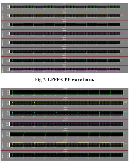
[image:4.612.58.278.366.643.2]Fig.7 shows the simulation waveforms for conventional low power pulse triggered flip-flop with conditional pulse enhancement scheme (LPFF-CPE). Fig. 8 shows the power consumption for 100% data switching activities of proposed flip-flop.
Fig 7: LPFF-CPE wave form.
Fig 8: LPFF with self controllable pass transistor logic
IV. CONCLUSIONS
This paper has proposed a novel low power pulse triggered flip-flop using self controllable pass transistor logic. In this design the no of transistors are reduced. The area for layout is reduced. This design is simulated using 180nm technology and simulation results shows that average power consumption of the proposed design is reduced compared to the conventional designs SCCER, low power pulse triggered flip-flop with conditional pulse enhancement scheme.
REFERENCES
[1] H. Kawaguchi, T. Sakurai, ―A reduced clock-swing flip-flop (RCSFF) for 63% power reduction,‖ IEEE Journal of Solid-State Circuits, vol. 33, no. 5, pp. 807-811, May 1998.
[2] H. Partovi, R. Burd, U. Salim, F.Weber, L. DiGregorio, D. Draper, ―Flow-through latch and edge-triggered flip-flop hybrid elements‖, in IEEE Tech. Dig. ISSCC, pp. 138–139, 1996.
[3] F. Klass, C. Amir, A. Das, K. Aingaran, C. Truong, R.Wang, A. Mehta, R. Heald, and G.Yee, ―A newfamily of semi-dynamic and dynamic flip- flops with embedded logic for high performance processors‖, IEEE Journal of Solid-State Circuits, vol. 34, no. 5, pp. 712–716, May 1999.
[4] J. Tschanz, S. Narendra, Z. Chen, S. Borkar, M. Sachdev, and V. De, ―Comparative delay and energy of single edge-triggered and dual edge- triggered pulsed flip-flops for high performance microprocessors,‖ in Proc. ISPLED, 2001, pp. 207–212.
[5] Yin-Tsung Hwang, Jin-Fa Lin, Ming-Hwa Sheu, ―Low Power Pulse Triggered Flip-Flop Design With Conditional Pulse Enhancement Scheme‖, IEEE Trans. on Very Large Scale Integr. (VLSI).,Vol. 20, No. 2, pp-361-366, Feb. 2012.
[6] Jiren Yuan, Svensson C., ―New TSPC latches and flipflops minimizing delay and power‖, International symposium on VLSI Circuits, pp 160-161, June 1996.
[7] P. Zhao, J. McNeely, W. Kaung, N. Wang, Z. Wang, ―Design of sequential elements for low power clocking system,‖ IEEE Transactions on Very Large Scale Integration (VLSI),Vol. 19, No. 5, pp 914-918, May 2011.
[8] P. Zhao, T. Darwish, M. Bayoumi, ―High performance and low power conditional discharge flip-flop,‖ IEEE Transactions on Very Large Scale Integr. (VLSI) Systems, vol. 12, no. 5, pp. 477–484, May 2004.
[9] B. Kong, S. Kim, Y. Jun, ―Conditional capture flip-flop for statistical power reduction,‖ IEEE J. Solid-State Circuits, vol. 36, no. 8, pp.1263–1271, Aug. 2001.
[10] H. Mahmoodi, V.Tirumalashetty, M. Cooke, and K. Roy, ―Ultra low power clocking scheme using energy recovery and clock gating,‖IEEE Trans. Very Large Scale Integr. (VLSI) Syst., vol. 17, pp. 33–44, Jan. 2009.
International Journal of Emerging Technology and Advanced Engineering
Website: www.ijetae.com (ISSN 2250-2459,ISO 9001:2008 Certified Journal, Volume 4, Issue 5, May 2014)
429
[12] S.H. Rasouli, A. Khademzadeh, A. Afzali-Kusha, and M. Nourani, ―Low power single- and double-edge-triggered flip-flops for high speed applications,‖ Proc. Inst. Electr. Eng.—Circuits Devices Syst., vol. 152,no. 2, pp. 118–122, Apr. 2005.
[13] Y.H. Shu, S. Tenqchen, M.-C. Sun, and W.-S. Feng, ―XNOR-based double-edge-triggered flip-flop for two-phase pipelines,‖ IEEE Trans.Circuits Syst. II, Exp. Briefs, vol. 53, no. 2, pp. 138–142, Feb. 2006.
[14] V. G. Oklobdzija, ―Clocking and clocked storage elements in a multigiga- hertz environment,‖ IBM J. Res. Devel., vol. 47, pp. 567– 584, Sep.2003.