DEVELOPMENT OF AN AC-DC BUCK-BOOST POWER FACTOR CORRECTION
SAHRUDIN BIN SAAD
A project report submitted in partial fulfillment of the requirement for the award of the
Degree of Master of Electrical Engineering
Faculty of Electrical and Electronics Engineering Universiti Tun Hussein Onn Malaysia
ABSTRACT
ABSTRAK
TABLE OF CONTENTS
CHAPTER ITEM PAGE
TITLE
DECLARATION
DEDICATION
ACKNOWLEDGEMENT
ABSTRACT
ABSTRAK
TABLE OF CONTENTS
LIST OF FIGURES
LIST OF TABLES
LIST OF SYMBOLS AND ABBREVIATIONS
i ii iii iv v vi vii
x xii xiii
CHAPTER 1 INTRODUCTION
1.1 Project Overview 1
1.2 Problem Statements 3
1.3 Project Objectives 4
1.4 Project Scopes 4
CHAPTER 2 LITERATURE REVIEW
2.1.1 2.1.2 2.1.2.1 2.1.3 2.1.4 2.1.5 2.1.5.1 2.1.5.2
Introduction of Power Factor
Introduction of Buck-Boost Converter Buck-Boost Converter Formula
Introduction of AC-DC Converter Introduction of PID controller Introduction to switching (Power semiconductor device) MOSFET IGBT 5 6 8 12 13 13 14 15 2.2 2.3
Description of Previous Methods Conclusion
15 19
CHAPTER 3 METHODOLOGY
3.1 Introduction 20
3.2 3.3 3.4 3.5
Power Factor
Buck-boost converter circuit Ac/Dc Switching Power Supply PID controller design
22 23 24 26
CHAPTER 4 RESULTS AND ANALYSIS
4.1 Introduction 28
4.2
4.3
4.4
An Ac-Dc circuit without Power Factor Correction circuit
An Ac-Dc signal open loop Buck Boost Converter
An Ac-Dc Buck Boost Converter by using PID controller (close loop feedback)
29
32
35
CHAPTER 5 CONCLUSION & RECOMMENDATION
5.1 Introduction 38
REFERENCES
APPENDICES
LIST OF FIGURES 1.1 1.2 2.1 2.2 2.3 2.4 2.5 2.6 2.7 3.1 3.2 3.3 3.4 3.5 3.6 3.7 4.1
The Buck Boost PFC Circuit Buck Boost Operation
Phasor Diagram of KW, KVA, KVAr Continuous Mode Buck-Boost Power Stage Waveforms
Buck-Boost converter (a) Basic Circuit (b) Circuit when switch is closed (c) Circuit when switch is opened
Power semiconductor device variety
PFC BBC with Inductor Average Current Controller and PI Controller
Proposed Bridgeless Buck-Boost PFC Converter Prototype Circuit for the Proposed BCM Non-Inverting Buck Boost PFC Converter
Flow chart of planning/procedure for the project Phasor diagram of power factor
The Schematic of a buck–boost converter The buck-boost operation
Input circuit of AC/DC switch power supply
Input equivalent electric circuit of AC/DC switching power supply
An Ac-Dc Buck Boost Converter by using PID controller (close loop feedback
4.3 4.4 4.5 4.6 4.7 4.8 4.9 4.10 4.11 4.12 4.13 4.14 4.15
The voltage output. (without PFC)
The active (P=KW) and reactive power (Q=KVaR). (without PFC)
The power factor. (without PFC)
An Ac-Dc signal open loop Buck Boost Converter The input voltage (250V) and the input current.(open-loop circuit)
The voltage output. (open-loop circuit)
The active (P=KW) and reactive power (Q=KVaR). (open-loop circuit)
The power factor. (open-loop circuit)
An Ac-Dc Buck Boost Converter by using PID controller (close loop feedback)
The input voltage (250V) and the input current.(closed-loop circuit)
The voltage output.(closed-loop circuit)
The active (P=KW) and reactive power (Q=KVaR). (closed-loop circuit)
The power factor.(closed-loop circuit)
LIST OF TABLES
3.1 4.1
4.2
4.3
PID parameter
Power factors of circuit without PFC circuits under different loads.
Power factors of Ac-Dc signal open loop Buck Boost Converter
Power factors of Ac-Dc Buck Boost Converter by using PID controller (close loop feedback)
26 31
34
LIST OF SYMBOLS AND ABBREVIATIONS ac dc PFC PID Kp Ki Kd EMI S1 L D C Vin Vout kW kVA kVar P Q pf v D CCM DCM MOSFET Alternating current Direct current
Power Factor Correction Proportional-integral-derivative Proportional gain Integral gain Derivative gain Electromagnetic Interference Switch 1 Inductant Diode Capacitor Voltage input Voltage output Useful power Total power Magnetic power Active power Reactive power Power factor Voltage Duty cycle
Continuous current mode Discontinuous current mode
IGBT IACMC BBC BCM THD
Insulated Gate Bipolar Transistor
Inductor Average Current Mode Control Buck-Boost Converter
CHAPTER 1
INTRODUCTION
1.1Project Overview
In the last years, the number and power level of power electronic converters in both industrial and household applications have been significantly increased. In many cases, these applications perform ac to dc conversion, whose classical solutions uses simple diode bridge rectifiers and large dc link capacitors. According to Vitor (2001), such rectifiers produce a large amount of harmonics in the input currents, leading to harmonic distortion and causing poor input effective power factor and source voltage disturbances. Switching the power supplies is widely used to reduce the input-current harmonic distortion. Buck, boost, and buck boost are the three basic switching power supply topologies in common use.
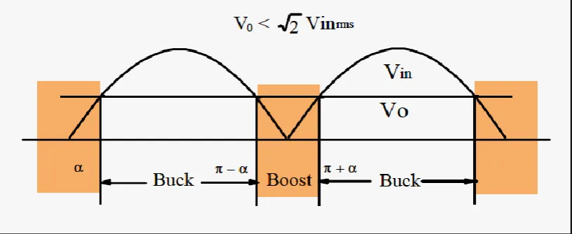
According Everett Rogers, 1999, the buck-boost is a popular nonisolated, inverting power stage topology. The buck-boost converter is commonly applied to Power Factor Corrections applications and it is one type of AC-DC converter which is either for step up or step up-step down respectively. Therefore, it is sometimes called as a step-up/down power stage. Power supply designers choose the buck-boost power stage because the output voltage is inverted from the input voltage, and the output voltage can be either higher or lower than the input voltage. Figure 1.1 shows the Buck-Boost PFC Circuit while Figure 1.2 shows the Buck Boost operation.
Figure 1.1: The Buck Boost PFC Circuit
[image:13.595.115.527.282.453.2] [image:13.595.116.526.542.709.2]With the increasing demand for power from the ac line and more stringent limits for power quality, power factor correction has gained great attention in recent years. A variety of circuit topologies and control methods have been developed for the PFC application. One of the biggest problems in power quality aspects is the harmonic contents in the electrical system. Most of the current harmonics are due to the nonlinear operation of the power converters and are furnaces.
By applying a correct power factor correction (PFC), the power consumption is reduced to improve energy efficiency. Reduced power consumption means less greenhouse gas emissions and fossil fuel depletion by power stations. Reduction of electricity bills, reduction of power losses in transformers and distribution equipment are also the benefits of applying the correct PFC. Besides, the equipment life are extended due to the lessen of the electrical burden on cables and electrical components. With the problems occurred and the benefits gained by reason of the power factor correction, an ac-dc buck-boost power factor correction is proposed in this project.
1.3Objectives of Project
This project has been developed to enhance the achievement in the following matters:
a) To develop modelling of AC-DC Buck-Boost Converter.
1.4Scope Of Project
CHAPTER 2
LITERATURE REVIEW
2.1Theories
Theories are important in projects that need to be developed. A theory presents a systematic way understanding events, behaviours and/or situations. A theory is a set of interrelated concepts, definitions, and propositions that explained or predicts events or situations by specifying relations among variables. (Glanz K et al, 2008). There are combinations of theories used in this project. They are theories of Power Factor, Buck Boost Converter, and AC-DC Converter.
2.1.1 Introduction of Power Factor
a) Power factor (pf) = Useful power (kW) divided by the total power
(kVA),
b) Power factor (pf) = The cosine of the angle between useful power and
[image:17.595.116.529.217.318.2]total power = cos ø.
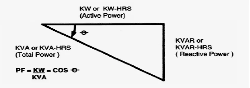
Figure 2.1 below shows the phaser diagram of kW, kVAr and kVAr.
Figure 2.1 : Phasor Diagram of KW, KVA, KVAr
The phasor diagram above can be translated to the formula as below.
𝑷. 𝑭 =𝒖𝒔𝒆𝒇𝒖𝒍 𝒑𝒐𝒘𝒆𝒓(𝒌𝒘)
𝒕𝒐𝒕𝒂𝒍 𝒑𝒐𝒘𝒆𝒓 (𝒌𝑽𝑨)
= 𝒑
𝑽𝒓𝒎𝒔 𝒙 𝑰𝒓𝒎𝒔
2.1.2 Introduction of Buck Boost Converter
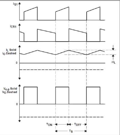
of one complete switching cycle, Ts. The duration of the OFF state is called TOFF. Since there are only two states per switching cycle for continuous conduction mode, TOFF is equal to (1−D) × TS. The quantity (1−D) is sometimes
called D’. These times are shown along with the waveforms in figure 2.2.
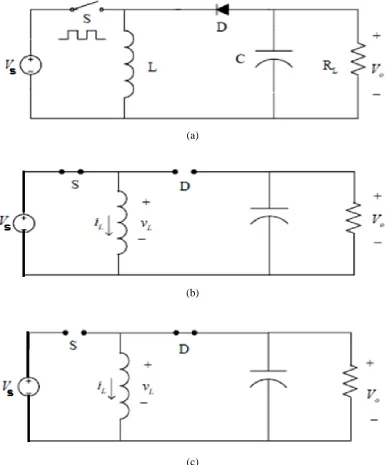
[image:18.595.116.517.214.664.2]2.1.2.1Buck-Boost Converter Formula
The equivalent circuit for buck-boost converter in two switching modes; closed and opened is shown in figure 2.3.
(a)
(b)
(c)
[image:19.595.123.513.168.634.2](2.1)
(2.2)
The rate of change for the inductor current is a linearly constant, so equation 2.2 can be expressed as
(2.3)
Buck-boost analysis when the switch is opened;
(2.4)
(2.5)
The rate of change for inductor current is constant, thus the change in current at opened circuit is
(2.6)
Solving for Vout
(2.7)
Equation 2.7 shows the output voltage produced using buck-boost converter method has an opposite polarity compared to input voltage. These converter can produced three stage of voltage depend on the duty cycle;
i. If the duty cycle is greater than 0.5 (D > 0.5), the output voltage will be higher than the input voltage (boost mode).
ii. If the duty cycle is equal to 0.5 (D = 0.5), the output will produce the same amount of voltage as input voltage.
iii. If the duty cycle is lower than 0.5 (D < 0.5), the output voltage will be lower than the input voltage (buck mode).
In the buck-boost converter, the source is never connected directly to the load. Energy is stored in the inductor when the switch is closed and transferred to the load when the switch is opened. Hence, the buck boost converter is also referred to as an indirect converter.
Assuming no power losses in the converter, power absorbed by the load must be equal with power supplied by the source,
Average source current is related to average inductor current as;
(2.10)
Thus, equation 2.9 can be written as;
(2.11)
Solving for IL
(2.12)
For continuous current mode IL must be greater than Maximum and minimum inductor current;
(2.13)
(2.14)
For continuous current, the inductor current must remain positive. Therefore, in order to determine the boundary between continuous (CCM) and discontinuous current (DCM), Imin in equation 2.14 is set to zero.
(2.15)
The output voltage ripple for the buck boost converter;
(2.16)
Solving for
(2.17)
Thus
(2.18)
2.1.3 Introduction of AC-DC Converter
Proportional-integral-derivative (PID) control: Over 90% of the controllers in operation today are PID controllers (or at least some form of PID controller like a P or PI controller). This approach is often viewed as simple, reliable, and easy to understand.
Typical steps for designing a PID controller are;
i. Determine what characteristics of the system need to be improved ii. Use KP to decrease the rise time.
iii. Use KD to reduce the overshoot and settling time. iv. Use KI to eliminate the steady-state error.
Conventional PID controllers have been extensively used in industry, due to their effectiveness for linear systems, ease of design and inexpensive cost. Despite their effectiveness for linear systems, conventional PID controllers are not suitable for nonlinear systems and higher-ordered and time-delayed systems, not to mention complex and vague systems that require expert knowledge. For these reasons, it is worth developing fuzzy-logic-based controllers which have the capability to handle not only linear, as well as indistinct defined systems.
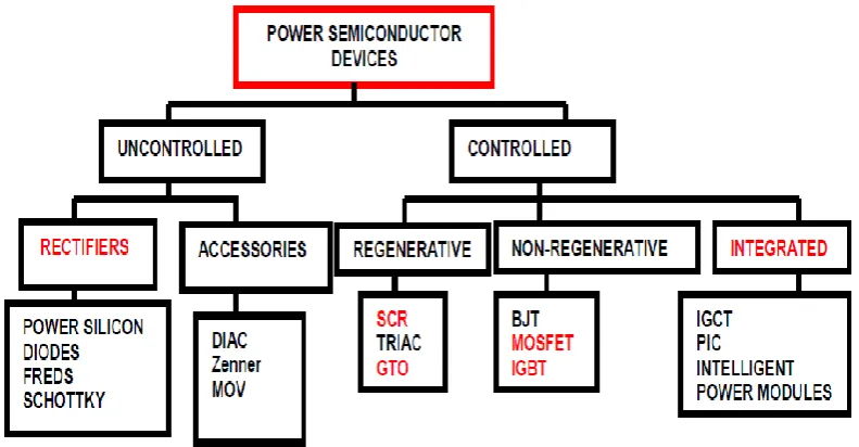
2.1.5 Introduction to switching (Power semiconductor device)
The range of power devices developed over the last few decades can be
represented as a in figure 2.4 on the basis of their controllability and other dominant
Figure 2.4: Power semiconductor device variety
In designing buck-boost converter, converter with non-regenerative power semiconductor compenent is selected to be a switching device. Most of buck-boost converter designed only used either mosfet or igbt nowadays.
2.1.5.1MOSFET (Metal Oxide Semiconductor Field Effect Transistor)
[image:25.595.119.515.78.284.2]It is a voltage controlled four-layer device with the advantages of the MOSFET driver and the Bipolar Main terminal. The switching times can be controlled by suitably shaping the drive signal. This gives the IGBT a number of advantages: it does not require protective circuits, it can be connected in parallel without difficulty, and series connection is possible without snubbers. The IGBT is presently one of the most popular devices in view of its wide ratings, switching speed of about 100 KHz, an easy voltage drive and a square safe operating area devoid of a second breakdown region.
2.2 Description of Previous Case Study
At this section, three previous case studies are described. The case studies are “Inductor Average Current Mode Control For Single Phase Power Factor Correction Buck Boost Converter”, “A Novel Bridgeless Buck Boost PFC Converter” and “Non-inverting Buck-Boost Power Factor Correction Converter with Wide Input-Voltage-Range Applications”.
2.2.1 Inductor Average Current Mode Control For Single Phase Power
Factor Correction Buck Boost Converter
implemented at outer loop, which produce the excellence performance of output voltage regulation for BBC under different conditions.
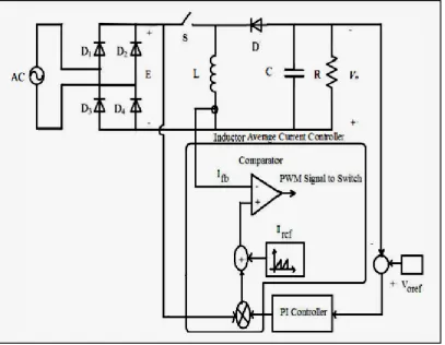
The PI controller is developed by using state space average model of BBC. The single phase PFC BBC with proposed controllers is shown in Figure 2.5 below. In this paper, Matlab/Simulink is used to do the simulation of the proposed system with its control. The simulation results show a nearly unity power factor can be attained and there is almost no change in power factor when the line frequency is at various ranges. The writers made a conclusion that IACMC is advantageous compared to peak current mode controller in the application when the line frequency is changing largely. Besides, the proposed technique offers definite befits over the conventional boost converter and it is easy to understand, is easy to implement, and draws sinusoidal input current from AC source for any DC output voltage condition. They suggested that, the hardware should be developed in the future, to study further about the PFC BBC with proposed controlled.
[image:27.595.117.525.409.725.2]This paper was written in 2007 and the writers of this paper are Wang Wei, Liu Hongpeng, Jiang Shigong and Xu Dianguo from the Harbin Institute of Technology, China. A novel bridgeless buck-boost PFC topology is proposed in this paper. This proposal is to resolve the problem of Conventional Cascade buck-boost PFC (CBB-PFC) converter suffers from the high conduction loss in the input rectifier bridge. The proposed PFC converter (as shown in Figure 2.6) which removes the input rectifier bridge has three conduction semiconductors at every moment. The proposed topology reduces the conduction semiconductors, reduces conduction losses effectively, and improves the efficiency of converter compared to CBB-PFC topology.
[image:28.595.120.522.575.742.2]This is because CBB-PFC converter consists of bridge rectifier and buck boost converter, and has four conduction semiconductors at every moment. Thus, with the increase of power rating, the conduction loss of converter will increase rapidly. The novel bridgeless buck boost PFC topology is also suitable for use in the wide input voltage range. In this paper, the average current mode control was implemented with UC3854, the theoretical analysis and design of detection circuits was presented. They built an experimental prototype with 400V/600W output and line input voltage range from 220VAC to 380VAC. The experimental results show that the proposed converter can improve 0.8% efficiency comparing CBB-PFC converter.
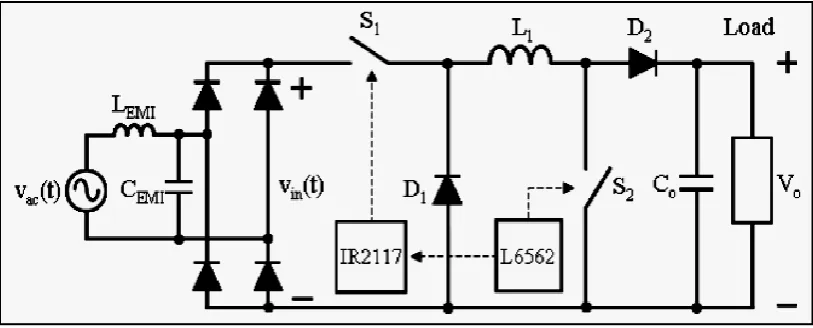
2.2.3 Non-inverting Buck-Boost Power Factor Correction Converter with
Wide Input-Voltage-Range Applications
Written by Ray-Lee and Rui-Che Wang in 2009, this paper presents a non-inverting buck-boost based power-factor correction (PFC) converter operating in the boundary-conduction-mode (BCM) for the wide input-voltage-range applications. Unlike other conventional PFC converters, the proposed non-inverting buck-boost based PFC converter has both step-up and step-down conversion functionalities to provide positive DC output-voltage. It is the combination of a buck converter and a converter has both step-up and step-down conversion functionalities to provide positive DC output-voltage. It is the combination of a buck converter and a boost converter. This converter operates in the buck or boost mode, which is dependent on the level of the instantaneous input voltage Vin(t). When the level of the instantaneous input voltage Vin(t) is higher than the DC output voltage V0, the converter operates in the buck mode; otherwise the converter operates in the boost mode. However, the BCM non-inverting buck-boost PFC converter with the buck boost mode cannot be used to achieve high power factor, which is caused by the constant on-time of BCM. There is increment of the inductor-current during the on time in the buck and boost mode and the instantaneous values of the incremental are different. Therefore, these differences at the transitions between the modes cause the distortion on the inductor current. In order to reduce the turn-on switching-loss in high frequency applications, the BCM current control is employed to achieve zero current turn-on for the power switches. It is operated in the buck-boost mode to eliminate the distorted inductor current.
high-0.99; the THD is 8% and the efficiency is 90% while with the high input line-voltage (264Vrms) the PF is 0.98; the THD is 14% and the efficiency is 91%.
Figure 2.7: Prototype Circuit for the Proposed BCM Non-Inverting Buck Boost PFC Converter
2.3 Conclusion
CHAPTER 3
METHODOLOGY
3.1 Introduction
The focus of this chapter is to provide further details of methodology and approaches to completing this research. This chapter discusses on three main parts, which is designing An Ac-Dc circuit without Power Factor Correction (PFC) circuit, An Ac-Dc signal open loop Buck Boost Converter and An Ac-Dc Buck Boost Converter by using PID controller (close loop feedback). MATLAB R2009b simulink is use to achieve the objective of the research.
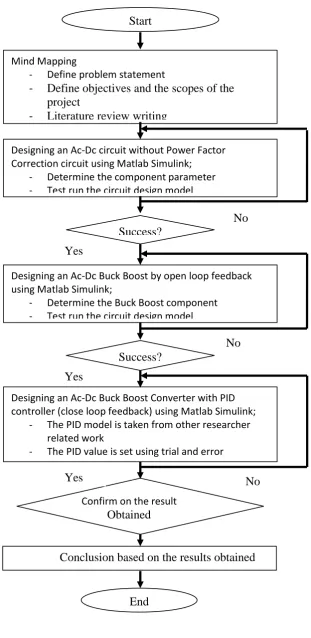
Figure 3.1: Flow chart of planning/procedure for the project Mind Mapping
- Define problem statement
- Define objectives and the scopes of the project
- Literature review writing
- Finalized concepts and methodology Designing an Ac-Dc circuit without Power Factor Correction circuit using Matlab Simulink;
- Determine the component parameter - Test run the circuit design model
Success?
Designing an Ac-Dc Buck Boost by open loop feedback using Matlab Simulink;
- Determine the Buck Boost component - Test run the circuit design model
Success?
Designing an Ac-Dc Buck Boost Converter with PID controller (close loop feedback) using Matlab Simulink;
- The PID model is taken from other researcher related work
- The PID value is set using trial and error
Confirm on the result Obtained
Conclusion based on the results obtained
3.2 Power Factor
In most modern electrical distribution systems, the predominant loads are resistive and inductive. Resistive loads are incandescent lighting and resistance heating. Inductive loads are A.C. Motors, induction furnaces, transformers and ballast -type lighting. Inductive loads require two kinds of power: (1) active (or working) power to perform the work (motion) and (2) reactive power to create and maintain electro-magnetic fields. The vector sum of the active power and reactive power make up the total (or apparent) power used. This is the power generated by the utility for the user to perform a given amount of work.
Active power is measured in KW (1000 Watts)
Reactive power is measured in kVAR (1000 Volt-Amperes Reactive)
Total Power is measured in KVA (1000 Volt-Amperes)
[image:33.595.119.521.448.590.2]Power factor then is the ratio of active power to total power. We can illustrate these relationships by means of a right triangle. (See Figure 3.2)
Figure 3.2: Phasor diagram of power factor
3.3 Buck-boost converter circuit
Figure 3.3: The Schematic of a buck–boost converter
The buck–boost converter is a type of DC-to-DC converter that has an output voltage magnitude that is either greater than or less than the input voltage magnitude. Two different topologies are called buck–boost converter. Both of them can produce a range of output voltages, from an output voltage much larger (in absolute magnitude) than the input voltage, down to almost zero.
The inverting topology:
(if, for example, the supply is a battery) as the supply and diode polarity can simply be reversed. The switch can be on either the ground side or the supply side.
Principle of operation:
The basic principle of the buck–boost converter is fairly simple (see figure 3.4):
1) While in the On-state, the input voltage source is directly connected to the inductor (L). This results in accumulating energy in L. In this stage, the capacitor supplies energy to the output load.
[image:35.595.119.521.359.603.2]2) While in the Off-state, the inductor is connected to the output load and capacitor, so energy is transferred from L to C and R.
Figure 3.4: The buck-boost operation
3.4Ac/Dc Switching Power Supply
REFERENCES
Beams, D. and Boppana, S. (2010). “Modelling and Simulation of Off-Line Boost Power Factor Correction Circuits.” USA : University Of Texas at Tyler.
Choi, B., Hong, S., and Park, H. (2000) “Modeling and small- signal analysis of controlled on-time boost power factor correction circuit.” Proceedings of the Third International Power Electronics and Motion Control Conference, pp. 490-495.
Everett Rogers. (1999). “Understanding Buck-Boost Stages in Switchmode Power Supplies.”SLVA059.pp 1-32.
Glanz K, Rimer BK, Viswanath K. (2008). “Health Behavior and Health Education: Theory, Research, and Practice (4th ed). San Francisco: Jossey-Bass.
Jayahar, D. And Dr, Ranihemamalini, R. (2011). “Inductor Average Current Mode Control For Single Phase Power Factor Correction Buck Boost Converter.” Chennai, India: St. Peters Engineering College.
John Ware. (2006). “Power Factor Correction.”IEE Wiring Matters.pp 22-24.
Mahmoud Shaker, A, Ass. Prof. Dr. M. Salleh, A. and Prof. Dr. S. Ismail, Kais (2008). “Design and Simulation of Power Factor Correction for AC/DC Converter.” Iraq :Baghdad and Al Nahrin University.
Moschopoulos, G. and Zheng, Y. (2006). “Buck-Boost Type AC/DC Single Stage Converter.” London, Ontaria, Canada: University of Western Ontario.
Muhammad H. Rashid, (2004): Power Electronics Circuits, Devices, and Applications’’ Electrical computer Engineering University of west Florida.
Ping, L., Yu, M., Yong, K., Hui, Z., and Jian, C.(1999), “Analysis of single-phase boost power-factor correction (PFC) converter.” Hong Kong : Proceedings of the 1999 IEEE International Conference on Power Electronics and Drive Systems.
Ray Lee, Lin. and Rui Che, Wang. (2010). “Non-inverting Buck-Boost Power Factor Correction Converter with Wide Input Voltage Range Applications.” Tainan City, Taiwan :National Cheng Kung University.
Robert W. Erickson, “DC-DC Power Converters” Wiley Encyclopedia of Electrical and Electronics Engineering, 2007.
Tahami, F., Gholami, B., and Amadhian, H., (ISIE 2008) “Modeling of the boost power-factor correction rectifier in mixed conduction mode using PWA approximation.” Proceedings of the 2008 IEEE International Symposium on Industrial Electronics, pp. 254-258.
Vitor Fernao Pires and Jose Fernando A. Silva (2001). “Single Stage Three-Phas Buck-Boost Type AC/DC Converter With High Power Factor.” Portugal: Centro University Tecnica de Lisboa..