~
c:
I
RESEARCH, INC.
CRAY X_Mp™
COMPUTER SYSTEMS
FOUR-PROCESSOR
MAINFRAME REFERENCE MANUAL
·~
__ Ii=::ai""
...."
RECORD OF REVISION RESEARCH. INC. PUBLICATION NUMBER HR-0097
Each time this manual is revised and reprinted. all changes issued against the previous version are incorporated into the new version and the new version is assigned an alphabetic level.
Every page changed by a reprint with revision has the revision level in the lower righthand corner. Changes to part of a page are noted by a change bar in the margin directly opposite the change. A change bar in the margin opposite the paQe number indicates that the entire page is new. If the manual is rewritten. the revision level changes but the manual does not contain change bars.
Requests for copies of Cray Research. Inc. publications should be directed to the Distribution Center and comments about these publications should be directed to:
CRAY RESEARCH. INC. 2520 Pilot Knob Road Suite 310
Mendota Heights. Minnesota 55120
Revision
A
B
Description
August 1984 - Original printing.
November 1985 - Reprint with revision.
Memory addressing
format changes for 64K-chip systems and 16-million-word
memories were added.
Numerous editorial changes and
corrections were also added.
This revision obsoletes all
previous printings.
August 1986 - Reprint with revision.
Corrections were made to
the SECDED maintenance mode function statement documentation
and the underflow detection statement.
Additions were made to
the scalar reference hold issue condition and the vector load
information.
The clock period (CP) time on serial number 213
and above has been upgraded from 9.5-ns to 8.5-ns.
Additional
information about the new CRAY X-MP/44 computer system was
added.
Numerous technical and editorial changes and
corrections were also made.
This revision obsoletes all
previous printings.
PREFACE
This manual describes the functions of CRAY X-MP four-processor computer systems. It is written to assist programmers and engineers and assumes a familiarity with digital computers.
This manual describes the overall computer system, its configurations, and equipment. It also describes the operation of the Central Processing Units (CPUs) that execute instructions, provide memory protection, report hardware exceptions, and provide interprocessor communications within the system.
The following publications give details of the I/O Subsystem (lOS), the disk storage units (DSUs), and the Solid-state Storage Device (SSD):
HR-0030 HR-0031 HR-0630 HR-0077
I/O Subsystem Hardware Reference Manual
SSD Solid-state Storage Device Hardware Reference Manual Mass Storage Subsystem Hardware Reference Manual
Disk Systems Hardware Reference Manual
/ / / / / / / / / / / / / / / / / / / / / / / / / / / / / / / / / / / / / / / / / / / / / / / / / / / / / / /
WARNING
This equipment generates, uses, and can radiate radio frequency energy and if not installed and used in accordance with the instructions manual, may cause interference to radio communications. It has been tested and found to comply with the limits for a
Class A computing device pursuant to Subpart J of Part 15 of FCC Rules, which are designed to provide
reasonable protection against such interference when operated in a commercial environment. Operation of this equipment in a residential area is likely to cause interference, in which case, the user at his own
expense will be required to take whatever measures may be required to correct the interference.
CONTENTS
PREFACE • • • • • . • • • • • . • • • • • • • • • . • . • . . • • • i i i
1.
2.
SYSTEM DESCRIPTION •
CONVENTIONS Italics
Register conventions • . • • • Number conventions • • • • • •
Clock period . • • . • • • • • SYSTEM COMPONENTS . • . . • • • •
Central Processing Units
Interfaces • • . • . • • • • • • • • • •
1/0 Subsystem • • • • • Disk storage units
Solid-state Storage Device Condensing units • . . . Power distribution units
Motor-generator units . . • • SYSTEM CONFIGURATION • . . .
CPU RESOURCES CENTRAL MEMORY
Memory organization
Memory addressing . . • • •
·
·
·
·
·
·
·
·
·
·
·
· · · ·
· · ·
·
· · · ·
·
·
·
·
· ·
· · ·
·
· ·
·
·
·
· ·
· ·
·
·
· ·
· ·
· · ·
·
· ·
·
·
· ·
Memory addressing for 32-bank, 64K-chip,
4-million-·
·
·
·
·
·
·
·
·
·
·
·
·
·
word system • . . . . • • . . • . • . . . • • Memory addressing for 64-bank, 16K-Chip, 8-million-word system • . . • . . • . . • . . . • • . Memory addressing for 32-bank, 64K-chip, 8-million-word system • . • • . • • . • • • • . • • . • • • Memory addressing for 64-bank, 64K-chip,
16-million-word system • . . . . • • .
Memory access • • . .
Conflict resolution . • Bank Busy conflict •
Simultaneous Bank conflict Section Access conflict Memory access priorities
2. CPU RESOURCES (continued)
3.
INTER-CPU COMMUNICATION SECTION Real-time clock
Inter-CPU communication and control
Shared Address and Shared Scalar registers Semaphore registers • • • • • • • • . . . Shared register and semaphore conflicts . CPU INPUT/OUTPUT SECTION . • • • • • • • • • • . . Data transfer for Solid-state Storage Device .
Data transfer for I/O Subsystem . . . • • • 6 Mbyte per second channels • • • • • • • • Multi-CPU programming • • • • • • • • • • • 6 Mbyte per second channel operation . • • • • . Input channel programming • . • . • . • • •
Input channel error conditions . • • . • • • • • . Output channel programming • • • • • • • • • Programmed Master Clear to external device . • • • • • Access to Central Memory . . • . • • • • • • • • . I/O lockout • . . . . • • • • • . Memory bank conflicts . . • • •
I/O memory conflicts . . I/O memory request conditions I/O memory addressing • . • .
CPU CONTROL SECTION
INSTRUCTION ISSUE AND CONTROL Program Address register •
Next Instruction Parcel register • • Current Instruction Parcel register Lower Instruction Parcel register Instruction buffers . . . • • . EXCHANGE MECHANISM . . . . •
Exchange Package • . . Processor number
Memory error data . . . • . Program Address register Memory field registers
Mode register • . • • • • • . Vector not used (VNU) • • •
Enable Second Vector Logical (ESVL) • Flag register . . . . • • . • • •
Exchange Address register . • • . . • • . Enhanced Addressing Mode (EAM) • . . . Data Base Address register
Program State register
Cluster Number register • . . • . . . Data Limit Address register • •
3. CPU CONTROL SECTION (continued)
4.
Active Exchange Package • • . • • • • • . Exchange sequence • • • • • . • • • Exchange initiated by deadstart sequence Exchange initiated by Interrupt flag set Exchange initiated by program exit
Exchange sequence issue conditions
Exchange Package management • . . . . • • • MEMORY FIELD PROTECTION • . • •
Instruction Base Address register Instruction Limit Address register . Data Base Address register •
Data Limit Address register Program range error
Operand range error PROGRAMMABLE CLOCK • .
Instructions . • . .
Interrupt Interval register
Interrupt Countdown counter • • • • • . Clear programmable clock interrupt request •
PERFORMANCE MONITOR . . • .
DEADSTART SEQUENCE • .
CPU COMPUTATION SECTION
OPERATING REGISTERS ADDRESS REGISTERS
A registers
B registers . • • . • . • . SCALAR REGISTERS •
S registers
T registers . • • . VECTOR REGISTERS .
V registers
V register reservations and chaining Vector control registers • • •
Vector Length register . • • . Vector Mask register • • • • FUNCTIONAL UNITS . • • . • . • • .
Address functional units . • .
Address Add functional unit . Address Multiply functional unit Scalar functional units . • • . •
Scalar Add functional unit • . . . Scalar Shift functional unit
Scalar Logical functional unit
Scalar Population/Parity/Leading Zero functional unit
4. FUNCTIONAL UNITS (continued)
Vector functional units • • • . • • • • • . • • • .
Vector functional unit reservation • • • • • • • • . Vector Add functional unit • • • • • • • . Vector Shift functional unit
Vector Logical functional units . . . . • • . . Vector Population/Parity functional unit
Floating-point functional units • . . • Floating-point Add functional unit
Floating-point Multiply functional unit. Reciprocal Approximation functional unit ARITHMETIC OPERATIONS • • • •
Integer arithmetic . . • • . . . • . Floating-point arithmetic . . . • •
Normalized floating-point numbers Floating-point range errors . . .
Floating-point Add functional unit . Floating-point Multiply functional unit Floating-point Reciprocal Approximation functional unit
Double-precision numbers Addition algorithm . • • . Multiplication algorithm Division algorithm
Newton's method
Derivation of the division algorithm LOGICAL OPERATIONS . . . . • . . . . • . . • •
5. CPU INSTRUCTIONS INSTRUCTION FORMAT
1-parcel instruction format with discrete
j
andk
fields . 1-parcel instruction format with combinedj
and k fields .2-parcel instruction format with combined j, k,
and m fields . . • . • • • • • . . . • •
2-parcel instruction format with combined i, j,
k,
and
m
fields . • . . . • • . SPECIAL REGISTER VALUES . . • • . INSTRUCTION ISSUE • . • . . • . . INSTRUCTION DESCRIPTIONSAPPENDIX SECTION
A. INSTRUCTION SUMMARY FOR CRAY X-MP FOUR-PROCESSOR COMPUTER SYSTEMS
B.
C.
D.
6 MBYTE PER SECOND CHANNEL DESCRIPTIONS
6 MBYTE PER SECOND INPUT CHANNEL SIGNAL SEQUENCE Data bits 20 through 2 15 •
Parity bits 0 through 3
Ready signal • • • • Resume signal . • • • . • Disconnect signal
6 MBYTE PER SECOND OUTPUT CHANNEL SIGNAL SEQUENCE Data bits 2 0 through 2 15 • • • • • • • • • Parity bits 0 through 3 • • • •
Ready signal . • • Resume signal Disconnect signal
PERFORMANCE MONITOR
SELECTING PERFORMANCE EVENTS READING PERFORMANCE RESULTS TESTING PERFORMANCE COUNTERS •
SECDED MAINTENANCE FUNCTIONS' • • . .
VERIFICATION OF CHECK BIT STORAGE VERIFICATION OF CHECK BIT GENERATION .
VERIFICATION OF ERROR DETECTION AND CORRECTION • CLEARING MAINTENANCE MODE FUNCTIONS
FIGURES 1-1 1-2 1-3 1-4 1-5 1-6 1-7 1-8 1-9 1-10 1-11 2-1 2-2
CRAY X-MP Model 48 Mainframe with a Cray IIO Subsystem and a Solid-state Storage Device • . • • . • •
Basic Organization of the Four-processor System Control and Datapaths for a Single CPU
Typical Interface Cabinet . • • • •
IIO Subsystem Chassis • • • • . • . Solid-state Storage Device Chassis Condensing Unit . • . . •
Power Distribution Units . • . . . Motor-generator Equipment . . . . .
Block Diagram of a Typical Four-processor System with Full Disk Capacity . . . . • . • . . . . Block Diagram of a Typical Four-processor System with Block Multiplexer Channels . . . • • . . Central Memory Organization for a Four-processor System . Memory Datapath with SECDED
FIGURES (continued) 2-5 2-6 2-7 3-1 3-2 3-3 3-4 4-1 4-2 4-3 4-4 4-5 4-6 4-7 4-8 4-9 4-10 4-11 5-1 5-2 5-3 5-4 5-5 5-6 5-7 5-8 5-9 5-10 5-11 5-12 TABLES 1-1 2-1 2-2 5-1 B-1 B-2 C-1 INDEX
Basic I/O Program Flowchart • • • • • Channel I/O Control . • • • •
Input/Output Data Paths • .
Instruction Issue and Control Elements Instruction Buffers . . • • . • • • •
Exchange Package for a Four-processor System Read Address (CSB) Bits (64 Banks) • • • .
Address Registers and Functional Units . . . • . . Scalar Registers and Functional Units . • • • . . • • . Vector Registers and Functional Units . • • • • • • • • . Integer Data Formats • • . . . . • . . . • • . Floating-point Data Format . • . . . • • • .
Internal Representation of Floating-point Number (Octal) Exponent Matrix for Floating-point Multiply Unit • . • • Integer Multiply in Floating-point Multiply Functional Unit . 49-bit Floating-point Addition . . • . • • • • • • • . • • . Floating-point Multiply Partial-product Sums Pyramid . • . . Newton's Method . . • • • . . • . • . . • • • • .
General Form for Instructions • . • . • . • . . 1-parcel Instruction Format with Discrete j and k Fields
1-parcel Instruction Format with Combined
j
andk
Fields 2-parcel Instruction Format with Combined j,k,
and m Fields 2-parcel Instruction Format for a Branch with Combined i,j,
k, and m Fields . • • . . • . . • • • . • • . • . . . . • . . 2-parcel Instruction Format for a 24-bit Immediate Constant with Combined i, j,k,
and m Fields • • • • . • . . • • • • . Vector Left Double Shift, First Element, VL Greater than 1 Vector Left Double Shift, Second Element, VL Greater than 2 . Vector Left Double Shift, Last Element • • • .Vector Right Double Shift, First Element Vector Right Double Shift, Second Element, VL Greater than 1 . • • . . • . . . • Vector Right Double Shift, Last Operation •
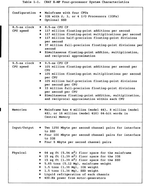
CRAY X-MP Four-processor System Characteristics • Memory Addressing Formats . . • •
Channel Word Assembly/Disassembly Special Register Values • • . . . Input Channel Signal Exchange • . Output Channel Signal Exchange
Performance Counter Group Descriptions
SYSTEM DESCRIPTION
1
CRAY X-MP four-processor computer systems are powerful, general purpose machines that contain four central processing units (CPUs). Like all CRAY X-MP multiprocessor systems, they are able to achieve extremely high multiprocessing rates by efficiently using the scalar and vector
capabilities of all CPUs combined with the systems' solid-state, random-access memory (RAM) and shared registers.
Vector processing is the performance of iterative operations on sets of ordered data. When two or more vector operations are chained together, two or more operations can be executing simultaneously; therefore, the computational rate for vector processing greatly exceed the computational rates of conventional scalar processing. Scalar operations complement the vector capability by providing solutions to problems not readily adaptable to vector techniques.
The machine has very high performance levels, and equipment options allow systems to be configured for a particular use. Central Memory of the
I
four-processor mainframe can be 4 million (model 44), 8 million (model 48), or 16 million (model 416) 64-bit words (refer to table 1-1). The system is compatible with all existing models of the Cray liD Subsystem (IDS) and its associated mass storage subsystem. In addition, anoptional high-performance Cray Research, Inc. (CRI) SSD Solid-state Storage Device can be attached to the mainframe. Figure 1-1 shows the mainframe with a Cray IDS and an SSD.
I
Table 1-1. CRAY X-MP Four-processor System Characteristics
Configuration • Mainframe with four CPUs
8.5-ns clock CPU speed
9.5-ns clock CPU speed
Memories
Input/Output
Physical
• lOS with 2, 3, or 4 I/O Processors (lOPs) • Optional SSD
•
•
•
•
•
•
•
•
8.5-ns CPU CP
117 million floating-point additions per second
117 million floating-point multiplications per second 117 million half-precision floating-point divisions per second
37 million full-precision floating-point divisions per second
Simultaneous floating-point addtion, multiplication, and reciprocal approximation
9.5-ns CPU CP
105 million floating-point additions per second per CPU
• 105
million
floating-point multiplications per second per CPU• 105 million half-precision floating-point divisions per second per CPU
• 33 million full-precision floating-point divisions per second per CPU
• Simultaneous floating-point addition, multiplication, and reciprocal approximation within each CPU
• Mainframe has 4 million (model 44), 8 million (model 48), or 16 million (model 416) 64-bit words in
Central Memory
•
Two 1250 Mbyte per second channel pairs for interface to SSD•
Four 100 Mbyte per second channel pairs for interface to IDS•
Four 6 Mbyte per second channel pairs•
64 sq ft (5.94 m2 ) floor space for the mainframe•
15 sq ft (1.39 m2 ) floor space for the IDS•
15 sq ft (1.39 m2 ) floor space for the SSD•
5.65 tons (5.12 Mg), mainframe weight•
1.5 tons (1.36 Mg), IDS weight•
1.5 tons (1.36 Mg), SSD weight [image:13.612.59.539.61.683.2]I
CONVENTIONS
This manual uses the following conventions.
ITALICS
Italicized lowercase letters, such as
jk, indicate variable information.
REGISTER CONVENTIONS
Parenthesized register names are used frequently as a form of shorthand
notation for the expression the contents of register ---.
For example,
Branch to (P) means Branch to the address indicated by the contents of
register P.
Designations for the A, B, S, T, and V registers are used extensively.
For example, Transmit
(Tjk) to Si means Transmit the contents of the
T register specified by the
jk designators to the S register specified
by the
idesignator.
Register bits are numbered right to left as powers of 2, starting with
20.
Bit 263 of an S, V, or T register value represents the most
significant bit.
Bit 223 of an A or B register value represents the
most significant bit.
(A and B registers are 24 bits.) The numbering
conventions for the Exchange Package and the Vector Mask register are
exceptions.
Bits in the Exchange Package are numbered from left to right
and are not numbered as powers of 2 but as bits
°
through 63 with bit
°
as the most significant and bit 63 as the least significant.
The Vector
Mask register has 64 bits, each corresponding to a word element in a
vector register.
Bit 263 corresponds to element 0, bit 20
corresponds to element 63.
NUMBER CONVENTIONS
Unless otherwise indicated, numbers are decimal numbers.
Octal numbers
are indicated with an 8 subscript.
Exceptions are register numbers,
channel numbers, instruction parcels in instruction buffers, and
instruction forms, which are given in octal without the subscript.
CLOCK PERIOD
I
SYSTEM COMPONENTS
The four-processor system consists of a mainframe and an lOS. Mass
storage devices, front-end interfaces, and optional tape devices are also integral parts of a system. Optionally, a Cray SSD can be part of the system. Supporting this equipment are condensing units for
refrigeration, motor-generators to provide system power, and power
distribution units for the mainframe, lOS, and SSD. The following pages describe the system components.
CENTRAL PROCESSING UNITS
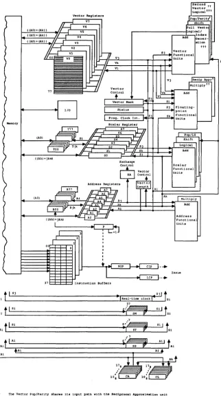
Each CPU has independent control and computation sections. All CPUs share Central Memory and the inter-CPU communication and 1/0 sections. (CPU sections are described in later sections.) Figure 1-2 shows the mainframe chassis. Figure 1-2 illustrates the basic organization of the computer; figure 1-3 illustrates the components and control and data paths of each CPU in the system.
CPU COI'I!IUIIlCATION
CONTROL SBCTION SBCTION CONTROL SECTION
·
Instruction·
Shared Registers·
InstructionBuffers Buffers
·
Semaphore·
COntrol Registers·
COntrolRegisters Registers
·
Real-tiJlle Clock·
Bxchange Register·
BxchangeMechanism Mechanism
r - - • Interrupt
V
~
·
Interrupt-·
Programmable COMPUTATION COMPUTATION·
ProgrammableClock SECTION SBCTION Clock
·
Status -·
Registers·
Register-.
StatusRegister Register
·
Functional·
Functionalunits Units
I
r - -
-MBMORY SECTION 4, 8, or 16 million
64-bi t words
CONTROL SBCTION I - - - - CONTROL SECTION
·
Instruction·
InstructionBuffers Buffers
·
COntrol·
ControlRegisters Registers
·
Bxchange·
BxchangeMechanism Mechanism
·
Interrupt·
Interrupt·
Programmable COMPUTATION COMPUTATION·
ProgrammableClock SBCTION SBCTION clock
·
Status -·
Registers·
Register-.
StatusRegister register
·
Functional·
Functionalunits units
I
1/0 SBCTIONI
·
Four 6 Mbyte per second channel pairs·
Two 1250 Mbyte per second channel pairs·
Four 100 Mbyte per second channel pairs [image:15.613.126.488.310.642.2]((AO)+(Ak)) ( (AO) + (Ak))
( (Ah)+jkm)
(AO)
37
Si
t
I SjVector Req1sters
V7
V6 VS
Instruction Buffers
ExchanO'e Control
• . S j !
t
I Real-time clock I Si37
Si
t
LI.:S:.i _ _ _ _ _ _ _ _ _ _ _ _ _ _ _ _ _ _ _ ~~~·t··~=:==9t"_-.:;.Si::...l1 tSi
_
i5M---v
_
Second t t
Vector
Loq1cal t t t
Add
Add
Scalar
Funct 1 onal Units
Gener-ation
t t t
Multiply
Add
Address Functiona Units
Issue
SitLi~S~i---~r==S~T==~-~S~1! tSi
Ai
Ai~ __ ~---~~~~----~~ Ai
Ai
The Vector Pop/Parity shares It.s input path with the Reciprocal Approximation unit
t t The Second Vector Loqical shares its input and output path with the Floatinq-point Multiply unit.
ttt Second Vector LOQ'ical and Index Generation units are not available on all systems.
Ak
[image:16.615.149.471.52.628.2]INTERFACES
The Cray mainframe is designed for use with front-end computers in a
computer network.
A front-end computer system is self-contained and
executes under the control of its own operating system.
Standard interfaces connect the Cray mainframe's
1/0channels to channels
of front-end computers, providing input data to the Cray mainframe and
receiving output from it for distribution to peripheral equipment.
Interfaces compensate for differences in channel widths, machine word
size, electrical logic levels, and control signals.
(The Master
1/0Processor (MIOP) of the lOS communicates with the mainframe through a 6
Mbyte per second channel pair to a channel adapter module in the Cray
mainframe.)
Typically, communication continues through a front-end
interface to the front-end computer typically through a front-end
computer
1/0channel.
A stand-alone cabinet houses the front-end interface (figure 1-4) located
near the host computer.
Its operation is invisible to the front-end
computer user and the Cray user.
A primary goal of the interface is to maximize the use of the front-end
channel connected to the Cray system.
Since the MIOP channel connected
to the interface is faster than any front-end channel connected to the
interface, the burst rate of the interface is limited by the maximum rate
of the front-end channel.
Interfaces to front-end computers allow the front-end computers to
service the Cray computer system in the following ways:
•
As a master operator station
•
As a local operator station
•
As a local batch entry station
•
As a data concentrator for multiplexing several other stations
into a single Cray channel
•
As a remote batch entry station
•
As an interactive communication station
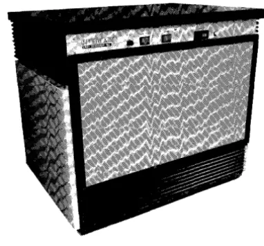
Figure 1-4. Typical Interface Cabinet
1/0 SUBSYSTEM
The lOS, shown in figure 1-5, is standard on the CRAY X-MP system and has two, three, or four rops, Buffer Memory, and required interfaces. The lOS is designed to provide fast data transfer between its Buffer Memory and the mainframe's Central Memory as well as front-end computers, peripheral devices, and storage devices.
Four types of lOPs may be configured in an ros: an MIOP, a Buffer lOP (BIOP), a Disk lOP (DIOP), and an Auxiliary lOP (XIOP). All lOSs must have at least one MIOP and one BIOP. The number of DIOPs and XIOPs is site dependent.
Each lOP of the lOS has a memory section, a control section, a
computation section, and an inputloutput (1/0) section. 110 sections are
independent and handle some portion of the 1/0 requirements for the lOS.
Each lOP also has six direct memory access (DMA) ports to its Local Memory.
The MIOP controls the front-end interfaces and the standard group of stationt peripherals. The Peripheral Expander interfaces the station peripherals to one DMA port of the MIOP. The MIOP also connects to
[image:18.617.199.390.125.302.2]The BIOP is the main link between the mainframe's Central Memory and the
mass storage devices.
Data from mass storage is transferred through the
BIOP's Local Memory to the mainframe's Central Memory through a 100 Mbyte
per second channel pair.
The DIOP is used for additional disk storage units (DSUs).
This
processor can handle up to four disk controller units (DCUs) with up to
16 disk storage units.
The DIOP uses one DMA port for each controller,
one DMA port to connect to Buffer Memory, and another DMA port to connect
a 100 Mbyte per second channel pair to the mainframe Central Memory.
The XIOP is used for block multiplexer channels and interfaces to a
maximum of four BMC-4 Block Multiplexer Controllers.
Each controller can
handle up to four block multiplexer channels.
The XIOP uses one DMA port
for each controller and another DMA port to connect with Buffer Memory.
IDS hardware allows for simultaneous data transfers between the BIOP,
MIOP, and DIOP, or XIOP of the lOS and the mainframe's Central Memory.t
Section
2describes the CPU I/O section for the system.
Refer to the I/O
Subsystem Hardware Reference Manual for a complete description of the lOS.
DISK STORAGE UNITS
For mass storage, the system uses CRI disk storage units.
A disk
controller unit interfaces the disk storage units with an lOP of an IDS
through one DMA port.
Up to four disk storage units can be connected to
a single disk controller unit.
The lOP and the disk controller unit can transfer data between the DMA
port and four disk storage units with all disk storage units operating at
full speed without missing data or skipping revolutions.
A m~n~mumof
2and a maximum of 48 disk storage units can be configured on an IDS.
The
IDS chassis houses the disk controller unit.
Each disk storage unit has two accesses for connecting it to
controllers.
The second independent datapath to each disk storage unit
exists through another CRI controller.
Reservation logic provides
controlled access to each disk storage unit.
Dynamic sharing of devices
is not supported by the Cray operating system COS software.
The Disk
Systems Hardware Reference Manual includes further information about the
mass storage subsystem.
SOLID-STATE STORAGE DEVICE
The SSD, shown in figure 1-6, is used for temporary data storage and
transfers data to and from the mainframe's Central Memory.
The transfer
speed is dependent on the SSD memory size and configuration as described
in the SSD Solid-state Storage Device Hardware Reference Manual.
The
maximum speed attained from the SSD to Central Memory is
1250Mbytes/s
[image:21.612.123.477.204.626.2]CONDENSING UNITS
Condensing units (figure 1-7) contain the major components of the
refrigeration system used to cool the computer chassis and consist of two 25-ton condensers. Heat is removed from the condensing unit by a
second-level cooling system that is not part of the computer system. Freon, which cools the computer, picks up heat and transfers it to water in the condensing unit.
POWER DISTRIBUTION UNITS
The Cray mainframe, IDS, and SSD all operate from 400-Hz, three-phase power. The mainframe, IDS, and SSD have independent power distribution units.
The power distribution unit for the mainframe contains adjustable
transformers for regulating the voltage to each column of the mainframe. The power distribution unit also contains temperature and voltage
monitoring equipment that checks temperatures at strategic locations on the mainframe chassis. Automatic warning and shutdown circuitry protects .the mainframe in case of overheating or excessive cooling. Control
switches for the motor-generators and the condensing unit are mounted on the mainframe power distribution unit.
A smaller power distribution unit performs similar functions for the IDS chassis or the SSD chassis.
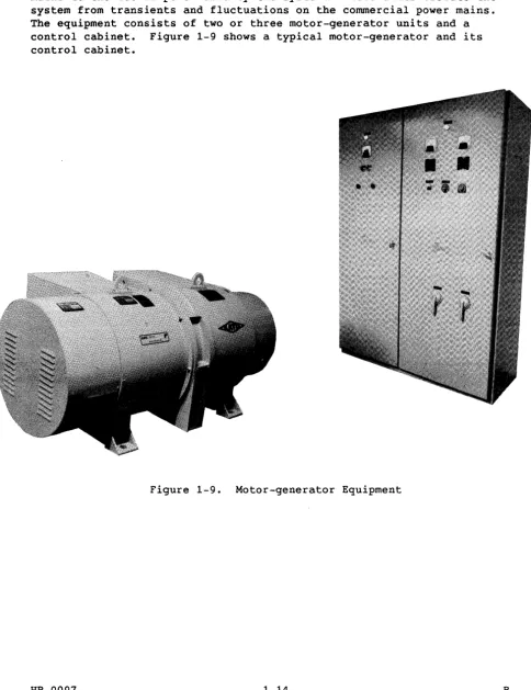
[image:23.613.388.496.341.647.2] [image:23.613.99.312.342.641.2]MOTOR-GENERATOR UNITS
The motor-generator units convert primary power from the commercial power
mains to the 400-Hz power used by the system.
These units isolate the
system from transients and fluctuations on the commercial power mains.
The equipment consists of two or three motor-generator units and a
control cabinet.
Figure 1-9 shows a typical motor-generator and its
control cabinet.
[image:24.618.59.543.102.731.2]I
SYSTEM CONFIGURATION
Figures 1-10 and 1-11 illustrate two configurations for the CRAY X-MP four-processor computer systems.
Front-end Computers
Front-end Interfaces
To mainframe or I/O Subsystem
CRAY X-MP mainframe 4, 8, or 16 Million
64-Bit Words
SSD
/(J~I - 09
--
Cray 6 Mbyte channel Cray 100 Mbyte channel . . . . Cray 1250 Mbyte channelFigure 1-10. Block Diagram of a Typical Four-processor System
I
1 to 4
Front-end Computers
Front-end Interfaces
To mainframe or I/O Subsystem
Block Multiplexer - - 1 TO 8 Channels Controllers
CRAY X-MP mainframe 4, 8, or 16 Million
64-Bit Words
SSD
IDSJ " / 0
--
Cray 6 Mbyte channel Cray 100 Mbyte channel . . . . Cray 1250 Mbyte channelCPU RESOURCES
All four central processing units (CPUs) share the mainframe's Central Memory, the inter-CPU communication section, and the inputloutput (1/0)
section. The following pages describe these areas common to all CPUs.
CENTRAL MEMORY
Central Memory consists of a number of banks of solid-state, random-access memory (RAM) and is shared by the CPUs and the 1/0
section. Three Central Memory sizes are available with either 16K- or
2
I
64K-chip technology: 4 million words with 32 banks (64K chips),8 million words with either 32 banks (64K chips) or 64 banks (16K chips), or 16 million words with 64 banks (64K chips). Banks are independent of each other; sequentially addressed words reside in sequential banks. Each word is 72 bits, with 64 data bits and 8 check bits.
I
Central Memory cycle time takes 4 clock periods (CPs) to execute. Access time, the time required to fetch an operand from Central Memory to anI
operating register, is 14 CPs for address (A) and scalar (S) registers.I
Access time is 17 CPs plus vector length for a vector (V) register and 16 CPs plus block length for a block transfer to a intermediate address (B) or intermediate scalar (T) register.
The maximum transfer rate per CPU for B, T, and V registers is 3 words per CP; for A and
S
registers per CPU, i t is 1 word every 2 CPs.Transfer of instructions to instruction buffers occurs at a rate of 32 parcels (8 words) per CPo For the 1/0 section, the transfer rate is
4 words per CPo
Central Memory features are summarized and are described in detail in the following paragraphs.
• Shared access from all CPUs
• 4 million, 8 million, or 16 million words of integrated circuit memory, using 16K or 64K chips
• 64 interleaved banks • 4-CP bank cycle time
• Single-error-correction/double-error-detection (SECDED)
• 3 words per CP transfer rate to B, T, and V registers per CPU • 1 word per 2-CP transfer rate to A and S registers per CPU
• 8 words per CP transfer rate to instruction buffers
• 4 words per CP transfer rate to IIO concurrent with all memory activity except instruction fetch and exchange
MEMORY ORGANIZATION
Memory is organized to provide fast, efficient access for all CPUs. Data transfers to and from memory are corrected with SECDED. Central Memory is organized into four sections with 16 banks in each section.
Each CPU
is
connected to an independent access path into each of the four sections, as shown in figure 2-1. This configuration allows up to 16 memory references per CPoSECTION 2 SECTION 0
Banks 10-13, Banks 0-3,
30-33t, 50-53, 20-23t, 40-43,
70-73 60-63
f
CPU CPU
Path Path
,--. Selection Selection
A
BI
cl
A BI
CI
CPU CPU
Ports Ports I/O
CPU CPU
Ports Ports
A
'I 'I
A'I 'I
CPU CPU
-Path Path
Selection Selection
t
SECTION 3 SECTION 1
Banks 14-17, ~ Banks 4-7,
34-37t, 54-57, 24 -27t, 44-47,
74-77 64-67
lOS,"
[image:28.615.160.451.307.647.2]MEMORY ADDRESSING
Memory addressing is dependent on system memory architecture (chip size and number of banks) and memory size. The following paragraphs describe the memory addressing for the four-processor system.
Memory addressing for 32-bank, 64K-chip, 4-million-word system
A word in a 32-bank, 64K-chip memory is addressed in a maximum of 21 bits, as shown in table 2-1. The low-order 5 bits specify one of the 32 banks. The next 16-bit field specifies an address within the chip. The high-order 2 bits specify one chip on the module.
Memory addressing for 64-bank, 16K-Chip, 8-million-word system
memory is addressed in a maximum of 22 A word in a 64-bank, 16K-Chip
bits, as shown in table 2-1. banks. The next 14-bit field high-order 3 bits specify one
The low-order 6 bits specify one of the 64 specifies an address within the chip. The chip on the module.
Memory addressing for 32-bank, 64K-chip, 8-million-word system
A word in a 32-bank, 64K memory is addressed in a maximum of 22 bits, as shown in table 2-1. The low-order 5 bits specify one of the 32 banks. The next 16-bit field specifies an address within the chip. The
high-order 2 bits specify one chip on the module.
Memory addressing for 64-bank, 64K-chip, 16-million-word system A word in a 64-bank, 64K-chip memory is addressed in a maximum of 23 bits, as shown in table 2-1. The low-order 6 bits specify one of the 64 banks. The next 16-bit field specifies an address within the chip. The high-order 2 bits specify one chip on the module.
MEMORY ACCESS
Each CPU in the system has four memory access ports, referred to as Port A, Port
B,
Port C, and I/O. Each port is capable of making one reference per CPo Ports A, B, and C are used for CPU register transfers.• Vector store, B, or T store instructions (111, 035, and 031) and scalar instructions (100 through 131) use Port C
Once an instruction issues to a port, that port is reserved until all references are made for that instruction.
Table 2-1. Memory Addressing Formats
Chip Central No. of No. of
Type Memory Banks Columns Address Format
16K 8 64 12 222 2 19 25
Chip Internal bit 6-bit address address in bank select chip
64K 4 32 12 221 220 24
Chip Internal bit 5-bit address address in bank select chip
64K 8 32 12 222 220 24
Chip Internal bit 5-bit address address in bank select chip
64K 16 64 12 223 221 25
Chip Internal bit 6-bit address address in bank select chip
20
20
2 0
20
The references for each element of a block transfer (V, B, or T) are made and completed in sequence through a port. However, since each reference is examined individually for possible conflicts, the data flow for a
NOTE
Because concurrent block reads and writes are not
examined for memory overlap hazard conditions (that is, read before write or write before read), the software must detect where this condition occurs and ensure sequential operation.
The bidirectional memory mode enable (002500), bidirectional memory mode disable (002600), and the complete memory reference (002700) instructions are provided to resolve these cases and assure sequential operation. If the bidirectional memory mode is clear, block reads and writes are not allowed to operate concurrently within that CPU. Instruction 002700 allows the program to wait until the last references of all preceding block transfers are past the conflict resolution stage within the CPU issuing it and the transferred data is being transmitted to the
designated memory or register locations. Instruction 002700 provides software a mechanism, wherever necessary in the program, to guarantee sequential memory operation within a CPU or between CPUs.
Issue of scalar memory references requires Ports A, B, and C to be available, ensuring sequential operation between block transfers and scalar references within a CPu.
A scalar reference ~onflict is detected in CP 4 of execution. If a conflict occurs, two more scalar references are allowed to issue. A fourth scalar reference holds issue if the conflict condition still exists for the first scalar reference.
Scalar references always execute in the order they are issued within a CPU. Instruction 002700 detects when all scalar references are past the conflict resolution stage within the CPU issuing it.
An I/O channel references memory through a specific CPU's I/O port (refer to the subsection on CPU Input/Output). The I/O port can be active
regardless of the activities on Ports A,
B,
or C.For instruction fetches and exchange sequences, the CPUs are allowed access to memory in pairs; CPUs 0 and 1 comprise one pair,CPUs 2 and 3 another pair. Only one instruction fetch or exchange sequence can occur among the four CPUs at a time.
NOTE
A fetch sequence that follows a scalar store can, under certain conditions, complete before the store. For this to happen, however, an out-of-buffer condition must arise before the scalar store is in CP 2 of execution. The out-of-buffer condition can occur before the scalar store is in CP 2 of execution if a buffer boundary is crossed without doing a branch. This presents a problem only if the fetch and store are to the same area in memory. Therefore, software that utilizes dynamic coding should ensure that the code generated is actually in memory before that area of memory is fetched into the instruction buffers.
During this time, the other CPU pair has access to the remaining banks of memory.
When a CPU requests an exchange, all referencing from the four memory ports of the other CPU in the CPU pair is inhibited and 32 banks are reserved (to prevent referencing from the other CPU pair). When memory is quiet (0 to 3 CPs), the exchange proceeds and references 16 banks in the next 20 CPs. Each bank is referenced twice during this time, once for a read and once for a write. An exchange sequence requires all activities within a CPU to complete before the exchange request is made. As with the instruction fetch, the other CPU pair has access to the
remaining banks of memory.
A fetch request follows immediately after the exchange is complete and then referencing from the memory ports of the other CPU in the pair is enabled.
Conflict resolution
During each CP, references to the memory ports in the system are examined for memory access conflicts. If a conflict occurs for a reference, the reference is held and no further referencing from that port is allowed until the conflict is resolved.
Bank Busy conflict - The Bank Busy conflict is caused by any port within or between CPUs requesting a bank currently in a reference cycle.
Resolution of this conflict occurs when the bank cycle is complete. All ports in the CPU are held 1, 2, or 3 CPs because of a Bank Busy conflict.
Simultaneous Bank conflict - The Simultaneous Bank conflict is caused by two or more ports in different CPUs requesting the same bank. Resolution of this conflict is based on a priority (refer to
subsection on Memory access priorities). All ports in a CPU are held 1 CP because of a Simultaneous Bank conflict. A Bank Busy conflict always follows a Simultaneous Bank conflict.
Section Access conflict - The Section Access conflict is caused by two or more ports in the same CPU requesting any bank in the same
section. Resolution of this conflict is based on priority. The highest priority port is allowed to proceed, all other ports involved in this conflict hold (refer to subsection on Memory access
priorities). The port is held 1 CP because of a section access conflict.
Memory access priorities
The following priorities are used to resolve memory access conflicts.
• Intra-CPU priority: the priority between Ports A, B, and C is determined by the following conditions:
Any port with an odd increment always has a higher priority than a port with an even increment, regardless of their issued sequence.
Among all ports with the same type of increment (odd or even), the relative time of issue determines the priority, with the first issued having the highest priority.
• Inter-CPU priority: every 4 CPs the priority between CPUs changes.
• 1/0 priority: the 1/0 ports are always lowest priority, within CPUs.
MEMORY ERROR CORRECTION
Data Bits
o
63 64 Check Bits 11
'" '" '"
-
~Data Fanin Error CPU
Correct Memory
~
Error '" Detect
~
Figure 2-2. Memory Datapath with SECDED
If a single bit of a data word is altered, the single error alteration is automatically corrected before passing the data word to the computer. If 2 bits of the same data word are altered, the error is detected but not corrected. In either case, the CPU can be interrupted, depending on interrupt options selected to allow processing of the error. For 3 or more bits in error, results are ambiguous.
The SECDED error processing scheme is based on error detection and correction codes devised by R. W. Hamming.t An 8-bit check byte is appended to the 64-bit data word before the data is written in memory. The 8 check bits are generated as even parity bits for a specific group of data bits. Figure 2-3 shows the bits of the data word used to
determine the state of each check bit. An X in the horizontal row
indicates that data bit contributes to the generation of that check bit. Thus, check bit 0 is the bit that makes group parity even for the group of bits 21, 2 3 , 2 5 , 21, 2 9 , 211, 213 , 2 15 , 211, 2 19 , 221, 2 23 , 2 25 , 221, 2 29 , and 2 31 through 255.
The 8 check bits and the data word are stored in memory at the same
location. When read from memory, the same 64-bit matrix of figure 2-3 is used to generate a new set of check bits, which are compared with the old check bits. The resulting 8 comparison bits are called syndromett bits
(S bits). The states of these S bits are all symptoms of any error that occurred (1=No compare). If all syndrome bits are 0, no memory error is assumed.
Any change of state of a single bit in memory causes an odd number of syndrome (S) bits to be set to 1. A double error (an error in 2 bits) appears as an even number of syndrome bits set to 1.
The matrix is designed so that:
• If all S bits are 0, no error is assumed.
• If only 1 S bit is 1, the associated check bit is in error.
• If more than 1 S bit is 1 and the parity of S bits SO through S7 is even, a double error (or an even number of bit errors) occurred within the data bits or check bits.
•
If more than 1 S bit is 1 and the parity of all S bits is odd, a single and correctable error is assumed to have occurred. The S bits can be decoded to identify the bit in error.•
If 3 or more memory bits are in error, the parity of all S bits is odd and results are ambiguous.Modules involved with generating and interpreting the 8-bit check byte used for SECDED include logic that can be used for verifying check bit storage, check bit generation, and error detection and correction. Refer to appendix D for information on SECDED maintenance functions.
check bi t 0
check bi t 1
check bit 2
check bi t 3
check bi t 4
check bi t 5
check bi t 6 check bit 7 x
x
x x
CHECK BYTE
x x
x
x x
x
x x
x x
x x
x
x x x
x x
x
x x x x
x x
x
x x
x
x x
x x
x x
INTER-CPU COMMUNICATION SECTION
The inter-CPU communication section of the system contains special hardware for communication among the CPUs, for control, and for a
Real-time Clock (RTC). The RTC, Shared Address (SB), Shared Scalar (ST), and Semaphore (SM) registers are shared by the CPUs. These registers with their sources and destinations are shown in figure 2-4 and described
in the following paragraphs.
~~ ---»-~I
RTC~I .---~»--- ~~
Ai Ai
t----r= ... ~~---... - SBj
Si
STj
Si Si
SM~_~----~~~~_.
'v ~+---~~---~--SMJ
Figure 2-4. Shared Registers and Real-time Clock
REAL-TIME CLOCK
Instructions used with the RTC register are: Octal Code
0014jO 072iOO
CAL Syntax RT Sj
Si
RTDescription
Enter the RTC register with (Sj)
Transmit (RTC) to
Si
A program reads the CP counter using instruction 072 and resets i t with instruction 0014jO. Loading or reading the CP counter can occur from all CPUs simultaneously time. If more than one CPU is in monitor mode, the software should ensure that only one CPU enters a value into this register.
INTER-CPU COMMUNICATION AND CONTROL
Five identical sets of shared registers are used for communication and control among CPUs. Each set contains eight 24-bit Shared Address (SB) registers, eight 64-bit Shared Scalar (ST) registers, and 32 1-bit Semaphore (SM) registers.
Each CPU's Cluster Number (CLN) register determines which set of shared registers is accessed by a CPU (clustering). The CLN register is loaded from the Exchange Package or, if the CPU is in monitor mode, through instruction 0014j3.
The CLN register can contain one of six different values. Values 1, 2, 3, 4, or 5 allow the CPU to access one of the five sets of shared
registers. Value 0 prevents any access to shared registers by the CPU. If the value is 0, instructions regarding the shared registers become no-ops, except for the instructions returning values to
Ai
orSi,
which return a zero value. If the CLN registers in more than one CPU are set to the same value (1, 2, 3, 4, or 5), then those CPUs share a common set of SB, ST, and SM registers.
Shared Address and Shared Scalar registers
The SB and ST registers are used for passing address and scalar
The instructions used with the SB and ST registers are: Octal Code CAL Syntax Description
026ij7
AiSBj
Transmit(SBj)
to Ai027ij7
SBj
Ai Transmit (Ai) toSBj
072ij3
si STj
Transmit(STj)
toSi
073ij3
STj Si
Transmit(Si)
toSTj
Semaphore registers
The SM registers are used for control among the CPUs. No hardware reservations are made on these registers. Loading or reading the SM registers or setting or clearing a particular SM register can occur at any time from any or all CPUs.
The test and set instruction
(0034jk)
is the only operation on the SM registers including a hardware interlock. This interlock prevents a simultaneous test and set operation on the same SM register from more than one CPU. The test and set instruction first tests the value of the selected SM register. If the value is 0, the instruction issues and sets that SM register to a 1. If the value is 1, the instruction holds issue until the value iso.
When all CPUs in a cluster are holding issue on a test and set
instruction, a deadlock interrupt can occur. All CPUs with equal cluster numbers above 0 belong to the same cluster and must be holding issue on a test and set instruction to cause a deadlock interrupt. When that
happens, all CPUs in the cluster receive deadlock interrupts. If only one CPU belongs to a cluster and holds issue on a test and set
instruction, that CPU receives a deadlock interrupt. No deadlock interrupt can occur in cluster 0 (CLN=O).
When an interrupt occurs, normally the instructions already in the Next Instruction Parcel (NIP) and Current Instruction Parcel (CIP) registers are allowed to issue before the exchange sequence starts. If a test and set instruction is holding in the CIP register and an interrupt occurs, a special exchange start-up sequence is initiated. Here, the instruction in the NIP register and the test and set instruction in the CIP register are discarded and the Program Counter (P) register is adjusted to point to the discarded test and set instruction. The Waiting on Semaphore (WS) flag in the Exchange Package sets, indicating a test and set instruction was holding in the CIP register when the interrupt occurred. The
exchange sequence is then started.
Octal Code CAL Syntax Description
0031jk
SMjk
1 SetSMjk
012i02
Si
SM Transmit (SM) toSi
013i02
SMSi
Transmit(Si)
to SMShared register and semaphore conflicts
A scanner is used to break a tie caused by simultaneous requests for access to the Semaphores or Shared registers of any cluster. If there is no competition for access, no extra hold issues are generated. For
example, an
021ij1
holds issue 3 CP, but if there is an access conflict, issue holds until a scanner with four slots breaks the tie. A request takes 2 CPs to complete; therefore, subsequent requests can be accepted every other CP until all requests are resolved.CPU INPUT/OUTPUT SECTION
The I/O section of the mainframe is shared by all CPUs. The mainframe supports three channel types identified by their maximum transfer rates of 1250 Mbytes per second, 100 Mbytes per second, and 6 Mbytes per second. Two 1250 Mbyte per second channel pairs transfer data between Central Memory and an SSD. These channels are 128 bits wide and use 16 check bits in each direction. A maximum transfer rate of more than 10 gigabits per second is possible on a 1250 Mbyte per second channel. The channel is two parallel 64-bit channels each with SECDED; therefore, under certain circumstances the full-width channel can correct double errors. Four 100 Mbyte per second channel pairs transfer data between Central Memory and an I/O Subsystem. A 100 Mbyte per second channel is 64 bits wide and uses 8 check bits in each direction. Data words are transferred
in blocks of 16 under the control of Data Ready and Data Transmit control signals. Each 100 Mbyte per second channel has a maximum transfer rate of approximately 850 Mbits per second.
lOS communication with the CPUs is over four pairs of control channels, each with a maximum transfer rate of 6 Mbytes per second. Each 6 Mbyte per second channel is 16 bits wide.
• Two channel pairs with a 1250 Mbytes per second maximum
transfer rate per channel; 128 data bits and 16 check bits in each direction.
• Four channel pairs with a 100 Mbytes per second maximum transfer rate per channel; 64 data bits, 3 control bits, and
8 check bits in each direction.
• Four 1/0 channel pairs with a 6 Mbytes per second maximum transfer rate per channel
Shared control from the CPUs
16 data bits, 3 control bits, and 4 parity bits in each direction
Lost data detection
• Channels are divided into four groups; each group contains either input or output channels.
• Channel groups are served equally by memory (each group is scanned every 4 CPs).
• Channel priority is resolved within channel groups.
DATA TRANSFER FOR SOLID-STATE STORAGE DEVICE
Data is transferred directly between the SSD and the mainframe using the 1250 Mbyte per second channels. A 1250 Mbyte per second channel is 128 bits wide and is programmed through software. The SSD Solid-state Storage Device Hardware Reference Manual contains programming details for the SSD.
DATA TRANSFER FOR 1/0 SUBSYSTEM
A 100 Mbyte per second channel pair transfers data between Central Memory and the BIOP of the lOS. A second 100 Mbyte per second channel pair transfers data between Central Memory and a DIOP or XIOP.t Each
channel is 64 bits wide and handles data at approximately 100 Mbytes/s. Each channel uses an additional 8 check bits for SECDED, as is used in Central Memory.
The CPU side of a 100 Mbyte per second channel pair uses a pair of
16-word buffers to stream the data out of Central Memory and another pair to stream data into Central Memory. On output, as one buffer block is being sent to the lOP, the other buffer is filling from Central Memory. Similarly, on input, one buffer block is filling from an lOP while the other is transmitting to Central Memory.
At the lOP side of a 100 Mbyte per second channel pair, data passing into Local Memory (an IOP's memory) is double buffered and disassembled into 16-bit parcels. The channel side passing data from Local Memory simply assembles 16-bit parcels into 64-bit words for transmission to a CPU. An lOP controls a 100 Mbyte per second channel pair linking i t with Central Memory. The lOP initiates all data transfers on the channel and performs all error processing required for the channel. There are no CPU instructions for the 100 Mbyte per second channel pair. The 1/0
Subsystem Reference Manual contains programming details for the 100 Mbyte per second channels.
6 MBYTE PER SECOND CHANNELS
Standard control channels for the system are 6 Mbyte per second channels. Each 6 Mbyte per second channel has 16-bit asynchronous
control logic used for front-end interfaces. The instructions used with 6 Mbyte per second channels follow.
Octal Code CAL Syntax
0010jk CA,Aj Ak
0011jk CL,Aj Ak
0012jk CI,Aj
033iOO Ai CI
033ijO Ai CA,Aj
Description
Set the Current Address (CA) register for the channel indicated by (Aj) to (Ak) and activate the channel
Set the channel Limit Address (CL) register for the channel indicated by (Aj) to (Ak)
Clear the Interrupt flag and Error flag for the channel indicated by (Aj): Output channel k=O; clear MC, k=l; set MC. Input channel k=O; no operation, k=l; clear held ready.
Transmit channel number to Ai
MULTI-CPU PROGRAMMING
The 6 Mbyte per second I/O channels can operate from any CPU, and any CPU can issue instructions to any of the channels. There is no hardware interlock among theCPUs; therefore, software must ensure that only one CPU is servicing I/O at a time while in monitor mode. Instruction 033 is independent in nature and can be issued without an interlock.
The following conditions must be met for an I/O interrupt to occur:
• No CPU waiting for an exchange • No CPU in monitor mode
• An interrupt is present
Normally, the interrupt from a 6 Mbyte per second channel is directed toward the CPU that last issued a clear interrupt instruction (0012) to that channel. Because an I/O interrupt occurs, however, in only one CPU at a time, the following conditions (in priority order) determine the CPU toward which the interrupt is directed. Once in monitor mode, a CPU should service all I/O interrupts.
1. All I/O interrupts are directed toward a CPU that has the select external interrupt mode set.
2. If no CPU has selected external interrupts, then interrupts are directed toward a CPU holding issue on a test and set instruction. 3. If neither conditions 1 nor 2 exist or if they exist in all CPUs,
the interrupt is directed to the CPU that last issued a clear interrupt instruction to that channel.
6 MBYTE PER SECOND CHANNEL OPERATION
Input and output channels access Central Memory directly. Input channels store external data in memory and output channels read data from memory. A primary task of a channel is to convert 64-bit Central Memory words into 16-bit parcels or 16-bit parcels into 64-bit Central Memory words. Four parcels make up one Central Memory word with bits of the parcels assigned to memory bit positions as shown in table 2-2. In both input and output operations, parcel 0 is always transferred first.
Each input or output channel has a data channel (4 parity bits, 16 data bits, and 3 control lines), a 64-bit assembly or disassembly register, a channel CA register, and a channel CL register.
I/O interrupts can be caused by the following:
• On all output channels, if (CA) becomes equal to (CL), then the resume for the last parcel transmitted sets interrupt.
• External device disconnect is received on any input channel and channel is active.
• Channel error condition occurs (described later in this section) •
Table 2-2. Channel Word Assembly/Disassembly
Number
Characteristic Bit Position of Bits Comment
Channel data bits 2 15 _2° 16 Four 4-bit groups Channel parity bits 4 One per 4-bit group CRAY X-MP word 2 63 _2° 64
Parcel
° 2 63 _2 48 16 First in or out
Parcel 1 2 47 _2 32 16 Second in or out Parcel 2 2 31 _2 16 16 Third in or out Parcel 3 2 15 _2° 16 Fourth in or out
The number of the channel causing an interrupt can be determined by using instruction 033, which reads into Ai the highest priority channel number requesting an interrupt. The lowest numbered channel has the highest priority. The interrupt request continues until
cleared by the monitor program when an interrupt from the next highest priority channel, if present,
is
sensed. All interrupts are available through instruction 033 to all CPUs. Channel numbers for 6 Mbyte per second channels arelOa
through 178 (10/11, 12/13, 14/15, and16/17; even for input, odd for output).
INPUT CHANNEL PROGRAMMING
To start an input operation, the CPU program (refer to figure 2-5):