N A N O E X P R E S S
Open Access
High-Efficiency Plasmonic Third-Harmonic
Generation with Graphene on a Silicon
Diffractive Grating in Mid-infrared Region
Junhao Li
1, Tian Zhang
2and Lin Chen
1*Abstract
Benefiting from the large third-order nonlinear susceptibility of graphene and significantly enhanced field intensity of graphene plasmons (GPs), graphene has shown great potentials to enhance plasmonic third-harmonic
generation conversion efficiency. However, it still lacks an effective configuration that can excite the fundamental frequency (FF) GPs and guide the generated third-harmonic frequency (THF) GPs simultaneously. Here, we have proposed a diffractive silicon grating underneath a graphene sheet to generate and transmit THF GPs. The FF GPs are efficiently excited by illuminating a normal-incidence plane wave due to guided-mode resonance and then are converted to the THF GPs with a large conversion efficiency, originating from the giant field intensity of the FF GPs. We numerically demonstrate that, a large third-harmonic generation conversion efficiency of 3.68 × 10⁻⁷can be realized with a small incident power density of 0.19 MW/cm2at 28.62μm. Furthermore, the generated THF GPs can be efficiently guided along low-loss GP waveguides that are connected to both sides of grating section. Our results can stimulate making graphene-based light sources for mid- and far-infrared silicon photonics.
Keywords:Third-harmonic generation, Graphene, Surface plasmon, Integrated optics
Introduction
Harmonic generation is a nonlinear optical process, in which N photons with the same frequency ω interacting with a nonlinear material are combined to generate new photons with frequencyNω. As a means to extend coherent light sources to short wavelengths, third-harmonic gener-ation (THG) has attracted tremendous research interest. Conventionally, high-efficiency harmonic generation is real-ized in exotic crystals, but which compromises high-density photonic integration [1]. Silicon has become the mature material choice as an optical information carrier to transmit light signals in highly integrated photonic circuits. Nonlin-ear optical effects, such as stimulated Raman scattering [2] and THG [3–5], have great potentials to broaden the func-tionalities of silicon photonics. However, efficient light emission by using silicon remains a challenging issue due to its indirect band gap. Using nonlinear optical interac-tions, such as THG, seems a rather promising approach to
provide coherent light for silicon photonics. In general, the THG conversion efficiency (CE) for an optical waveguide can be enhanced by using phase matching between the fun-damental mode and the third-harmonic mode. This method typically requires complicated configurations, which are usually difficult to implement in practical situa-tions. An effective and robust method for enhancing the THG CE can be made by increasing the light intensity within the nonlinear material, which offers us the oppor-tunity to relax the stringent demanding for the phase-matching condition. This has been recently realized by using ultrahigh quality factor slow light silicon photonic crystals [3–5], small-modal-volume silica microrods [6], and surface plasmons [7–10]. It has been reported that sili-con photonic crystals have improved the THG CE to the magnitude of ~ 10−7due to the reduced group velocity of c/40 [4]. Quite recently, surface plasmons have been proved capable of increasing the THG CE to the order of 10−5due to the tight electric field enhancement [7].
In recent years, the operation wavelength of silicon pho-tonics has extended to the mid- and far-infrared (IR) re-gions due to many potential applications such as chemical
* Correspondence:[email protected]
1Wuhan National Laboratory for Optoelectronics, Huazhong University of
Science and Technology, Wuhan 430074, China
Full list of author information is available at the end of the article
and biological sensing [11]. The use of plasmonics in mid-and far-IR regions is attractive because the propagation loss of a plasmonic waveguide decreases dramatically at longer wavelengths and also because the mode cross sec-tion of such waveguides is subwavelength, which would significantly enhance light-matter interactions such as THG conversion [7–10, 12, 13]. Recent studies have proved that graphene serves as an excellent nonlinear op-tical material to enhance the nonlinear effect, leading to various applications including four waves mixing [14, 15], THG [16–18], all-optical switching [19], and optical bist-ability [20,21], due to its large third-order nonlinear optical susceptibility. Especially, the observed threshold of optical bistability can be greatly reduced, thanks to the large third-order nonlinear optical susceptibility of graphene [20, 21]. More interestingly, in contrast to plasmon mode in metals, graphene plasmons (GPs) have significantly larger wave vectors as well as much higher confinement of light, which indicates the capability of further enhancing the CE of THG [13]. However, a direct coupling between the fun-damental frequency (FF) GPs and radiation waves is pre-vented due to their momentum mismatch, which makes implementing this scheme a difficult issue in practice. It is for this reason that the researchers have employed the guided-mode resonance of gratings to address the coupling issue [12,18,20]. The proposed scheme in Ref. [18] is pur-posely designed to directly excite the FF GPs and hence en-hance the CE of third-harmonic frequency (THF) free-space waves in the terahertz domain.
In this article, we have also used the guided-mode resonance of gratings to efficiently excite the FF GPs on the graphene sheets. Different from the configur-ation in Ref. [18] where the GPs are used to enhance the CE of THF free-space waves in the terahertz do-main, here, the GPs are utilized to generate THF GPs at infrared frequencies on a silicon chip. The giant field intensity of FF GPs in combination with large third-order nonlinear susceptibility of graphene results in a noticeably enhanced CE of THF GPs on the graphene sheet in mid- and far-IR regions. We note a previous study on using quasi-phase-matching condition to improve the CE of THF GPs on a gra-phene surface [13]. However, we emphasize here, al-though a high CE between FF and THF GP is achievable in Ref. [13], a direct coupling between the radiative waves and GPs is missing. In contrast, the presented scheme not only can directly be coupled with the spatial FF waves, but also can highly effi-ciently generate the THF GPs, rendering the pro-posal suitable for integration on a silicon photonic platform. In addition, the demonstrated plasmonic frequency converters have the advantages of com-pactness and high CE, while requiring a small inci-dent power [22, 23].
Methods
Graphene’s surface conductivity can be estimated by widely used Kubo formula under the assumption of chemical potential (also termed as Fermi energy), μc. In the infrared and terahertz frequencies, with |μc|≫kBT (kB is Boltzmann constant, and T is the temperature), the surface conductivity of graphene could be approxi-mated as
σg¼i e 2k
BT πℏ2ðωþiτ−1Þ
μc kBTþ
2 ln exp − μc kBT
þ1
þi e 2
4πℏ ln
2j j−μc ℏðωþiτ−1Þ 2j j þμc ℏðωþiτ−1Þ
ð1Þ
whereeis the electron charge, ℏis the reduced Planck’s
constant,ωis the radian frequency, andτis the
momen-tum relaxation time representing loss mechanism. In
our study, the working temperature is assumed to beT
= 300 K. By taking the individual graphene sheet as a non-interacting monolayer, the optical conductivity of few-layer graphene isnσg[24], wherenis the number of graphene layers (n< 6). We model graphene as an aniso-tropic material and the effective in-plane permittivity can be written as [25,26].
εx¼εz¼1þ inσgη0
k0dg ð
2Þ
whereη0(=377Ω) is the impedance of air,k0is the wave vector in the air, and dgis the total thickness ofn-layer graphene sheets. The out-of-plane permittivity of gra-phene,εy, is kept constant at 2.5, regardless of the Fermi level [27,28].
Results and Discussion
Excitation of FF GPs with a Silicon Grating
substrate below the grating does not affect the field dis-tribution of the GPs in the air-graphene-grating model. The dispersive relationship of the GPs supported by this configuration can be expressed as [29].
εr1
ffiffiffiffiffiffiffiffiffiffiffiffiffiffiffiffiffi
β2−ε
r1k20
q þ ffiffiffiffiffiffiffiffiffiffiffiffiffiffiffiffiffiεr2 β2−ε
r2k20
q ¼−inσg
ωε0 ð
3Þ
where βis the propagation constant of the GPs along
z-axis,ε0is the permittivity in the air, andεr1(=1) andεr2are the dielectric constants of the dielectric mediums above and below the graphene layers, respectively. As the grating period is much smaller than light wavelength in the air, the silicon grating can be approximately modeled as an ef-fective medium with the equivalent permittivity [30].
εr2¼ fεsiliconþð1−fÞε0 ð4Þ
whereεsilicon(=11.9) is the permittivity of silicon at infra-red and terahertz frequencies [31], andf(=w/p) is the fill-ing ratio of the silicon (fis fixed at 0.5 in this work).
The dispersion relation of the GPs on the GSSDG for different parameters (τ, μc, anddg) is shown in Fig. 2. In the whole work, two-dimensional finite difference time domain (FDTD) with a commercial software of Lumerical FDTD Solution is conducted to do the numerical model-ing. In the simulation of this part, the perfect matched layer boundaries and periodic boundaries are used in they
andzdirections, respectively, while the whole structure is assumed to be infinite along the x direction. The mesh sizes with 0.1 nm alongydirection and 10 nm alongz dir-ection are used to describe the graphene, while non-uniform meshes with a maximum value of 20 nm alongydirection and uniform mesh of 10 nm alongz dir-ection are adopted in the regions besides the graphene sheets. It can be seen from Fig. 2a, d, g that, within the
wavelength range considered, the wave vector of the GPs is dozens of times larger than that of the air, which indi-cates the optical field of the GPs is strongly confined on the graphene surface. However, the phase mismatching between the GPs and the radiation waves prevents the dir-ect coupling between them. The silicon diffractive grating below the graphene sheets shown in Fig.1can provide an additional momentum to overcome the wave vector differ-ence so that the FF GPs can be efficiently excited with a plane wave incidence. The grating period,p, needs to meet the phase-matching equation as
ReðβFFÞ ¼ j2π=pþk0 sinθ ð5Þ
where βFF is the propagation constant of the FF GPs
along z-axis, jis the diffraction order, and θ is the inci-dent angle. To excite the FF GPs of effective wavelength ofλFF with the fundamental diffraction orderj= 1 under
the condition of normal incidence θ= 0, the following
expression should be satisfied
λFF¼ ReðneffÞp ð6Þ
Figure2presents the dependence of the real [Re(neff)] and imaginary [Im(neff)] part of the effective indices and absorption on light wavelength with different values ofτ, μc, anddg. It apparently explains how the parameters of graphene influence the excited FF GPs under the illu-mination of a normal-incidence x-polarized plane wave of FF, where the grating period is fixed at 4μm. Both the real [Re(neff)] and imaginary parts [Im(neff)] of effective refractive indices of the FF GPs decreases with the in-crease of light wavelength within the considered wave-length range (Fig.2a, b, d, e, g, h). This means that, with a shorter wavelength of light, GPs are more strongly confined around graphene sheets, resulting in a larger propagation constant and higher propagation loss. The absorption is highly sensitive to wavelength and is sharply increased as the incident wavelength approaches the resonance wavelength (Fig.2c, f, i). The carrier scat-tering time τ determines the carrier mobility μ in gra-phene as τ¼μμc=eν2
F with the Fermi velocity of νF= 9.5 × 10⁴m/s. Considering that a carrier mobility ofμ> 10 m2V−1s−1 has been experimentally achieved in high-quality suspended graphene [32], which leads to τ> 1.5 ps, our setting of τ≤0.5 ps can reflect the prac-tical transport loss of graphene conservatively. Theτ, as-sociated with the carrier mobility μ, gently influences the Re(neff) and the excitation wavelength of FF GPs, but greatly affects the Im(neff) and absorption (Fig. 2a– c). The enhancedμc decreases Re(neff) and Im(neff) sim-ultaneously, hence reduces the resonance wavelength of FF GPs accordingly (Fig. 2d–f ). The Re(neff), Im(neff), and the resonance wavelength of FF GPs reduce with the
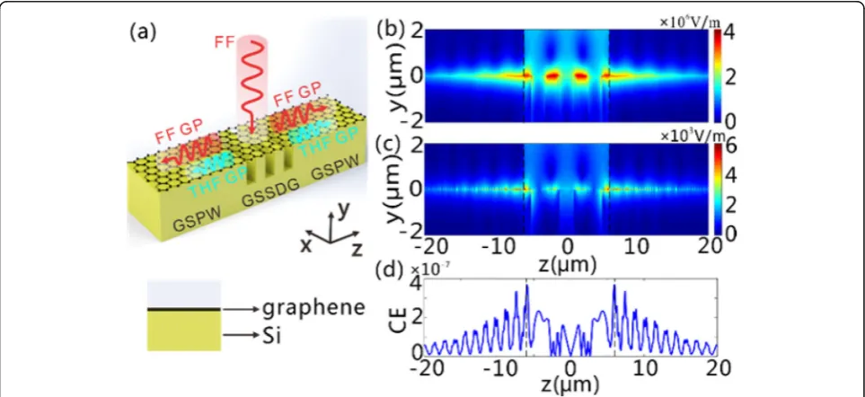
Fig. 1The scheme of the GSSDG as a THG wavelength converter.
[image:3.595.57.291.88.234.2] [image:3.595.73.212.361.391.2]increase of the graphene thickness, corresponding to the number of graphene layers (Fig.2g–i).
In the following, we takeτ= 0.5 ps,μc= 0.65 eV, anddg= 1 nm as examples. The dispersion relation of the GPs on the GSSDG is shown in Fig.3a, where the calculated dis-persion curves agree well with the simulation results ob-tained by the commercial software Lumerical FDTD Solutions. Figure3b shows the optical response of the gra-phene sheets with and without the silicon grating. It can be clearly seen that the absorption efficiency (over 20%) is sig-nificantly enhanced at λ= 28.62 μm when the grating is
involved (p= 4μm). In contrast, the absorption efficiency is kept at a low level (below 2%) over the entire spectral range considered if the grating is not taken into account. The no-ticeably enhanced absorption for the former case can be at-tributed to the excitation of the GPs atλ= 28.62μm. We can find from the |E| distributions atλ= 28.62μm (Fig.3c) that the excited GPs is the fundamental guided-wave reson-ance mode (j= 1). One can see from Fig.3d that the reson-ant wavelength of the fundamental mode with respect to the grating period from the numerical simulations, agrees well with the theoretical result predicted by Eq. (6).
Fig. 2The real [Re(neff)] and imaginary [Im(neff)] parts of the effective index, and absorption versus wavelength with different values ofμc,τ, anddg.a–c
Re(neff), Im(neff), and absorption versus wavelength (τ=0.1, 0.3, and 0.5 ps, associated withμ= 0.14, 0.42, 0.69 m2V−1s−1, respectively) withμc= 0.65 eV anddg= 1 nm.d–fRe(neff), Im(neff), and absorption versus wavelength (μc=0.45, 0.55, 0.65, and 0.75 eV) withτ= 0.5 ps anddg=1 nm.g–iRe(neff), Im(neff), and
[image:4.595.57.540.88.527.2]It should be noted that, a greatly enhanced plasmonic field on the graphene surface occurs due to the significant reduction of the group velocity of the FF GPs (dozens of times smaller than light velocity in the air). The plasmonic field undergoes electric field enhancement 5 times as high as the illuminating plane waves, which can be highly ex-pected to generate THF GPs with a significantly enhanced CE, in combination with the large third-order optical non-linearity of graphene [16, 17]. The nonlinear response of graphene can be described by the nonlinear conductivity coefficient defined as [17].
σ3ð Þ ¼ω i
3e2 ev2
F
2
32πℏ2μcω3 ð7Þ
where the Fermi velocityνF= 9.5 × 10 4
m/s.
Generation of THF GPs
We then compare the electric field intensity of the THF GPs on the graphene surface when the graphene sheets are sus-tained with and without grating. The boundary conditions in FDTD simulations are the same as those used in Figs.2 and3. The normalized electric field intensity (NEFI) as a
function of wavelength is presented in Fig. 4a, when the graphene sheets are illuminated by normal-incidence continuous-wave (CW) light with the power density of 0.11 MW/cm2 and the central wavelength of 28.62 μm. Here, the NEFI is obtained by normalizing the electric field intensity to its value at 28.62 μm (FF) with the grating structure. It can be observed that, an apparent peak occurs at THF in the NEFI spectrum with grating structure (GSSDG), compared to the NEFI spectrum without grating involved. Defining the CE as R0pPTHF
y dz=ðPFFpÞ, where
PTHF
y is the y component of poynting vector at THF, and
PFF is the power density of the incident light, the CE reaches as high as 5.71 × 10⁻⁷for the GSSDG. It can be eas-ily inferred that, the excitation of the FF GPs contributes to the enhancement of the CE of THF GPs. The field distribu-tions of real part ofEyat THF shown in Fig.4b validate the generation of THF GPs on the graphene surface.
The GSSDG as a Light Source for Mid-infrared Silicon Photonics
We next consider the use of the GSSDG plasmonic wavelength converter to directly provide light source for
Fig. 3FF GPs and field enhancement on the GSSDG.aDispersion curves of the GPs on the GSSDG. The blue and green solid lines correspond to
the real [Re(neff)] and imaginary [Im(neff)] part of the effective index retrieved from Eq. (3), respectively, while the blue and green rhombuses are
gotten from numerical simulations.bAbsorption spectrums with grating substrate (red line) and pure silicon substrate without the grating (blue line).cThe normalized |E| distributions of the fundamental GPs mode at 28.62μm. The black dashed lines outline the silicon layer.dThe excitation wavelength of the fundamental GPs mode versus the grating period. The blue line is retrieved from Eq. (6), and the red rhombuses are from numerical simulation. Inbandc,Pis set as 4μm. All the simulation results are retrieved by the commercial software Lumerical
[image:5.595.57.539.88.370.2]the silicon integrated photonic circuits. As an example shown in Fig. 5a, two graphene-silicon plasmon wave-guides (GSPWs) are attached to the GSSDG on both sides. The GSPWs are chosen such that they are capable of guiding GPs over a wide spectral band covering the FF and THF GPs. Since the modal field distributions of the FF and THF GP modes in the GSSDG (asymmetrical respect to graphene surface) present strong similarity with the GP modes supported on the GSPW, one can
thus deduce that, once the grating section is illuminated with normal-incidence FF waves, the generated FF and THF GPs above the grating region can be efficiently coupled to the GSPWs on both sides. We performed FDTD simulations to validate our prediction. The pre-fect matched layer boundaries are used in both y and z
directions in the modeling. We simulated a normal-incidence FF light wave that impinges the grat-ing section, and showed the electric field distributions
Fig. 4Generation of THF GPs on the GSSDG.aThe NEFI for the structure with (red line) and without (blue line) grating normally illuminated by
CW light with the power density of 0.11 MW/cm2and the central wavelength of 28.62μm. The two peaks in the red line denote the FF GPs (λ= 28.62μm) and the generated THF GPs (λ= 9.54μm), respectively.bThe distribution of the real part ofEyfor the generated THF GPs. The black dashed line inbrepresents the outlines of the silicon layer. The structural parameters of GSSDG are the same as those in Fig.3
Fig. 5Generation of FF and THF GPs on the GSSDG and the connected GSPWs.aThe schematics of the GSSDG and the connected GSPWs on
both sides when a normal-incidence x-polarized plane wave of FF illuminates the structure. The THF GPs are generated and guided along the two GSPWs after the FF GPs are excited in the GSSDG. The cross section of the GSPW is presented in the panel below, in which the graphene sheets and Si layer are denoted.b,cThe |E| distributions ofbFF andcTHF GPs in they-zplane as the grating section is illuminated by CW light with the power density of 0.19 MW/cm2at 28.62μm.dThe CE of THG along thezdirection. The black dashed lines inb–drepresent the
[image:6.595.59.541.89.247.2] [image:6.595.57.539.442.663.2]for the FF and THF GPs (Fig.5b, c). A total-field/scatter-ed-field light source is used to ensure that only the grat-ing section is illuminated with incident light in the simulation [33]. Perfectly matched absorbing boundary was used to totally absorb all the light waves that reach the boundary of the computation region. Figure 5b shows the FF GPs are excited on the graphene surface above the grating and then propagate along the GSPWs on both sides. From Fig. 5c, we can further find the ap-pearance of the THF GPs on the graphene surface, both in the grating section and in the GSPWs. Here, the CE is defined as
CE¼
Z
PTzHFdz= PFFNpp
ð8Þ
where PTHF
z is the z-component of poynting vector at
THF, RPTHFz dz is the output power density of THF GP
in the GSPW, PFF is the power density of the incident
FF light waves, and Np is the number of grating period.
One can see from Fig. 5d that, the CE of THG reaches
the maximum value of 3.68 × 10⁻⁷ (−64.3 dB) at the
grating boundary and exponentially attenuates along the propagation direction due to the ohmic absorption loss from graphene.
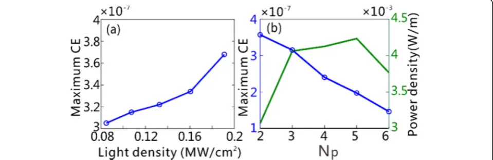
It is important to discuss the factors that affect the THG CE, which is key to evaluate the device perform-ance of a THG wavelength converter. For a THG process, one always expects to achieve the largest CE with a relatively small pump power. Previous studies demonstrated that, increasing the local field intensity in the third-order nonlinear materials yields a remarkable improvement of the CE of THG with a significantly re-duced pump power [3,4, 7]. Figure 6a shows the influ-ence of the power density of incident light waves on the maximum CE in the GSPWs, which is increased with the power density. Note that the maximum CE reaches
up to 3.68 × 10⁻⁷ even if the power density of incident light waves is as low as 0.19 MW/cm2, which is 6–7 or-ders of magnitude smaller than those within the same spectral band [22,23]. We show in Fig.6b that the used number of grating period, Np, affects the CE in the GSPWs as well. When Np is increased, a reducing por-tion of the THF GPs generated in the center of the grat-ing reaches the GSPWs because of the enhanced propagation loss induced by graphene absorption. Nevertheless, the input power, associated with Np, pre-sents linear enhancement. Therefore, the maximum CE of the THF GPs decreases with the increased Np. We emphasize here that the absolute output power density of THF GPs should be more meaningful to guide the de-sign of a THG wavelength converter for practical appli-cations, once the incident power density is fixed. Although the maximum CE of the THF GPs lies atNp= 2 in our case, the output power density of THG approxi-mates the maximum when Np≥3 (Fig. 6b). Therefore, we have employed 3 periods of grating for the demon-stration of the generation of THF GPs in the GSPWs. For future experimental implementation with the current design, the area of input FF source exceeds the grating region and is kept constant when generating THF GP with different grating numbers. In this case, the CE should be written as
CE¼
Z
PTHFz dz=PFFS ð9Þ
where the area of the FF source,S, is constant. Thus, the output power density will be proportional to the CE, and hence, one must properly select the optimal grating number to maximize the output power density of THF GP.
The physical characteristics of graphene may also affect the device performance of THF GPs once the
Fig. 6aThe maximum CE of THG as a function of the incident power density forNp= 3.bThe maximum CE and the maximum output power
[image:7.595.59.539.547.703.2]studied structure shown in Fig. 5a is ready. The Fermi energy, μc, and the number of graphene layers will sig-nificantly change the resonance wavelength of FF GPs (Fig.2f, i) and therefore affect the generation wavelength of THF GPs as well. In contrast, the τ, associated with the carrier mobility μ, barely influences the resonance wavelength of FF GPs as well as the generation wave-length of THF GPs (Fig. 2c). However, the propagation loss of FF GPs and THF GPs can be reduced by the use of a much larger τ (Fig. 2b), which thus notably in-creases the CE of THF GPs. Considering that a car-rier mobility of μ> 10 m2V−1s−1 (τ> 1.5 ps) is achievable in the experiment [32], our simulation re-sults (τ= 0.5 ps) shown in (Figs. 3, 4, 5 and 6) can conservatively present the device performance of the THF GP generator in Fig. 5a.
Finally, it is worth discussing the influences of surface roughness of graphene sheets on the device perform-ance. The surface roughness of graphene could poten-tially scatter plasmon, and hence, the plasmon loss will be enhanced [34]. The proposed THF GP generator shown in Fig. 5 can be fabricated based on the current micro/nano fabrication technology. One can first spin a 270-nm-thick polymethyl methacrylate (PMMA) onto the silicon substrate. The PMMA layer is developed with MIKE\IPA after a subsequent electron-beam lithography process. After that, a 60-nm-thick Cr layer is deposited on the resist with electron-beam evaporation deposition method. The silicon grating substrate can be formed with etching techniques such as inductively coupled plasma machine. Followed by wet etching method, the residual Cr layer is removed by wet etching method. At last, the graphene sheets are transferred onto the silicon grating to form the final structure shown in Fig.5.
Conclusion
We have numerically demonstrated the generation of the THF GPs in a graphene sheet on silicon gratings with the normal-incidence plane waves in mid- and far-IR regions. It was shown that THF GPs are gener-ated and transmitted on the graphene surface, and the CE is dramatically enhanced due to the signifi-cantly increased field intensity of the excited FF GPs in combination of the large third-order nonlinear sus-ceptibility of graphene. The generated THF GPs can be conveniently coupled to a GSPW, which greatly fa-cilitates the integration of the graphene-based wave-length converter on a silicon platform. Our proposal can stimulate making graphene-based light sources for mid- and far-infrared photonics on a silicon plat-form and hence broaden the functionalities of silicon photonics, such as signal processing, spectroscopy, and sensing.
Abbreviations
CE:Conversion efficiency; CW: Continuous wave; FDTD: Finite difference time domain; FF: Fundamental frequency; GP: Graphene plasmon;
GSPW: Graphene-silicon plasmon waveguide; GSSDG: Graphene sheets sustained by dielectric grating; PMMA: Polymethyl methacrylate; THF: Third-harmonic frequency; THG: Third-Third-harmonic generation
Acknowledgements Not applicable
Funding
National Natural Science Foundation of China (grant nos. 11474116 and 11674118) and State Key Laboratory of Advanced Technology for Materials Synthesis and Processing (Wuhan University of Technology).
Availability of Data and Materials
The datasets generated during and/or analyzed during the current study are available from the corresponding authors on reasonable request.
Authors’Contributions
JHL carried out the simulation under LC’s guidance, while TZ provided valuable discussion. JHL and LC wrote the manuscript. All authors read and approved the final manuscript.
Authors’Information Not applicable
Competing Interests
The authors declare that they have no competing interests.
Publisher’s Note
Springer Nature remains neutral with regard to jurisdictional claims in published maps and institutional affiliations.
Author details
1Wuhan National Laboratory for Optoelectronics, Huazhong University of
Science and Technology, Wuhan 430074, China.2State Key Laboratory of Information Photonics and Optical Communications, Beijing University of Posts and Telecommunications, Beijing 100876, China.
Received: 3 July 2018 Accepted: 12 October 2018
References
1. Zhu SN, Zhu YY, Ming NB (1997) Quasi-phase-matched third-harmonic generation in a quasi-periodic optical superlattice. Science 278:843–846 2. Raghunathan V, Borlaug D, Rice RR, Jalali B (2007) Demonstration of a
mid-infrared silicon Raman amplifier. Opt Express 15:14355–14362
3. Monat C, Grillet C, Corcoran B, Moss DJ, Eggleton BJ, White TP et al (2010) Investigation of phase matching for third-harmonic generation in silicon slow light photonic crystal waveguides using Fourier optics. Opt Express 18: 6831–6840
4. Corcoran B, Monat C, Grillet C, Moss DJ, Eggleton BJ, White T et al (2009) Green light emission in silicon through slow-light enhanced third-harmonic generation in photonic-crystal waveguides. Nat photon. 3:206–210 5. Monat C, Grillet C, Collins M, Clark A, Schroeder J, Xiong C et al (2014)
Integrated optical auto-correlator based on third-harmonic generation in a silicon photonic crystal waveguide. Nat Commun 5:3246
6. Carmon T, Vahala KJ (2007) Visible continuous emission from a silica microphotonic device by third-harmonic generation. Nat Phys 3:430–435 7. Sederberg S, Elezzabi A (2015) Coherent visible-light-generation
enhancement in silicon-based nanoplasmonic waveguides via third-harmonic conversion. Phys Rev Lett 114:227401
8. Li G, Li T, Liu H, Li K, Wang S, Zhu S et al (2011) Spectral analysis of enhanced third harmonic generation from plasmonic excitations. Appl Phys Lett 98:261909
10. Wu T, Sun Y, Shao X, Shum PP, Huang T (2014) Efficient phase-matched third harmonic generation in an asymmetric plasmonic slot waveguide. Opt Express 22:18612–18624
11. Soref R (2010) Mid-infrared photonics in silicon and germanium. Nat photon 4:495–497
12. Gao W, Shi G, Jin Z, Shu J, Zhang Q, Vajtai R et al (2013) Excitation and active control of propagating surface plasmon polaritons in graphene. Nano Lett 13:3698–3702
13. Nasari H, Abrishamian MS (2015) Quasi-phase matching for efficient long-range plasmonic third-harmonic generation via graphene. Opt Lett 40: 5510–5513
14. Hendry E, Hale PJ, Moger J, Savchenko A, Mikhailov S (2010) Coherent nonlinear optical response of graphene. Phys Rev Lett 105:097401 15. Gu T, Petrone N, McMillan JF, van der Zande A, Yu M, Lo GQ et al (2012)
Regenerative oscillation and four-wave mixing in graphene optoelectronics. Nat Photon 6:554–559
16. Wright A, Xu X, Cao J, Zhang C (2009) Strong nonlinear optical response of graphene in the terahertz regime. Appl Phys Lett 95:072101
17. Mikhailov S, Ziegler K (2008) Nonlinear electromagnetic response of graphene: frequency multiplication and the self-consistent-field effects. J Phys Condens Matter 20:384204
18. Nasari H, Abrishamian MS (2016) Electrically tunable, plasmon resonance enhanced, terahertz third harmonic generation via graphene. RSC Adv 6: 50190–50200
19. Ooi KJ, Cheng J, Sipe J, Ang L, Tan DT (2016) Ultrafast, broadband, and configurable midinfrared all-optical switching in nonlinear graphene plasmonic waveguides. APL Photonics 1:046101
20. Guo J, Jiang L, Jia Y, Dai X, Xiang Y, Fan D (2017) Low threshold optical bistability in one-dimensional gratings based on graphene plasmonics. Opt Express 25:5972–5981
21. Ahn KJ, Rotermund F (2017) Terahertz optical bistability of graphene in thin layers of dielectrics. Opt Express 25:8484
22. Liu C, Nakajima T, Sakka T, Ohgaki H (2008) Above-threshold ionization and high-order harmonic generation by mid-infrared and far-infrared laser pulses. Phys Rev A 77:043411
23. Chin AH, Calderón OG, Kono J (2001) Extreme midinfrared nonlinear optics in semiconductors. Phys Rev Lett 86:3292
24. Yan H, Li X, Chandra B, Tulevski G, Wu Y, Freitag M et al (2012) Tunable infrared plasmonic devices using graphene/insulator stacks. Nat Nanotechnol 7:330–334
25. Vakil A, Engheta N (2011) Transformation optics using graphene. Science 332:1291–1294
26. Hao R, Jin J, Wei X, Jin X, Zhang X, Li E (2014) Recent developments in graphene-based optical modulators. Front Optoelectron 7:277–292 27. Hao R, Du W, Chen H, Jin X, Yang L, Li E (2013) Ultra-compact optical
modulator by graphene induced electro-refraction effect. Appl Phys Lett 103:061116
28. Zhou X, Zhang T, Yin X, Chen L, Li X (2017) Dynamically tunable electromagnetically induced transparency in graphene-based coupled micro-ring resonators. IEEE Photon J 9:1–9
29. Jablan M, Buljan H, SoljačićM (2009) Plasmonics in graphene at infrared frequencies. Phys Rev B 80:245435
30. Zhu X, Yan W, Jepsen PU, Hansen O, Mortensen NA, Xiao S (2013) Experimental observation of plasmons in a graphene monolayer resting on a two-dimensional subwavelength silicon grating. Appl Phys Lett 102:131101 31. Palik E (1998) Handbook of optical constants of solids. Academic, New York 32. Bolotin KI, Sikes KJ, Jiang Z, Klima M, Fudenberg G, Hone J et al (2008)
Ultrahigh electron mobility in suspended graphene. Solid State Commun 146:351–355

![Fig. 2 The real [Re(1 nm.neff)] and imaginary [Im(neff)] parts of the effective index, and absorption versus wavelength with different values of μc, τ, and dg](https://thumb-us.123doks.com/thumbv2/123dok_us/8844891.932475/4.595.57.540.88.527/imaginary-effective-index-absorption-versus-wavelength-different-values.webp)