www.arpnjournals.com
POWER OPTIMIZATION OF SEMICONDUCTOR LASER DRIVER USING
VOLTAGE SCALING TECHNIQUE
Bhagwan Das1, M.F.L Abdullah1, Mohd Shah Nor Shahida1, Qadir Bakhsh1, Bishwajeet Pandey2
1Faculty of Electrical and Electronic Engineering, Universiti Tun Hussein Onn Malaysia (UTHM), Malaysia. 2Chitkara University Research and Innovation Network, Punjab, India
E-Mail: [email protected]
ABSTRACT
In this paper, green hybrid silicon semiconductor (HSS) laser driver is designed using voltage scaling techniques. Voltage scaling is very popular approach for reducing total power of integrated circuits. The HSS laser driver is designed using current mode logic (CML) technique, which is widely used technique for designing optical components. CML technique provides the strength to the laser driver for high frequencies mid-range infrared range. The HSS laser driver firstly, is developed in Matlab that consume very high power. After that, the HSS laser driver design is implemented on FPGA virtex-6 family, package FF784, XC6VCX75T device at speed of -2 using voltage scaling technique. The HSS laser driver is operated at different mid infrared range frequencies on Matlab based model and FPGA model. It is concluded that using voltage scale technique on FPGA, power optimization is performed for the HSS laser driver. In results for different mid-range infrared frequencies more than 95% power is saved by comparing the power consumption of Matlab based model and power-optimized model using voltage scaling on FPGA. This energy efficient design of semiconductor laser can be integrated with other optical components to make optical communication system green.
Key words: Current mode logic Field Programming Gate Arrays HSS Laser driver Power reduction Voltage scaling
INTRODUCTION
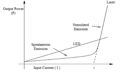
LED and Laser are two main optical sources but lasers are preferred due to its exceptional size, spectral region of procedure, high efficiency. Figure 1 describes the P-I curve for laser and LED operation, if the current value “I” is less than an edge value “i”, the light power is minor and the device works as LED by spontaneous emission. When “I” is greater than “i”, stimulated emission dominantly produce the high gradient efficient output as laser (Dawson et al., 2001). Laser operation have led to histrionic developments in high-speed optical communication systems (Seeds, 2014). In the beginning, the designers intended to improve the laser onset current, quantum productivity, light versus current characteristic, operation at high optical power, and long-term reliability (Elliott, 2014). The power consumption of laser and its related consequences considered as the secondary (Elliott, 2014). Presently, the power consumption and its reduction at high frequency is considered as important parameter like other, that has to be resolved before its physical realization (Butts & Sohi, 2000). There are many types of lasers are available in medical, industrial for research and commercial uses (Scruby & Drain, 1990). Lasers are often designated by the lasing medium type such as solid state, gas, excimer, dye, or semiconductor (Ganeev, 2014). Semiconductor lasers are widely utilized for electronic devices. Semiconductor lasers are also classified in different types depend upon active region and operation wavelength (Ganeev, 2014). In this research, the authors have used the Hybrid Silicon Semiconductor (HSS) laser that operates at Mid-infrared range (300 GHz to 30 THz) suitable for integrated optical communication systems (Liang & Bowers, 2010). Several techniques have been utilized to control the hysterical output of laser using laser driver, thermopile, optical sensors, laser calibration and others in (Tait et al., 2014). Among these techniques, the laser driver
[image:1.612.335.527.574.696.2]is preferred when laser power need to be control in terms of change in temperature, power, and frequency and with respect to other parameters (Krupke, 1989). Laser driver works as a switch that respond over an input signal modulated by the data pulses (Banu et al., 1991). Laser drivers are considered as current switch because it produces the output as a function of current instead of voltage as shown in Figure 1. The laser driver provides many benefits to be interfaced with laser such as it controls the fluctuation in the temperature that cause large current variations, controls the leakage current which produce the thermal excretion and others (Banu et al., 1991). Moreover, laser driver also performs high speed switching for laser and control the intensity of the transmitted signal before transferring to additional devices (Banu et al., 1991). Furthermore, these benefits still are not enough to provide the energy efficient output for the laser at high frequency operation of THz additional techniques need to be used for power efficient output must be used (Banu et al., 1991).
Figure 1: The P-I curve for LED and Laser (Dawson et al., 2001)
bandwidth using GaAs and InP (Xu, J., 2015). These laser drivers are used in local area network (LAN), metropolitan area network (MAN), Fiber take to home (FTTH) and consume more than 50 W for Mid range operation of HSS laser driver (Yoneki et al., 2015). However, it is investigated recently, that power consumption of the high frequency electronic devices can be compensated by designing the devices using FPGA accompanied with additional technique such as thermal scaling and etc. (Lakka etal., 2014).
It is quite hazardous, when HSS laser is directly interfaced with the optical system ahead at mid range infrared range. The existing laser driver are not capable enough to produce the energy efficient output. When laser driver is operated at above 500 GHz, the power consumption is increased drastically. At 10 THz, the power consumption is increased up to 95% (Seeds et al., 2015). This increment in power may destroy the device forever. The experimental procedure for designing the energy efficient laser is costly. In this work, power optimization is performed for HSS laser driver using voltage-scaling technique on FPGA. The paper is organized by discussing the background of the study and problem statement related with study in introduction part. Followed by basic concept of FPGA and voltage scaling technique used to address solution the problem. Later on methodology is discussed for power optimization of HSS laser driver using voltage-scaling technique on FPGA. Finally, results and discussion are S.
Field Programming Gate Array (FPGA)
The FPGA is standard platform that program the features and functions with hardware reconfiguration for specific application even after the product has been installed (Brown et al., 2012). Today, FPGA consist of various configurable systems, embedded RAM, high-speed transceivers, high speed I/Os, logic functions and routing. FPGA provides many advantages to design the energy efficient system (Brown et al., 2012). For example, ambient temperature scaling technique has been used to design thermal aware frame buffer thermal efficient FIR filter, Bengali Unicode reader, energy efficient ALU and room temperature aware fire sensor and others systems (Goswami & Pandey, 2014). The above system implemented in FPGA utilize the VLSI design for the system before its realization using Vhdl and Verilog (Alur, et al., 2015).
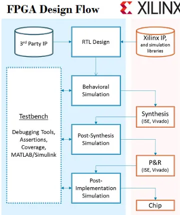
The design implementation using FPGA is explained in generic design flow in Figure 2 (Brown et al., 2012). In FPGA design, system is designed using third party softwares such as Matlab or others and is converted in Vhdl languages. After check syntax, the design is implemented in Xilinx and after verification process the design is transferred to chip. In this work, the HSS laser driver is designed on FPGA virtex-6 using voltage scaling technique. FPGA virtex-6 is consist of different voltage statues such as Core supply voltage (VCCINT), Auxiliary voltage (VCCAUX), Output driver supply voltage (VCCO), RAM block memory voltage (VCCBRAM), Reference voltage for IO standards (VREF), Key memory battery backup voltage (VCCBAT) (Kusse & Rabaey, 1998). Among these voltages the Auxiliary voltage (VCCAUX), Output driver supply voltage (VCCO) are played an important role in designing the power
[image:2.612.337.517.172.386.2]optimized for the specific system (Kusse & Rabaey, 1998). The designed system has its own operating voltage. If the voltage of the designed system is falling in the range of FPGA core voltages which is different for FPGA devices, system consume very low power (Brown et al., 2012). For this purpose, the voltage scaling is performed for core FPGA voltage to produce low power consumption for the designed system.
Figure 2: Generic FPGA Design flow (Brown et al., 2012)
Voltage Scaling
Voltage scaling technique reduces power consumption for different electronic devices by varying the voltage (Burd & Brodersen, 2000). The voltage scaling control the dynamic power and leakage currents of the devices. In the FPGA, voltage scaling is performed by varying the core voltage of the FPGA board. It is very difficult to find the exact value of voltage at which the device consumes less power (Burd & Brodersen, 2000). However, the scaling range should be in between base voltage and peak voltage of the FPGA. In FPGA, operating different devices at less than or equal to base voltage produce the halt condition for FPGA and at greater than or equal to peak voltage the device consume maximum power. Operating the designed system at peak voltage is not advisable. For the power optimization, the circuit should operate at the voltage that reduces power consumption as much as possible while maintaining reliable operation. The power consumption for the electronic devices is directly proportional to the square of the voltage applied to the circuit (Chandrakasan et al., 1992), as shown by equation (1) where C is the gate load capacitance (output capacitance),VD is the supply voltage and fc is the clock frequency. At high clock frequency the processor become slow down that slow down the execution rate.
c
D
f
CV
P
=
2*
(1)power consume by laser multiplied by pulse duration (t) of laser as shown in equation (2) (Ready, 2012) :
t
P
E
L=
L*
(2)The average power consume by laser is the product of pulse energy multiplied by repetition rate (Hz) of the laser as described in (Ready, 2012) equation (3):
Hz
E
P
L,Average=
L*
(3)The short pulse length of the laser produces high consumption power with comparatively low pulse energy (Ready, 2012).
METHODOLOGY
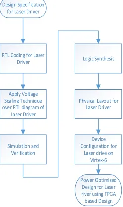
In this work, power consumption is reduced for HSS laser driver using voltage scaling technique. Figure 3 defines the methodology for designing the power optimization for laser driver.
Design Specification for Laser Driver
RTL Coding for Laser Driver
Apply Voltage Scaling Technique over RTL diagram of
Laser Driver
Simulation and Verification
Logic Synthesis
Physical Layout for Laser Driver
Device Configuration for
Laser drive on Virtex-6
[image:3.612.138.262.294.502.2]Power Optimized Design for Laser river using FPGA based Design
Figure 3: Power optimization of HSS laser driver.
Figure 3 states that HSS laser driver design is realized in Matlab using current mode logic. This design is converted in Xilinx design using FPGA generic flow design as discussed earlier. After that, RTL schematic coding is developed for the HSS laser driver. The voltage scaling technique is applied RTL schematic of the HSS laser driver. The simulation and verification is performed for the power-optimized design of the HSS laser driver. The successful verification of the HSS laser driver produces logic synthesis in which system is implemented on logic tabs. The Logic synthesis design of HSS laser driver design is converted in physical layout. The physical layout of the HSS laser driver is configure according to the FPGA devices. In this work, the physical layout is implemented over virtex-6. At the end, power optimized design is achieved for the HSS laser driver on FPGA.
The HSS laser driver using Current Mode Logic
The HSS laser driver is designed using current mode logic technique. The design is developed in Matlab.
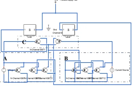
Current mode logic (CML) is point-to-point transmission for terminating the differential line (Current, 1994). CML is commonly used to interfaces fiber optic components. Using CML configuration a comparatively continuous current is regulated by eliminating unwanted common mode noisy signals. Secondly, if signals are symmetrical during propagation can reduced cross talk. Thirdly, their symmetrical behavior improves the wide band transmission. The laser driver is designed to modulate a laser with serial data pulses and provides DC bias (reference) current to the laser. Schematic diagram of designed laser driver circuit is shown in Figure 4 (Current, 1994). The CML based design can be implemented using N-Channel IGBT transsitor as mentioned in (Bose, 1992) (Khanna, 2004). The circuit consists of current mode logic (CML) with N-channel IGBT transistor arranged in two parallel logic network. The CML design of HSS laser driver contains the two N-channel IGBT transistor configurations. The parallel configuration of N-channel IGBT transistor shown by “A” in Figure 4 is producing the IGS, and other N-channel IGBT transistor network shown by “B” is producing the IDD, the difference
of these currents ∆ID is applied to “C” network, in which load and laser are connected in parallel configuration with N-channel IGBT transistor using equation (4). If the current drawn form the laser is equal to the difference of currents of network A and B. Then N-channel IGBT transistor (N1) is cut-off and direct output is delivered to load. If the laser current is greater than or less than the difference current of network A and B, then N-channel IGBT transistor (N2) is in cut-off, the average of laser current and difference current and ∆ID as shown in equation (5) is delivered to output load. The main advantage of this HSS laser driver circuit is that any fluctuation in the input of the laser is compensated by the two parallel networks A and B. This CML works as current switch between laser optical fiber. The lowest value of the input common-mode level, ISource,CM is attained, when current is about to fall in saturation when the tail current begins to operate in saturation. The CML level grasps its maximum value, ISource,Cmax when the transistors N1 and N2
are either at squeeze-off or at cutoff (Khanna, 2004):
] , 2 min[
)
(GS TH Source,CM DD SS TH DD
GS I I
I Load I I I I
I + + ≤ ≤ − + (4)
Where IGS is common mode overdrive current of N1 and N2. In generating the IGS, N3, N4 and N5 N-channel IGBT transistor are contributing, when working in linear or in saturation region, but in cut-off region the output is zero. In generating the IDD, N6, N7 and N8 N-channel IGBT transistor are contributing. Note when IGS is in saturation or in linear then IDD is zero or in cut-off region, when IGS is in cut-off region the IDD is maximum and works in linear region. The advantage of the using CML is that its large-signal behavior in response to a parallel configuration of N1 and N2 signals. Presumptuous that, CML is constrained
within the operating range detailed in equation (4), a small difference is produced between IGS and IDD, which is as follows (Khanna, 2004). In equation (5) ∆ID is called the laser driver current, which control the current of semiconductor laser. 2
4
2
1
SOURCE n SOURCE SOURCE n DD GS DI
I
I
I
I
I
=
=
∆
−
∆
∆
−µ
However, this laser driver still produces the unstably in the output when high frequency input is given. For this purpose, this HSS laser driver is realized in Xilinx for the power optimization of HSS laser river using voltage scaling. In the next, the laser driver is realized over FPGA as discussed in methodology.
Figure 4: HSS laser driver circuit using Current mode logic
Table 1 illustrates the parameters for HSS laser driver that includes operating voltage, current, frequency and others. When HSS laser driver is operated at mid-infrared range from 300 GHz to 30 THz, the power consumption is so high that practical realization of this design is not possible. When CML based HSS laser driver design is realized over 300 GHz, 900 GHz, 5 THz and 15 THz, the power consumption is recorded for this design was 25 W, 37 W, 46 W and 53 W respectively. To reduce the power consumption of the HSS laser driver, the design is realized on FPGA.
Table 1: Parameters for laser driver
Design Parameters Parameter’s specified range in SI
Operating laser frequency 10 GHz-20 THz
Operating wavelength of laser 1550 nm
Operating voltage 15 V
Operating current 15 mA
Operating laser beam width 280.5 nm
Operating laser bandwidth 46.5 GHz
Center wavelength 100000 nm
FPGA based design
There are different topologies and technologies available for realization of the circuit, such as electronic components, IC technology and System on Chip (SoC). In this work, CML based design of HSS laser driver is integrated on chip and final realization is performed using FPGA vertex-6 board (Palma et al., 2002). Table 2 shows, the design parameters for FPGA based realization of HSS laser driver. The parameters include the device model, programming method, ambient temperature of 25ºC. FPGA vertex-6 is used in this experiment, because High-density fabrication, Digital signal processing routine, and I/O standard facility, support high bandwidth up to 70 GHz, most robust serial interfaces with power: 50% lower than
previous generation (Palma et al., 2002). Xilinx FPGA vertex-6 module, supports different I/O standards. The characteristics of the I/O depends upon the FPGA having signaling principles. Some of them depends upon the reference voltage connected to the applicable pins of the FPGA, depending upon output buffers that need Vcco pins of the FPGA. In this work, LVCMOS IO standard is chosen for experiment because LVCMOS is the only IO standard, which has operates at 0.1-1 V voltage supply (Pandey etal., 2013).
Table 2: Parameters for FPGA based semiconductor laser driver
Parameters in FPGA design Parameter’s values for design
FPGA Vertex-6
HDL Verilog
Heat sink Medium profile Supply voltage 1.5 v Automatic FSM extraction Yes
FSM encoding algorithm Optimization algorithms Clock Buffer Clock of 1 GHz
IO standard LVCMOS
Ambient temperature 25ºC
Core FPGA Voltage 1.2 to 0.1 V
[image:4.612.71.291.148.291.2]In schematic design of HSS laser driver, two synchronized inputs with clock signal are included as reference input pulse stream. The clock signal is of 8 MHz, if it decreases below this range the CML logic is not triggered and circuit operates in cut-off region even the laser input is provided. If the clock signal increases beyond this value then CML triggered without even detecting the laser input and circuit operates in saturation. Therefore, for linear operation of semiconductor laser driver, it is necessary to fix the clock signal at this value for this CML configuration only. The clock signal may vary in other configuration of laser driver circuits.
Figure 5: Xilinx based design for HSS laser driver
The Xilinx based HSS laser driver design is tested over different frequencies and power consumption is reduced using voltage scaling technique. The total FPGA power consists of dynamic an leakage power. The voltage is scaled from 1.0 V (peak voltage) to 0.1V (base voltage) for virtex-6 FPGA. In the next section, the reduction in power consumption is achieved by varying the core voltage of FPGA from peak voltage to base voltage.
Power Consumption of Laser driver on FPGA
The laser power consumption and its measurement is already discussed above. Here it is demonstrated that how
B A
[image:4.612.327.532.498.589.2]power reduction is achieved using voltage scaling. Equation (1) describes the power of the current mode logic based laser driver. Equation (2) and (3) define the laser energy and average power consume by laser. Insert esquation (2) in (3)
Hz
t
P
P
L,Average=
L×
×
(6)Here P=PL, so equation (6) becomes
Hz
t
P
P
L,Average=
×
×
(7)Insert equation (1) in equation (7)
Hz
t
f
V
C
P
L,Average=
(
×
2×
c)
×
×
(8)Where fc is clock frequency and is equal to 1/T, put value in equation (8)
Hz
t
T
V
C
P
L,Average=
(
×
2×
1
)
×
×
(9)Simplify equation (9),
)
(
2,
Hz
T
t
V
C
P
LAverage=
×
×
×
(10)t/T is the constant ratio and termed Laser repetition ratio (LR), put in equation (10)
)
(
2,
C
V
L
Hz
P
LAverage=
×
×
R×
(11)Equation (11) elaborates that average laser power is only dependent on FPGA voltage only, the rest of the terms are constant and cannot be changed for the reliable operation of the laser.
Voltage Scaling of Semiconductor laser driver
The HSS laser driver is operated at 300 GHz, 900 GHz, 5 THz and 15 THz for different voltage statues. The power consumption is recorded for laser driver at different core voltages of FPGA.
The HSS laser driver power consumption at 1.0 V
[image:5.612.312.547.127.192.2]Table 3 shows, the power consumption of HSS laser driver at different operating frequencies of 300 GHz, 900 GHz, 5 THz and 15 THz at voltage of 1.0V. It is analyzed that for 300 GHz 24.7 W, for 900 GHz 36.5, for 5 THz 45.4 W and for 15 THz 52.7 W, power consumption is recorded. This Xilinx based power consumption is less than compared to Matlab model laser driver. Nevertheless, for the practical realization still the power consumption must be reduced.
Table 3: Power consumption in W at 1.0V
Frequency Total Power
300 GHz 24.7
900 GHz 36.5
5 THz 45.4
15 THz 52.7
The HSS laser driver power consumption at 0.9 V
When HSS laser driver is operated at similar frequencies, the power consumption is analyzed for 0.9 V of core FPGA voltage. Table 4 describes tht when voltage is
reduced from 1.0V to 0.9V, the power reduction is observed, 10% for 300 GHz, 5% for 900 GHz and 5 THz and 6% for 15 THz in comparison with power consumption ar 1.0V.
Table 4: Power consumption in W at 0.9V
Frequency Total Power
300 GHz 22.1
900 GHz 34.5
5 THz 43.1
15 THz 49.2
The HSS laser driver power consumption at 0.8 V
[image:5.612.315.547.314.374.2]Table 5 specifies the power consumption of HSS laser driver, when operated at 0.8V for all operating frequencies. If we compare the power values of 1.0V and 0.8V, the power reduction is recorded as as 21% for 300 GHz, 14% for 900 GHz, 12% for 5 THz and 12% for 15 THz. It is not necessarily the case that linear change in power reduction occur for all frequencies when voltage is reduced.
Table 5: Power consumption in W at 0.8 V
Frequency Total Power
300 GHz 19.3
900 GHz 31.2
5 THz 39.8
15 THz 46.2
The HSS laser driver power consumption at 0.7 V
[image:5.612.313.548.459.524.2]When semiconductor HSS laser driver is operated at 0.7 V, power reduction is achieved achieved, 34%, 30%, 29% and 28% for 300 GHz, 900 GHz, 5 THz and 15 THz respectively as shown in Table 6. The power comparison is made for 1.0 V and 0.8 V
Table 6: Power consumption in W at 0.7 V
Frequency Total Power
300 GHz 16.7
900 GHz 25.4
5 THz 32.1
15 THz 37.9
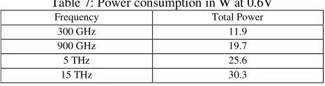
The HSS laser driver power consumption at 0.6 V
[image:5.612.65.298.627.691.2]Table 7 shows, the power consumption values for the HSS laser driver, when operating at the voltage of 0.6V. It is explored that power reduction is achieved for 300 GHZ, 900 GHz, 5 THz and 15 THz. If we compared the power consumption values of 1.0 V and 0.6 V, 51%, 46%, 43% and 42% power reduction is recorded 300 GHz, 900 GHz, 5 THz and 15 THz respectively.
Table 7: Power consumption in W at 0.6V
Frequency Total Power
300 GHz 11.9
900 GHz 19.7
5 THz 25.6
15 THz 30.3
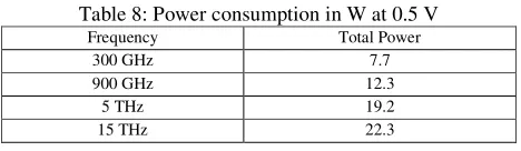
The HSS laser driver power consumption at 0.5 V
[image:5.612.314.547.633.695.2]THz 57% and for 15 THz 57%, when compared with 1.0V power consumption values.
Table 8: Power consumption in W at 0.5 V
Frequency Total Power
300 GHz 7.7
900 GHz 12.3
5 THz 19.2
15 THz 22.3
The HSS laser driver power consumption at 0.4 V
[image:6.612.328.544.195.322.2]In Table 9 investigation of power reduction is performed, when HSS laser driver is operated at 0.4V. The power reduction of 87%, 82%, 74% and 71% is recorded for 300 GHz, 500 GHz, 5 THz and 15 THz respectively.
Table 9: Power consumption in W at 0.4V
Frequency Total Power
300 GHz 3.1
900 GHz 6.3
5 THz 11.5
15 THz 15.2
The HSS laser driver power consumption at 0.3 V
[image:6.612.66.300.227.292.2]Table 10 evaluates the power reduction for 0.3V. The power reduction is recorded for different operating frequencies of 300 GHz, 900 GHz, 5 THz and 15 THz is 91%, 91%, 88% and 82% respectively.
Table 10 : Power consumption in W at 0.3V
Frequency Total Power
300 GHz 2.1
900 GHz 3.4
5 THz 5.1
15 THz 9.3
The HSS laser driver power consumption at 0.2 V
[image:6.612.66.301.363.426.2]When HSS laser driver is operated at 0.2V, the power reduction is examined conversely, to 1.0V. The power reduction is observed is of 96% for 300 GHz, 95% for 900 GHz, 94% for 5 THz and 93% for 15 THz as in Table 11.
Table 11 : Power consumption in W at 0.2V
Frequency Total Power
300 GHz 0.9
900 GHz 1.5
5 THz 2.7
15 THz 3.5
The HSS laser driver power consumption at 0.1 V
When HSS laser driver is operated at 0.1V, the highest amount of reduction is achieved on contrary, to 1.0V. The 0.1V is minimum values of voltage scaling, below this scaling can not be performed. At this stage, overall 98%, 97%, 97% and 96% power reduction is achieved for 300 GHz, 900GHz, 5 THz and 15 THz respectively, against the voltage scaling value of 1.0V as described in Table 12.
Table 12: Power consumption in W at 0.1V
Frequency Total Power
300 GHz 0.3
900 GHz 0.9
5 THz 1.2
15 THz 2.1
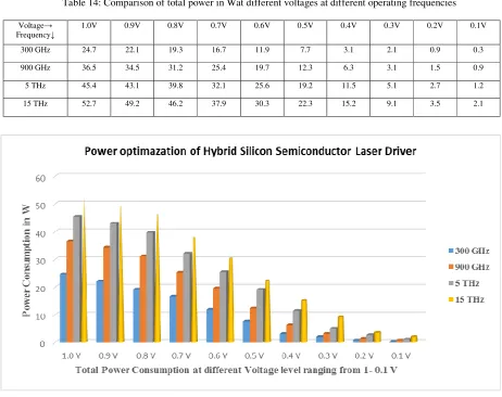
Results and Discussion
It is observed from Table 14 and Figure 6 that, at 3000 GHz, 900 GHz, 5 THz and 15 THz, power reduction is attained by voltage scaling from 1.0 V to 0.1 V for HSS laser driver. Table 13 describes the percentage of power saved for 300 GHz, 900 GHz, 5 THz and 15 THz by comparing the power consumption between Matlab based model and FPGA model of HSS laser driver.
Table 13: Power reduction in comparison with Matlab based model and FPGA based Model of Hybrid Silicon
Semiconductor Laser Driver Operating
Frequency
Power
Consumption
of Matlab
based Model
Power
consumption
using Voltage
Scaling on
FPGA
Power
Saved
300 GHz 25 0.3 98%
900 GHz 37 0.9 97%
5 THz 46 1.2 97%
15 THz 53 2.1 96%
Figure 6 states that high power consumption is recorded for laser driver when developed using Matlab (indicated using the brown line) but using voltage scale technique on FPGA (indicated using the yellow line), the power consumption is achieved. It is extracted that 98% power reduction is achieved for 500 GHz, similarly, for 900 GHz, 5 THz and 15 THz 97%, 97% and 96% power reduction is attained. Based upon these results it is suggested that voltage scaling is efficiently reducing the power consumption of the devices.
CONCLUSIONS
In this work, the power optimization for hybrid silicon semiconductor laser driver using voltage scaling technique is demonstrated. This design is realized in VHDL. It is concluded that, the energy efficient design for hybridnsemiconductor laser driver is achieved. Laser driver is realized on 40nm series of FPGA virtex-6. In future, there is possibility to apply these techniques on different optical components for making green optical communication. There is also a choice to redesign this laser driver using other latest FPGA series to increase the energy efficiency of hybrid silicon semiconductor laser driver. Furthermore, the energy efficient or power optimization of likely devices are very much helpful in designing the green communication system. Currenlty, the green communication are system in huge demand because high-speed communication consume enourmous power even the data traffic is off. The integration of the designed system with existing system also provide the less power consumption.
ACKNOWLEDGEMENT
[image:6.612.68.298.509.570.2]Table 14: Comparison of total power in Wat different voltages at different operating frequencies
Voltage→ Frequency↓
1.0V 0.9V 0.8V 0.7V 0.6V 0.5V 0.4V 0.3V 0.2V 0.1V
300 GHz 24.7 22.1 19.3 16.7 11.9 7.7 3.1 2.1 0.9 0.3
900 GHz 36.5 34.5 31.2 25.4 19.7 12.3 6.3 3.1 1.5 0.9
5 THz 45.4 43.1 39.8 32.1 25.6 19.2 11.5 5.1 2.7 1.2
[image:7.612.202.427.484.670.2]15 THz 52.7 49.2 46.2 37.9 30.3 22.3 15.2 9.1 3.5 2.1
Figure 6: Comparison of total power consumption in W for Matlab Model and Voltage Scaling based FPGA model of HSS Laser Driver at different voltages at different operating frequencies
REFERENCES
Alur, R., Henzinger, T. A., & Vardi, M. Y. (2015). Theory in practice for system design and verification. ACM Siglog News, 2(1), 46-51.
Banu, M., Jalali, B., Nottenburg, R., Humphrey, D., Montgomery, R., Hamm, R., & Panish, M. (1991). 10 Gbit/s bipolar laser driver. Electronics letters, 27(3), 278-280.
Bose, B. K. (1992). Recent advances in power electronics.
Power Electronics, IEEE Transactions on, 7(1), 2-16.
Brown, S. D., Francis, R. J., Rose, J., & Vranesic, Z. G. (2012). Field-programmable gate arrays (Vol. 180): Springer Science & Business Media.
Burd, T. D., & Brodersen, R. W. (2000). Design issues for dynamic voltage scaling. Paper presented at the Proceedings of the 2000 international symposium on Low power electronics and design.
Butts, J. A., & Sohi, G. S. (2000). A static power model for architects. Paper presented at the Proceedings of the 33rd annual ACM/IEEE international symposium on Microarchitecture.
Chandrakasan, A. P., Sheng, S., & Brodersen, R. W. (1992). Low-power CMOS digital design. IEICE Transactions on Electronics, 75(4), 371-382.
Current, K. W. (1994). Current-mode CMOS multiple-valued logic circuits. Solid-State Circuits, IEEE Journal of, 29(2), 95-107.
Dawson, W., Nakanishi-Ueda, T., Armstrong, D., Reitze, D., Samuelson, D., Hope, Koide, R. (2001). Local fundus response to blue (LED and laser) and infrared (LED and laser) sources. Experimental eye research, 73(1), 137-147.
Elliott, D. L. (2014). Ultraviolet laser technology and applications: Academic press.
Ganeev, R. A. (2014). Principles of Lasers and Laser-Surface Interactions Laser-Surface Interactions (pp. 1-21): Springer.
Goswami, K., & Pandey, B. (2014). LVCMOS Based Thermal Aware Energy Efficient Vedic Multiplier Design on FPGA. Paper presented at the Computational Intelligence and Communication Networks (CICN), 2014 International Conference on.
Khanna, V. K. (2004). Insulated gate bipolar transistor IGBT theory and design: John Wiley & Sons.
Krupke, W. F. (1989). Solid state laser driver for an ICF reactor. Fusion Technol.;(United States), 15 (CONF-881031-).
Kusse, E., & Rabaey, J. (1998). Low-energy embedded FPGA structures. Paper presented at the Low Power
Electronics and Design, 1998. Proceedings. 1998 International Symposium on.
Lakka, M., Koutroulis, E., & Dollas, A. (2014). Development of an FPGA-based SPWM generator for high switching frequency DC/AC inverters. Power Electronics, IEEE Transactions on, 29(1), 356-365.
Liang, D., & Bowers, J. E. (2010). Recent progress in lasers on silicon. Nature Photonics, 4(8), 511-517.
Palma, J. C., De Mello, A. V., Möller, L., Moraes, F., & Calazans, N. (2002). Core communication interface for FPGAs. Paper presented at the Integrated Circuits and Systems Design, 2002. Proceedings. 15th Symposium on.
Pandey, B., Yadav, J., Singh, Y. K., Kumar, R., & Patel, S. (2013). Energy efficient design and implementation of ALU on 40nm FPGA. Paper presented at the Energy Efficient Technologies for Sustainability (ICEETS), 2013 International Conference on.
Ready, J. (2012). Effects of high-power laser radiation: Elsevier.
Scruby, C. B., & Drain, L. E. (1990). Laser ultrasonics techniques and applications: CRC Press.
Seeds, A. J. (2014). TeraHertz photonics for communications. Paper presented at the Optical Fiber Communication Conference.
Seeds, A. J., Shams, H., Fice, M. J., & Renaud, C. C. (2015). TeraHertz Photonics for Wireless Communications.
Journal of Lightwave Technology, 33(3), 579-587.
Tait, A. N., Nahmias, M. A., Tian, Y., Shastri, B. J., & Prucnal, P. R. (2014). Photonic neuromorphic signal processing and computing Nanophotonic Information Physics (pp. 183-222): Springer.
Xu, J. (2015). Energy-efficient, high-speed integrated circuits for emerging computing and sensing applications.
University of Rochester.