Design of Bypassing Multipier with Different Adders
ManchalAhuja
1,Sakshi
2,*1Department of Electronics ,Thapar University, Patiala,147001, Punjab ,India 2Department of Electronics Faculty, Thapar University, Patiala,147001, Punjab ,India
*Corresponding Author: [email protected]
Copyright © 2014 Horizon Research Publishing All rights reserved.
Abstract
Multiplication is one of the essential operations in Digital Signal Processing (DSP) applications like Fast Fourier Transform (FFT), Digital filters etc. Multiplier is designed, considering the tradeoffs between low power and high speed. The bypassing multiplier is an improvement, over Braun multiplier which is one of the parallel array multiplier. The tradeoffs i.e. dynamic power and delay of the Bypassing multipliers can be reduced by using different adders. This paper presents a comparative study of 1-dimensional and 2-dimensional bypassing multipliers using different adders on basis of delay, area and power and for 4x4, 8x8 and 16x16 bits in FPGA Spartan – 3E using Xilinx 12.4 ISE and Synopsys respectively.Keywords
Bypassing, Delay, Power, Area, Comparison, Adders1. Introduction
Low power design has become a great concern in VLSI design in recent years. There exists a strong necessity to investigate techniques for lowering energy dissipation of devices, such as Digital Signal Processors(DSP). Digital multipliers are essential arithmetic blocks for many DSP applications: filtering, convolution, DCT, Fourier Transform, etc. It consumes almost 2/3 of the total power. As result optimizing the multipliers for energy is important.
In static CMOS, transition activity dominates the total energy dissipation due to charging and discharging of capacitors. Many prior digital multipliers were aimed at transition or switch reductions to reduce power dissipation as well. A
Leapfrog multiplier was proposed in [2] by using a hardware bypassing approach to avoid the redundant computations by disabling the adder units whose partial product becomes zero. Many low-power multiplier designs can be found in the literature. A straightforward approach is to design a multiplier that consumes less power [1] as well as less hardware. Another way is through modifying the structure of full adder at circuit level, depending on number of input[4]. Sung, Ciou, and Wang [3], proposed enhanced
efficiency by disabling most adders by introducing 2-dimensional bypassing. As adder is the last stage multiplication, so selecting adder is important part of the design. Efforts have been focused on comparative study and improvement of adder and multiplier designs [11].
For the multiplication of two unsigned n-bit numbers, the multiplicand A = an-1 an-2, . . . , a0 and the multiplier B = bn-1
bn-2, . . . , b0, the product P = P2n-1 P2n-2, . . . , P0, can be
represented as the following equation:
𝑃𝑃 = 𝐴𝐴𝐴𝐴 = �� 𝑎𝑎i2
𝑛𝑛−1
𝑖𝑖=0
i
� (∑𝑛𝑛−1
b
j2 j ) =𝑗𝑗 =0
𝑗𝑗=0𝑛𝑛−1𝑖𝑖=0𝑛𝑛−1𝑎𝑎i𝑏𝑏 j 2i+j (1)
where i and j are the number of bits in the multiplier and multiplicand, respectively. The multiplier output, for example: P1 is the result of addition of a1b0 anda0b1.
Multiplication is as shown in Figure 1.The terms generated are called partial products and these partial products are then added to get the final multiplier output.
Figure 1. How to multiply
[image:1.595.328.532.521.690.2](FAs) and 3 FAs in the last row construct a 3-bit ripple-carry adder. The advantage of the Braun array multiplier is its regular and compact structure, as it can be realized with parallel structure. The limitation is more hardware for braun multiplier that leads to more power consumption. The reduction of the power dissipation can also be achieved through the architectural modification via row bypassing or column bypassing or on the concept of the row and column bypassing, a low power 2-dimensional bypassing technique.
Figure 2. 4x4 Braun Multiplier[8]
2. Bypassing Multiplier
2.1. One Dimensional Bypassing
Consider a multiplier with multiplier bits b and multiplicand bits as a as shown in figure 3. A simple thought to improve performance is, as soon as bj was found to be zero, i. e., all partial products ai bj, 0≤ i ≤ n-1, are zero,
complete row is bypassed to avoid triggering those adding units in the row. Hence, two multiplexers are required in the adding unit to realize the bypassing operation. If the j-thbit of bis 0, hence the corresponding partial product is 0. To eliminate the redundant signal transitions, disable the adders whose partial product is zero, while shifting and bypassing the partial product of the previous adder rows to the next row of adders. Thus, the outputs from the (j-1)-th row is fed to the (j+1)-th row of CSAs without affecting the multiplication result.
For a column-bypassing multiplier [1],as shown in figure 4., the addition operations in the (i+1)th column can be
bypassed if the bit, ai, in the multiplicand is 0, i.e., all partial
products aibj, 0≤ j ≤ n-1, are zero. There are two advantages
to this approach. First, it eliminates the extra correcting circuit. Secondly, the modified FA is simpler than that used
[image:2.595.330.541.119.365.2]in the row-bypassing multiplier. Each modified FA in the CSA array is only attached by two tri-state buffers and one 2-to-1 multiplexer.
Figure 3. 4x4 Braun multiplier using Row Bypassing[4].
Figure 4. 4x4 Braun multiplier using column bypassing.[7].
2.2. Two Dimensional Bypassing
Prior designs considered reducing power either only with multiplicand or multiplier bits. Hence, to detect the bitwise nullity of the multiplicand in the vertical direction as well as the partial product in the horizontal direction in an array multiplier to remove the unnecessary operations taken place in the corresponding adding cells. The advantage of this design is less power consumption as less switching activity.
[image:2.595.88.271.194.426.2] [image:2.595.328.539.397.599.2]detects the bitwise nullity of the multiplicand bits, Yj’s, in
addition to the state of the multiplier, Xi’s. However, a
conflict appears when one adding cell, ACij, encounters a
scenario that Xi=Yj= 0.
For instance, assume i= 2, j = 1 and X2 = Y1 =0 in Figure. 5.
If the carry out of the adding cell AC12 is “1”, it should be
propagated to the carry in of AC31 and the nits carry out.
However, the carry bit will be lost if AC31 is bypassed due to
Y1 = 0. Consequently, an error is occurred, since the carry out
of AC31 will be zero. We, thus, propose to include bypass
logic (BL) in certain adding cells.
A. Adding Cell with and without bypass logic
According to the illustrative example, a simple rule is :If and only if Xi is not equal to “0” and the carry in is “1”, then
the adding cell, ACij, cannot be bypassed. Hence, an adding
cell with the bypass logic is proposed in Figure. 6. It is also represented by a gray box in Figure. 5. In order to save more bypass logic area, the adding cell AC30 can be further
simplified such that a single nand gate is used to replace the adding cell with bypass logic. It is obvious that not every adding cell needs th bypass logic. Given n = 4, it can be easily concluded that AC31 is the only unit with the necessity
of a bypass logic. By a similar induction, for any n x n multipliers, where n ≥ 4, all of the adding cells, ACij, where n
[image:3.595.335.517.83.386.2]− 1 ≥ i≥ 3 and n − 3 ≥ j ≥ 1, must contain the bypass logic to execute the correct multiplication. In other words, when n = 4, there is only one adding cell which must contain the bypass logic. The other cells are without bypass logic are ,as the structure of figure 7.
Figure 5. 4x4 Braun multiplier using row and column bypassing [3].
Therefore, the following rule is concluded. A total of (n − 3)2adding cells with bypass logic are required to constitute a
2-dimensional bypassing multiplier, ∀n >3.
Figure 6. Adding Cell with bypass logic[3]
Figure 7. Adding Cell without bypass logic.[3]
3. Adders
3.1. Ripple Carry Adder
Ripple carry adder can be designed by cascading full adder in series i.e. carry from previous full adder is connected as input carry for the next stage. In the case of a RCA, the critical path is from the least significant input x0 or y0 to the last sum bit sn. The major limitation of Ripple carry adder is that as the bit length goes on increases, delay also increases. Though the delay is large, but the area requirement is comparatively less as compared to other adders.
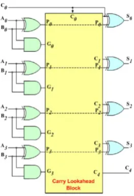
3.2. Carry Look Ahead Adder
Carry look ahead logic uses the concepts of generating and propagating carries. The generation and propogation can be expressed as
Gi=Ai.Bi and Pi=Ai+Bi
[image:3.595.73.282.440.705.2]Figure 8. Carry Look ahead Adder
3.3. Carry Select Adder
[image:4.595.109.241.75.268.2]The essence of the adder scheme is in the realization that we can add two numbers without waiting for the carry signal to be available. Simply, the numbers are added in two instances: one assuming Cin = 0 and the other assuming Cin = 1. The conditionally produced carry is selected through the multiplexer, as 2:1 multiplexer is seen in figure 9, which shows the block diagram of Carry select adder.
Figure 9. Schematic block diagram of 16-bit Carry select adder[11]
4. Experimental Results
The design of standard Row bypassing, Column bypassing and Row and Column Bypassing multiplier with different adders(Ripple carry, Carry look ahead, Carry select)for 4×4 ,8x8, 16x16 are simulated and synthesized using Verilog HDL. Table 1 shows comparison of different designs for maximum combinational delay, implemented in Xilinx ISE 12.4 targeting Spartan – 3E (xc3s500e-4fg320) FPGA. Using Design Vision Synopsys, the designs are synthesized for dynamic power and area as listed in Table 2 and 3. Figure 10 and Figure 11 are the graphical representation of Table 1 and 2 respectively. Figure 12 shows dynamic power for different adders of 8x8 multiplier with different bypassing techniques.
Table 1. Comparison of Delay of bypassing 8x8 r on Spartan – 3E (xc3s500e-4fg320).
Delay(ns) Ripple Carry Adder
Carry Look
ahead Adder Carry Select Adder
Row
Bypassing 23.252 22.618 18.374
Column
Bypassing 18.267 18.267 13.951
Row& Column
[image:4.595.311.553.231.303.2]Bypassing 25.646 23.268 20.467
Table 2. Comparison of dynamic Power a of different 8x8 multipliers on Spartan 3E (xc3s500e-4fg320)
. Power(mW) Ahead Adder Carry Look Carry Select Adder Ripple Carry Adder
Row Bypassing 0.7565 0.8977 0.775
Column Bypassing 0.8258 0.9174 0.8065
2-dimensional
[image:4.595.309.556.327.551.2]Bypassing 0.8060 0.8781 0.7312
Table 3. Comparison of Area of different 8x8 multipliers on Spartan 3E (xc3s500e-4fg320)
Area (Nand
gate) Ripple Carry Adder Ahead Adder Carry Look Carry Select Adder
Row Bypassing 6405.84 6246.347 9056.834
Column
Bypassing 7252.66 8196.35 9140.04
2-dimensional
[image:4.595.70.286.407.545.2]Bypassing 6089.809 6880.81 8986.925
Figure 10. The delay of 8x8 row bypassing, column bypassing and row and column bypassing, for different adders.
[image:4.595.350.516.586.729.2]Figure 12. The dynamic power of different adders for 8x8 row bypassing, column bypassing and row and column bypassing..
Figure 13. The areaof Ripple Carry, Carry look ahead, and Carry Select adder for 8x8 row bypassing.
Figure 14. The area of different adders for 8x8 row and column bypassing..
The area representation of ripple carry, carry look ahead, and carry select adder for one-dimensional row bypassing and 2-dimensional is shown in Figure 13 and Figure 14 respectively.
5. Conclusions
In this paper we have presented the implementation of bypassing multipliers with different adders in the Xilinx targeting Spartan – 3E (xc3s500e-4fg320) and Synopsys Design Vision. The use of different adders like carry look ahead adder (CLA), carry select adder apart from ripple carry adder(RCA) in the last stage helped to improve the efficiency in terms of delay and power.
The results show highest speed for column bypassing
when implemented with carry select adder compared with other bypassing multipliers. For area and dynamic power, two dimensional bypassing with ripple carry adder consumes least power and area as compared to row bypassing and column bypassing. Thus, we can conclude column bypassing with a carry select adder gives least delay and two dimensional bypassing techniques have lowest dynamic power consumption.
REFERENCES
[1] M. C. Wen, S. J. Wang and Y. M. Lin, “Low power parallel multiplier with column bypassing”, in Proc. IEEE International Symposium on Circuits and Systems, (ISCAS 2005), vol.2, pp.1638-1641, 2005.
[2] J. Ohban, V. G. Moshnyaga, K. Inoue, “Multiplier energy reduction through Bypassing of partial products”, in Proc. IEEE Asia-Pacific Conference on Circuits and Systems(APCCAS’02), vol.2, pp.13-17, 2002.
[3] G.N.Sung, Y.J.Ciou, C.C.Wang, “A power aware
2-dimensional bypassing multiplier using cell – based design flow”, in Proc. IEEE International Symposium on Circuits and Systems (ISCAS 2008), pp.3338 – 3341, May 2008. [4] Jin-Tai Yan and Zhi-Wei Chen, “Low-Power Multiplier
Design with Row and Column Bypassing,” in Proc. IEEE SOC Conference (SOCC 2009), pp.1227-230, June 2002. [5] K.C Kuo, C.W Chou, “Low power and high speed multiplier
design with row bypassing and parallel architecture”, Microelectronics Journal 41, pp. 639–650, 2010.
[6] B. Parhami, Computer Arithmetic: Algorithms and Hardware Designs, Oxford University Press, 2000.
[7] Jin-Tai Yan and Zhi-Wei Chen, "Low-cost low-power bypassing-based multiplier design", in Proc. IEEE International Symposium on Circuits and Systems (ISCAS 2010), pp.2338-2341,2010.
[8] Tushar V. More and Dr. R.V.Kshirsagar “Design of Low Power Column Bypass Multiplier using FPGA”, in Proc. IEEE International Conference on Electronics Computer Technology (ICECT) ,Vol.3, pp. 431 - 435, 2011.
[9] J. Selvakumar, V. Bhaskar “A low power multiplier architecture based on bypassing technique for digital filter”, in Proc..International Conference on Sustainable Energy and Intelligent Systems (SESICON 2011),pp. 260-263, June 2011 [10] Ugurdag , F.Keskin.O,TuncC,Temizkan.F,Fici,G,Dedeoglu, “RoCoCo: Row and Column Compression for high-performance multiplication on FPGAs”in Proc. 2011 9th East - West Design and Test Symposium,(EWDTS) ,pp. 839-844,2011.
[image:5.595.78.277.259.356.2] [image:5.595.82.274.395.486.2]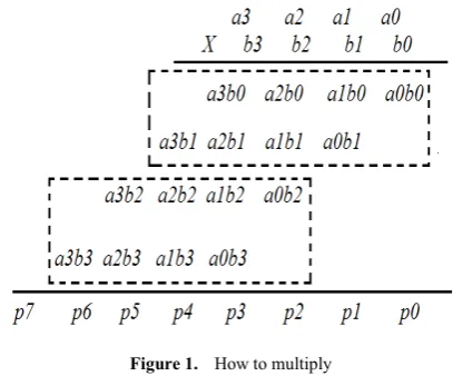
![Figure 3. 4x4 Braun multiplier using Row Bypassing[4].](https://thumb-us.123doks.com/thumbv2/123dok_us/8755497.892797/2.595.328.539.397.599/figure-x-braun-multiplier-using-row-bypassing.webp)
![Figure 5. 4x4 Braun multiplier using row and column bypassing [3].](https://thumb-us.123doks.com/thumbv2/123dok_us/8755497.892797/3.595.73.282.440.705/figure-x-braun-multiplier-using-row-column-bypassing.webp)