A Thesis by
RAJESH GARG
Submitted to the Office of Graduate Studies of Texas A&M University
in partial fulfillment of the requirements for the degree of MASTER OF SCIENCE
May 2006
A Thesis by
RAJESH GARG
Submitted to the Office of Graduate Studies of Texas A&M University
in partial fulfillment of the requirements for the degree of MASTER OF SCIENCE
Approved by:
Chair of Committee, Sunil P. Khatri Committee Members, Gwan Choi
Hong Liang Head of Department, C. Georghiades
May 2006
ABSTRACT
Generalized Buffering of Pass Transistor Logic (PTL) Stages Using Boolean Division and Don’t Cares. (May 2006)
Rajesh Garg, B.Tech., Indian Institute of Technology-Delhi Chair of Advisory Committee: Dr. Sunil P. Khatri
Pass Transistor Logic (PTL) is a well known approach for implementing digital cir-cuits. In order to handle larger designs and also to ensure that the total number of series devices in the resulting circuit is bounded, partitioned Reduced Ordered Binary Decision Diagrams (ROBDDs) can be used to generate the PTL circuit. The output signals of each partitioned block typically needs to be buffered. In this thesis, a new methodology is pre-sented to performgeneralizedbuffering of the outputs of PTL blocks. By performing the Boolean division of each PTL block using different gates in a library, we select the gate that results in the largest reduction in the height of the PTL block. In this manner, these gates serve the function of buffering the outputs of the PTL blocks, while also reducing the height and delay of the PTL block.
PTL synthesis with generalized buffering was implemented in two different ways. In the first approach, Boolean division was used to perform generalized buffering. In the sec-ond approach, compatible observability don’t cares (CODCs) were utilized in tandem with Boolean division to simplify the ROBDDs and to reduce the logic in PTL structure. Also CODCs were computed in two different manners: one using f ull simpli f y to compute complete CODCs and another using, approximate CODCs (ACODCs).
Over a number of examples, on an average, generalized buffering without CODCs results in a 24% reduction in delay, and a 3% improvement in circuit area, compared to a traditional buffered PTL implementation. When ACODCs were used, the delay was
reduced by 29%, and the total area was reduced by 5% compared to traditional buffering. With complete CODCs, the delay and area reduction compared to traditional buffering was 28% and 6% respectively. Therefore, results show that generalized buffering provides better implementation of the circuits than the traditional buffering method.
ACKNOWLEDGMENTS
I am very grateful to my advisor Dr. Sunil P. Khatri, for giving me this opportunity to work under him. Without his constant guidance, suggestions and encouragement, this work would not have been possible. I owe him gratitude for showing me this way of research. He has supported and encouraged me whenever I needed him and answered all my questions very openly. The informal group meetings organized by him have been a constant source of knowledge and inspiration. I also want to thank him for all the facilities and support he has given to me. Thanks a lot Dr. Khatri for everything.
I would also like to express my sincere acknowledgment to Nikhil Jayakumar and Kanupriya Gulati. Their constant support, valuable comments and guidance have helped me throughout the course of my Master’s study. They have also helped me in learning new things, given time to discuss the problems and has been a source of inspiration all along.
I would also like to thank my parents, brother and sister, who taught me the value of hard work by their own example. I would also like to share my moment of happiness with them. Without their encouragement and confidence in me, I would have never been able to pursue and complete my Master’s study.
Finally, I would like to thank all my friends, who directly and indirectly supported and helped me in completing this thesis.
TABLE OF CONTENTS CHAPTER Page I INTRODUCTION . . . 1 A. Previous Work . . . 4 B. Motivation . . . 8 C. Thesis Organization . . . 10 II BACKGROUND . . . 11
A. Pass Transistors Logic (PTL) . . . 11
B. Reduced Ordered Binary Decision Diagrams (ROBDD) . . . . 13
C. Compatible Observability Don’t Cares (CODCs) . . . 17
D. Conclusion . . . 21
III PARTITIONED ROBDDS . . . 22
A. Introduction . . . 22
B. Algorithm . . . 23
C. Conclusion . . . 24
IV PTL WITH GENERALIZED BUFFERING . . . 26
A. Introduction . . . 26
B. Boolean Division . . . 26
C. Generalized Buffering without CODCs . . . 27
1. ROBDD Division without CODCs . . . 30
D. Generalized Buffering with CODCs . . . 34
1. ROBDD Division with CODCs . . . 36
E. Conclusion . . . 38 V EXPERIMENTAL RESULTS . . . 39 A. Implementation Details . . . 39 B. Gate Library . . . 40 C. Delay . . . 40 D. Area . . . 43 E. Runtime . . . 45
F. Library Gates Utilized . . . 45
CHAPTER Page
VI CONCLUSIONS AND FUTURE WORK . . . 53
A. Conclusions . . . 53
B. Future Work . . . 54
REFERENCES . . . 56
LIST OF TABLES
TABLE Page
I Delay and active area of gate library . . . 41
II Delay Comparison of Generalized and Traditional Buffered PTL . . . 42
III Area Comparison of Generalized and Traditional Buffered PTL . . . 44
IV Run-time for PTL synthesis with generalized buffering . . . 46
V Number of MUXes and INV Utilized during Traditional and General-ized Buffering . . . 48
VI Number of Library Gates Utilized during Generalized Buffering with-out CODCs . . . 49
VII Number of Library Gates Utilized during Generalized Buffering with ACODCs. . . 50
VIII Number of Library Gates Utilized during Generalized Buffering with CODCs . . . 51
LIST OF FIGURES
FIGURE Page
1 ROBDD Node and its MUX based Implementation . . . 2
2 ROBDD and its PTL Implementation . . . 3
3 Static and PTL based implementation of AND Gate . . . 12
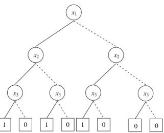
4 Shannon Cofactoring tree of logic function(x1+x2)·x3 . . . 14
5 OBDD of logic function(x1+x2)·x3 . . . 15
6 ROBDD for logic function(x1+x2)·x3 . . . 16
7 Nodeyk and its fanins . . . 19
8 Partitioned ROBDD of a Circuit (traditional buffering) . . . 24
9 Back-tracking during Division . . . 28
10 Dividing a Generalized Buffer into a PTL Structure . . . 31
CHAPTER I
INTRODUCTION
Static complementary metal oxide semiconductor (CMOS) has long been the circuit de-sign style of choice for digital Integrated Circuit (IC) dede-signers. Some the reasons for this are that static CMOS enables the design of reliable, scalable circuits and also due to the availability of a well-developed synthesis methodology for static CMOS. However, the switching capacitances in a static CMOS circuit can be fairly large. With the increasing demand for higher speed and low power, it has become necessary to look for alternative design styles which can offer better performance and power than static CMOS. The shrink-ing process feature sizes and increasshrink-ing transistor counts on a chip further emphasize this need. Many alternate circuit design styles have been proposed over the years, such as dynamic CMOS logic [1, 2], pass-transistor logic (PTL) [2], differential cascode voltage switch logic (DCVSL) [2], programmable logic arrays (PLAs) [2], etc.
Among these alternate circuit design styles, pass transistor logic (PTL) offers great promise. In contrast to dynamic logic, PTL is less susceptible to cross talk problems, which is a major issue in deep sub-micron technologies [3]. Several case studies [4, 5] have shown that PTL can implement most functions with fewer transistors than static CMOS or other styles. PTL circuits also have a physically dense structure and hence occupy less area. This reduces the overall capacitance, resulting in faster switching times and lower power.
PTL is a circuit implementation style that has typically been used for many specific circuit blocks like barrel shifters. Although PTL offers great benefits for such designs, there has been no widely accepted PTL design methodology that could be used to make PTL more broadly acceptable. There have however been several efforts at the research
level, to explore the promise of PTL.
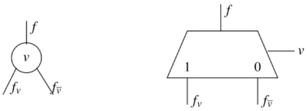
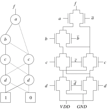
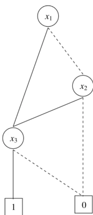
Synthesis approaches for PTL structures typically leverage the fact that there is a di-rect mapping between the Reduced Ordered Binary Decision Diagram (ROBDD) [4, 6] and the PTL implementation of a circuit. In fact, each ROBDD node can be mapped to a MUX (which can be implemented using NMOS or CMOS devices). Figure 1 illustrates the mapping between an an ROBDD node and a MUX whereas Figure 2 shows the mapping of ROBDD into PTL. In Figure 2 the solid line (dashed line) represents the positive (neg-ative) cofactor of an ROBDD node with respect to the variable of that node. For the PTL implementation of any function, there is an isomorphism between the connectivity of the ROBDD nodes of the function and the MUXes in the PTL implementation. This elegant and easy mapping between ROBDDs and PTL structures is not without attendant problems, however: 0 1 v f fv fv f fv fv v
Figure 1. ROBDD Node and its MUX based Implementation
• For one, in a bulk MOS implementation of any circuit, it is not practical to connect more than 4-5 devices in series, due to the phenomenon called body effect, which effectively increases the threshold voltageVT of most of the series-connected
MOS-FETs. This results in a slower design. Body effect is governed by the equation
VT =VT0+γpVsb (1.1)
1 0 a f b c d d c d c b a f a b c d d c VDD GND
Figure 2. ROBDD and its PTL Implementation
device at zero body bias,γis the body effect coefficient, andVsbis the source to bulk
voltage of the MOSFET. When several MOSFETs are connected in series in a PTL circuit, all but one of them is affected by body effect. For this reason, in practice, VLSI designers do not stack more than 4-5 devices in series.
This results in a problem for the traditional PTL implementations, which attempt to build monolithic ROBDDs. To solve this problem, we need to build ROBDDs in a partitioned [7] manner, such that if an intermediate ROBDD has a depth greater than 4 or 5, a new variable is created. In circuit terms, a buffer is implemented at the output of the new variable, ensuring that the circuit drive capability is regenerated every few levels in the final PTL design.
• The second problem is that ROBDDs, if build monolithically, can exhibit unpre-dictable memory explosion. This precludes the applicability of the PTL methodology for large designs, as long as the ROBDDs are build monolithically(since it is very hard to build monolithic ROBDDs of large functions). Again, the use of partitioned ROBDDs averts this problem.
In summary, partitioned ROBDD construction helps tackle both the above problems associated with PTL synthesis. In such a partitioned PTL design, the outputs of each PTL structure is buffered, to regenerate the electrical drive capability after every 4 or 5 levels.
The main goal of this thesis work is to implement a new PTL synthesis approach to perform efficient partitioned ROBDD based PTL synthesis. In principle, it still employs partitioned ROBDDs, however, the buffering between PTL stages is done using general-ized buffers. These could be arbitrary gates in the cell library. This is achieved by casting the problem of generalized buffering as an instance of Boolean division. In traditional par-titioned ROBDD based PTL synthesis, buffering is required after 4-5 levels as mentioned earlier. By using functionally complex library gates for the buffering logic, it is possible to significantly reduce the logic in the PTL structure which then results in a reduction of total circuit delay and area. A second goal of this thesis is to utilize Compatible Observabil-ity Don’t Cares (CODCs) during Boolean Division, to further reduce the logic in the PTL structures. The PTL synthesis approach with generalized buffering is implemented for both cases: one using CODCs and the other without CODCs. Also, to augment the applicability of the approach to industrial designs, approximate CODCs (ACODCs) are used as well.
A. Previous Work
There has been a significant amount of work in the area of pass transistor logic synthesis. In addition, there have been several reported design variations on the PTL circuit concept.
A good reference source for published work in this area is [8].The paper gives an overview of the state of the art in PTL technology. This paper covers PTL based circuit technologies, design and synthesis methodologies, applications and commercial use, etc. Given the gen-eral nature of the synthesis methodology which is presented in this thesis, the work of this thesis is orthogonal to the circuit issues and ideas that are discussed in the papers referred to in [8].
In [5], Yano et. al. present a scheme which takes a logic function described in hard-ware description language (HDL) format, and synthesize the corresponding PTL based circuit using a library of PTL cells, macrocells, etc. The scheme which was named as Lean Integration with Pass-Transistors (LEAP) uses a synthesis tool called “circuit inven-tor” which express the required logic function in ROBDD. Then the ROBDD is partitioned into smaller trees by inserting buffers at the nodes such that the height of the partitioned tree is less than the maximum height of the pass-transistor cell in the library. The library cells used [5] have a maximum height of two variables. After inserting the buffers, the partitioned tree is mapped using the PTL cells from the library. As monolithic ROBDDs are constructed (these can result in memory explosion), this tool can only be used for small circuits. This method uses inverters to buffer the signals between PTL cells.
The philosophy behind the work of Macchiarulo et. al. [9] is that while PTL based synthesis is well researched, layout and back-end tools for PTL are not found as readily. They describe a layout generator to help develop more complete tools for library free PTL design. The approach of Radhakrishnan et. al. [10] is motivated by the need to develop high density, low power, high performance circuits using PTL. The authors presents two synthesis approaches – a modified Karnaugh map [11] approach for small circuits, and a Quine-McCluskey [12, 13] based approach for larger designs. In [14], Cheung et. al. study regenerative pass transistor logic (RPL), a dual rail PTL family. Their interest stems from the compact area of these circuits. They implement an algorithm which tries to use
2-input RPL XOR logic gates and 2-input multiplexers as much as possible, to minimize the total number of transistors in the circuit. The algorithm also tries to minimize the serial connection of the pass-transistors to reducebodyeffect.
In [15], Hsiao et. al. present a layout and logic synthesis approach, with the input being a logic function, while the output is a PTL net-list, containing MUXes and inverters. After synthesizing the logic, the methodology adds inverters or buffers, in order to ensure that the longest series path of MUXes has a bounded depth. The work of Buch et.al. [3] builds ROBDDs [4, 6] in a partitioned manner [7], thereby avoiding the memory blow-up that often occurs while using ROBDDs. The resulting (small) ROBDDs are directly mapped to PTL structures, resulting in an efficient synthesis methodology. The downside of this approach is the absence of generalized buffering. The authors allude to performing PTL synthesis in a manner that maps some nodes to CMOS gates while others are mapped into PTL blocks. However, this leaves the designer little control of the depth of these sections. In contrast, the generalized buffering approach presented in this thesis guarantees a fixed bound on the depth of each PTL block, and also ensures just one level of generalized buffers between PTL blocks.
In [16], an approach using multilevel gates along with PTL and transmission gates is reported by Neves et. al., producing a regular and dense layout. The algorithm implemented by them first minimizes the logic function using a multi-level logic minimizer. Then the multi-level format is translated into a Directed Acyclic Graph (DAG). The DAG is then mapped into network of gates using the multi-level gates implemented in their library. Their approach also permits buffer inclusion. It can be viewed as an approach that combines synthesis and layout in the PTL design flow, and is orthogonal to the work presented in this thesis. The work of Pedron et. al. in the paper [17] reports synthesis algorithms for PTL. Minimization of circuit area is performed by using incomplete transmission gates. The results of synthesis using their tool PAVOS demonstrate good quality results when
compared with manually tuned PTL circuits.
In [18], Markovic et. al. present a PTL synthesis approach for Complementary Pass Transistor Logic (CPL), Dual Pass Transistor Logic (DPL) and Dual Voltage Logic (DVL). The approach for the logic synthesis is based on Karnaugh map coverage and circuit trans-formations. Finally, the work of Shelar et. al. [19] reports on a novel method to minimize power in a PTL structure. The authors transform the power minimization problem into a ROBDD decomposition problem and solve the latter using a max-flow min-cut approach. The results of the proposed algorithm in their paper achieves good power reduction as compared to previous low power PTL synthesis algorithms.
In [20], a mixed PTL-CMOS approach was presented by Lai et. al. The decomposi-tion process simply extracted unate variables from a sum-of-products (SOP) representadecomposi-tion of a function and recursively cofactored these variables (creating MUXes in the process) until unate leaves were reached. Unate leaves were realized using library gates alone. The weakness of this approach is that it starts with a SOP representation, limiting its effective-ness for large designs. Further, if a function is unate, then the entire circuit realization is purely standard-cell based. The work presented in this thesis works equally effectively for unate designs because it utilizes the partitioned ROBDD construction as the first step.
Another mixed PTL-CMOS approach was presented in [21]. The approach adopted by the authors is to construct the ROBDD of a logic function and then replace part of it with CMOS gates. The ROBDD nodes with one input connected to 0 or 1 terminal node are favored for replacement with CMOS gates. A cost function is used to finally decide upon the node replacement. The authors also control the ratio of the pass-transistors and CMOS gates by modifying a parameter of the cost function, and hence are able to do area-oriented, delay-oriented and power-oriented PTL-CMOS synthesis. However, the algorithm does not provide the user any control over the number of pass-transistors between two CMOS gates. Also, monolithic BDDs are used as a starting point for the approach, hence the algorithm
can only be applied to the smaller designs.
Most of the previous PTL logic synthesis approaches utilize monolithic ROBDDs which makes them inapplicable for larger designs. Although some of them have used par-titioned ROBDDs, they only use inverters for buffering signals between parpar-titioned blocks. However these approaches employ ad-hoc heuristics, yielding PTL structures which do not have control over the number of pass-transistors between two CMOS gates [21]. Other approaches [20], do not allow any control over the ratio of PTL blocks to standard cells. Our Boolean division based approach explores all possible ways to use arbitrary library cells. It also guarantees thatstatic CMOS gates are used only in the interface between PTL blocks, and that PTL blocks have bounded depth. Neither [21] nor [20] satisfy any of these properties. Also the methodology [20, 21] can only be applied to smaller designs because of their use of monolithic ROBDDs. Due to these problems associated with the previously proposed methods, there lies a significant scope for work in PTL based logic synthesis using CMOS gates. This thesis explores these opportunities.
B. Motivation
The shrinking feature size in recent VLSI designs and increasing demand for high speed and lower power makes it necessary to look for the circuit design styles other than Static CMOS, which have been predominantly used to implement VLSI circuits. Several differ-ent circuit design styles have been proposed such as dynamic CMOS logic, pass-transistor logic (PTL), differential cascode voltage switch logic (DCVSL), programmable logic ar-rays (PLAs), etc. Among these alternate circuit design styles, PTL circuit style possesses great potential. PTL can implement the logic function with fewer transistors than Static CMOS circuits. This reduction in transistors results in lower overall capacitance which increases design speed and decreases power consumption.
PTL approaches have been extensively researched earlier. However, there has been no widely accepted PTL design methodology. This has resulted in the application of PTL to specific circuit implementations. Many authors have tried to use PTL for general VLSI logic circuits but their approaches suffer from the problems as mentioned in the previous section. The key contribution of this thesis is to develop and implement a new PTL syn-thesis approach to perform efficient partitioned ROBDD based PTL synsyn-thesis. In principle, it still employs partitioned ROBDDs, however, the buffering between PTL stages is done usinggeneralized buffers. These could be arbitrary gates in a cell library. In traditional par-titioned ROBDD based PTL synthesis, buffering is required after 4-5 levels as mentioned earlier. By using functionally complex library gates for the buffering logic, it is possible to significantly reduce the logic in the PTL structure, which then results in a reduction of total circuit delay and area. The generalized buffering problem is solved using Boolean division. A second goal of this thesis is to utilize Compatible Observability Don’t Cares (CODCs) during Boolean division, to further reduce the logic in the PTL structures. The PTL synthesis approach with generalized buffering is implemented for both cases: one using CODCs and the other without CODCs. Finally, this thesis also uses approximate CODCs (ACODCs) during Boolean division, in order to extend the applicability of gener-alized buffering to indvidual designs.
The new PTL synthesis algorithm implemented in this thesis can synthesize combi-national logic circuits of arbitrary size. The approach of performing partitioned ROBDD construction using generalized buffers (library gates) to regenerate signal strengths across PTL structures is a novel contribution in the PTL synthesis world. The approach used for generalized buffering (using Boolean division), and the extension of this approach using CODCs and ACODCs is another novel contribution of this thesis.
C. Thesis Organization
The rest of this thesis is organized as follows: Chapter II provide some background in-formation which will be helpful in understanding the PTL based logic synthesis approach presented in this thesis. In Chapter III partitioned ROBDD construction is described. Chap-ter IV describes the new PTL synthesis algorithms proposed in this thesis. In ChapChap-ter V, experimental results are provided, comparing the new PTL synthesis approach (using gen-eralized buffering) with traditional partitioned ROBDD-based PTL design. Conclusions and future work are discussed in Chapter VI.
CHAPTER II
BACKGROUND
PTL possesses many advantages over static CMOS and other circuit styles. Among these properties of pass-transistors, the fact that there is direct mapping between an ROBDD and the PTL implementation of the corresponding function are mainly responsible for the potential that PTL possesses. To explain this further, it is useful to briefly describe pass transistors, ROBBDs, and compatible observability don’t cares (CODCs).
A. Pass Transistors Logic (PTL)
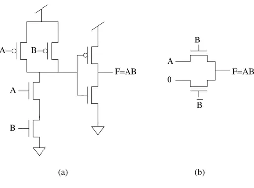
Pass transistor logic is a popular and widely used alternative to Static CMOS because of the advantages it possesses in terms of area and power as compared to CMOS, and other circuit styles [10, 3]. The pass transistor is simply an NMOS or PMOS device with inputs driving the gate as well as the source-drain terminals of the MOSFETS. This is in contrast with other circuit styles, which only allow inputs to drive the gate terminal. As an NMOS device is faster than PMOS transistor of the same size therefore, mostly NMOS transistors are used commonly to implement pass transistors in the PTL.
The main advantage of PTL is that it requires fewer transistors to implement a given logic function. Figure 3 shows the PTL and static CMOS implementation of a 2-input AND function. It can be seen that PTL based implementation requires 3 NMOS and 1 PMOS transistors (including the inverter required to invertB) to implement the AND gate whereas the corresponding implementation in static CMOS would require 6 transistors. The re-duction in the number of devices further decreases the overall capacitances and thereby increases the switching rate with a decrease in power.
The NMOS (PMOS) pass transistor is effective at passing a GND(VDD), but it is poor at passing aVDD(GND). Therefore, the output of a NMOS or PMOS pass-transistor
(a) A B F=AB F=AB B B A 0 B A (b)
Figure 3. Static and PTL based implementation of AND Gate
is not at the supply voltage. Also in a bulk MOS implementation of a circuit, the bulk terminal of all NMOS (PMOS) transistors are connected to GND (VDD). Due to this, when the transistors are connected in series, all but one of them experience an increase in its threshold voltage due tobody effect. The increase in threshold voltage is determined by the equation 1.1. The increase in threshold voltage increases the delay of the pass transistor (slows down the switching speed of the device). The NMOS transistor which is closer to GND in the series connected stack experiences a smaller increase in threshold voltage as compared to the transistor further away fromGND. Therefore, in practice it is not advisable to connect more than 4-5 transistors in series.
As mentioned in the last chapter, that there is a direct mapping between ROBDDs and PTL structures. Therefore, buffers have to be used after every 4-5 ROBDD nodes in series. In other words, partitioned ROBDDs with a depth less than 5 have to be built and
then mapped to PTL structures. ROBDDs are briefly discussed in next section whereas the implementation of the partitioned ROBDDs are described in detail in the next chapter.
B. Reduced Ordered Binary Decision Diagrams (ROBDD)
An ROBDD is a graphical way of representing a Boolean function. It can represent many logic functions compactly as compared with sum-of product (SOP). Moreover, many logic operations like tautology and complementation can be performed on ROBDDs in constant time. For a particular variable ordering , an ROBDD is a canonical form of representing a Boolean function. As the name suggests ROBDDs are a reduced form of binary decision diagram (BDDs) with a particular variable ordering. The reduction rules used are described in the sequel.
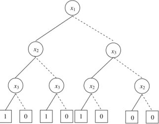
A BDD represents a Boolean function as a directed acyclic graph (DAG), with each nonterminal node labeled by a variable of the function. It is also referred to as a Shannon co-factoring tree, where each node performs the Shannon co-factoring of the Boolean func-tion represented by that node, with respect to the variable assigned to it. Figure 4 illustrates the BDD for the function(x1+x2)·x3. Each node has two outgoing edges, corresponding to the positive cofactor of the node function with respect to the node variable (shown as a solid line) or the negative cofactor of the node function with respect to the node variable (shown as a dashed line). The terminal nodes (shown as boxes) are labeled with 0 or 1, cor-responding to the possible function values. For any assignment to the function variables, the function value is determined by tracing a path from the root of the BDD to a terminal node following the appropriate positive or negative branch from each node. The number of vertices from the root to the leaves in the BDD is exponential in terms of number of variables in the logic function. Therefore, for functions with a large number of variables, BDDs might not be a good choice for representing the function. In general, the variable
ordering along different paths in the BDD can be different. 1 0 x3 x1 x2 0 0 0 x3 1 1 0 x2 x2 x3
Figure 4. Shannon Cofactoring tree of logic function(x1+x2)·x3
The graph in Figure 4 is transformed into an ordered BDDs (OBDDs) if we use a fixed variable ordering. Consider the variable to be orderx1<x2<x3. That is, every path from the root to a leaf encounters variables in the orderx1<x2<x3. The resulting OBDD is shown in Figure 5. If we further apply a set of reduction rules on the OBDD, we obtain an ROBDD for the function. The set of reduction rules are:
• Any node with two identical children is removed. • Two nodes with isomorphic BDDs are merged.
ROBDDs are a canonical form of representing a logic function for a particular vari-able ordering. Figure 6 shows the resulting ROBDD when the above mentioned reduction rules are applied to the graph shown in Figure 5. In this case as well, the number of nodes can be exponential in terms of the number of variables. However, the size of ROBDDs (i.e. number of nodes) depends upon the variable ordering. Therefore, variables must be ordered in a manner that minimizes the size of the ROBDD. The problem of comput-ing an optimum variable ordercomput-ing is a NP-Complete problem. However there are efficient
1 0 x3 1 0 x3 x1 x2 x2 x3 0 0 0 x3 1
Figure 5. OBDD of logic function(x1+x2)·x3
heuristics available that can choose an appropriate ordering of variables which results in the ROBDD of reasonable size. At the same time, there are functions that have polyno-mial sized multi-level representations while their ROBDDs are exponential for all input orderings. A multiplexer is an example of such a function.
The following ROBDD operations are used in the work presented in the thesis: • bdd and : This function returns the ROBDD which is the logical AND of the two
ROBDDs passed to the function.
• bdd or: This function returns the ROBDD which is the logical OR of the two ROB-DDs passed to the function.
• bdd xnor: This function returns the ROBDD which is the logical XNOR of the two ROBDDs passed to the function as a parameter.
• bdd compose: This function returns a ROBDD F0 with a variablev replaced by a ROBDDgin the original ROBDDF.
x1
x3
x2
0 1
Figure 6. ROBDD for logic function(x1+x2)·x3
the variables in the array “smoothing vars”. “smoothing vars” is an array of ROB-DDs, which are the single variable BDD formulas to be quantified.
Existential quantification of f with respect to a variable x is expressed as ∃xf = fx+ fx. Here fx represents the function f co-factored with respect to variable x.
Smoothing a set of variables is achieved by performing existential quantification, one variable at a time.
• bdd between : Returns a heuristically minimized BDD containing fmin, and
con-tained in fmax.
• bdd depth: Returns the depth of ROBDD i.e. the maximum number of nodes from the root vertex to any leaf.
C. Compatible Observability Don’t Cares (CODCs)
Technology independent logic optimization of a multi-level network is an important part of logic synthesis. During such optimization, one of the operations involves the computation of multi-level don’t cares of the circuit. These don’t cares can take the form of Satisfiability Don’t Cares (SDCs), Observability Don’t Cares (ODCs) or External Don’t Cares (XDCs). Of the different kinds of don’t cares, XDCs are specified with the network whereas SDCs and ODCs are computed. Consider a multi-level boolean network (η) in which every node has a Boolean function fi associated with it. Also, fi has a corresponding Boolean
variable yiassociated with it, such thatyi≡ fi. Suppose that the Boolean networkηhasn
primary inputs andmnodes. Then the SDCs are defined by the equation 2.1. SDCs simply convey that for each node in the network, the value of the node output (yj) cannot differ
from the value obtained after evaluating its boolean function (fj).
SDC=Σmj=1(yjfj+yjfj) (2.1) The Observability Don’t Care (ODC) of nodeyj (in a multi-level Boolean network)
with respect to outputzkis
ODCjk={x∈Bns.t. zk(x)|yj=0=zk(x)|yj=1} (2.2)
In other wordsODCjkis the set of minterms on the primary inputs for which the value
ofyjisnot observableatzk [22]. This can also be denoted as
ODCjk= (∂y∂zk j)
where
∂zk
∂zk
∂yj is also known as the Boolean Difference ofzkwith respect toyj.
Once a node function is changed by minimizing it against its ODCs (using Espresso [23]), the ODCs of the other nodes must be recomputed. To avoid re-computation of ODCs during optimization, Compatible Observability Don’t Cares (CODCs) [22] were developed. The CODC of a node is a subset of the ODC for that node. Unlike ODCs, CODCs have a prop-erty that one cansimultaneouslychange the function of all nodes in the network as long as each of the modified functions are contained in their respective CODCs. Compatibility is achieved by ordering the don’t care computation in a manner that if nodemiprecedes node
mj in the order, then node migets the most don’t cares. Also, while computing the don’t
cares ofmj, compatibility is maintained with the don’t cares already assigned to nodemi.
The computation of CODCs [22] in SIS [24] is performed in two phases.
• The first phase computes the CODC of a node using node operations. The resulting CODC is a function of arbitrary nodes in the network. However, we desire the sup-port of the CODC to be the supsup-port of the node itself. For this reason, we need a second phase in the computation to achieve this.
• In the second phase, image computation is performed to map the CODC points to the local fanin space of each node. This image computation uses BDDs.
In the first phase, the CODC computation for the networkηstarts from the primary outputs and proceeds towards primary inputs in a reverse topological order. The CODC at each primary output is initialized to the external don’t care (XDC) at that node.
The CODC at node yi (denoted as CODCiη) is found by using the CODC for each
fanout edge eik ofyi. This compatible don’t care of edgeeik is denoted byCODCikη. The
CODC foryiis obtained by intersecting the CODCs computed for its fanout edges.
Suppose, as shown in Figure 7, that we have a node with functionyk= fk, and ordered
... ... ... yk fk y1 y2 y3 yi−1 yi
Figure 7. Nodeykand its fanins
ofykas follows. CODCikη ≡(∂y∂fk 1+Cy1)...( ∂fk ∂yi−1+Cyi−1) ∂fk ∂yi +CODC η k (2.4)
Note that in the above computation, we assume thatCODCηk have already been com-puted. Also,Cyj is the consensus1operator. For the first input in the ordered list of fanins,
we haveCODC1ηk= (∂∂yfk
1) +CODC
η
k, indicating that this node obtains maximum flexibility.
The intuition behind the correctness of the computation of Equation 2.4 in general is that the new edge eik should have its don’t care condition as the conjunction of ∂∂yifk with the
condition that other inputs j<iare not insensitive to the inputyj(∂∂yfk
j), or are independent
ofyj (Cyj) indicating that the nodeiis free to use such terms independently of howyj was
simplified. Finally, the CODCs of the fanout nodeyk are also CODCs of the edgeeik. As
a result, the computation ofCODCikη using the formula above, performed in the specified order, results in the Compatible set of ODCs of the edgeseik. FromCODCikη, we compute
the CODC for nodei(CODCiη) as follows:
1Consensus operation on f with respect to a variableyis expressed asCyf = fyfy. Here fy represents the function f co-factored with respect to variabley.
CODCηi ≡
∏
k∈FOi
CODCikη (2.5)
The intuition of the above method of computing the CODC ofyi (CODCiη) based on
its edge CODCs (CODCikη) is thatCODCiηmust not be greater than anyCODCikη. Note also that all terms inCODCikη from Equation 2.4 exceptCODCkη have a support which is the support ofyk. However,CODCiη has a support which includes its fanout’s fanins, and in
general, we have to do an image computation to convert this CODC to a function which is on the support ofyi.
In the second phase, we perform this image computation. Using the ordering heuris-tics of [25], global BDDs at each node of the Boolean network are computed in terms of the primary inputs. BDDs are also built for each primary output in the external don’t care network using this same ordering. We next compute the CODC at yi in terms of primary
inputs, using a BDD based computation. This is done by substituting each literal of the CODC ofyiby its global BDD function (which was computed earlier). From this we find
all the points that are reachable in the local space of yi by a BDD based image
computa-tion. The functions used for image computation are the global functions at the fanins of yi. In most cases the number of primary outputs is much less than the number of primary
inputs; therefore the recursive image computation method [26] is used to do the compu-tation. However, this computation is highly memory intensive, since it is typically done using ROBDDs. As it is already mentioned earlier, ROBDDs can exhibit highly irregu-lar memory requirements, with unexpected blowup. As a result, the CODC computation, though very elegant in its conception, is typically not feasible for large circuits. In gen-eral, the computation is not robust for medium-sized circuits either. The work presented in this thesis is applicable for large circuits also therefore, an alternative way of computing
CODCs has to be employed.
In [27], the authors have presented a way of computing approximate compatible don’t cares (ACODCs). These don’t cares are approximation of CODCs. The ACODCs can be computed for larger designs and the time required and memory utilization for the ACODC computation is much less (both typically 30X lower) than the corresponding values for full CODC computation. At the same time, the literal count reduction obtained by ACODCs is typically about 80% of that obtained by full CODCs. To compute ACODCs for any noden, a smaller sub-network is extracted from the original network. The smaller network is a network rooted at the node of interest, up to a certain topological depth in the origi-nal network. Then the CODCs are computed for the smaller network. This can be done quite efficiently. The authors show that the don’t cares computed in this manner yields a literal count reduction which is about 80% of that obtained by complete CODCs. Hence, ACODCs will be used in this thesis work.
D. Conclusion
This chapter briefly dicuss the background information which will be required to under-stand this thesis. The next chapter will descibe the algorithm for create of partitioned ROBDDs.
CHAPTER III
PARTITIONED ROBDDS A. Introduction
Though PTL circuits possess many advantages over other circuit styles there are a couple of issues that need to be addressed. Firstly, due tobody effectin a practical PTL approach it is not advisable to connect more than 4-5 pass transistors in series. Secondly, since the PTL synthesis method uses ROBDDs, memory explosion can occur if ROBDDs are built monolithically. The first problem can be solved by inserting buffers after every 4-5 ROBDD nodes (pass-transistors). However, if monolithic ROBDD are used as the starting point for PTL synthesis (monolithic ROBDDs can have a size which is exponential in number of the inputs) then the advantage of PTL over other circuit styles will be lost in terms of area, power and delay. Therefore to avoid memory explosion, partitioned ROBDDs should be employed to construct the ROBDDs of the design. The use of partitioned ROBDDs also tackle the first problem, by buffering the output of every PTL structure.
Partitioned ROBDDs avoid the memory explosion which is possible when using mono-lithic ROBDD. The intuition behind this savings in ROBDD size is as follows: in gen-eral, when constructing the ROBDD of functionF =G1<op>G2, the size ofF is |F|, F =O(|G1||G2|)[4], where |G1|and|G2|are the sizes of the ROBDDs of G1 andG2 re-spectively. If the partitioned ROBDDs are built forF, then the aggregate size of ROBDDs will beO(|G1|+|G2|)[3]. Thus partitioned ROBDDs certainly reduce the aggregate size of the ROBDDs of the circuit. For this reason, partitioned ROBDDs allow us to construct the ROBDDs of large circuits when monolithic ROBDDs fail. The price to pay is that unlike monolithic ROBDD, partitioned ROBDDs are not canonical for a given variable ordering. However, this does not pose a problem in this thesis work, since this thesis deals with
gen-erating PTL circuits and not in manipulating ROBDD as a data structure. The algorithm for constructing partitioned ROBDDs is briefly discussed in the next section.
B. Algorithm
Consider a Boolean network η. First the network η is optimized and decomposed using 2-input gates and inverters only. Let the modified network be represented byη∗. Nowη∗is
sorted in a depth-first manner. The resulting array of nodes is sorted inlevelization1order, and placed into an array L. Thus the nodes ofη∗ are stored inAin topological order from
the inputs to the outputs.
Now a noden is fetched from array A in index order. The ROBDD f of n is built using the ntbdd node to bdd function. Let mbe the level of node n. Then the depth of the resulting node ROBDD f is compared with the maximum allowable depth of 5 (which maximum number of ROBDD nodes between the root and leaves). If the depth of f is less than 5 then we continue to create the ROBDD of other nodes in arrayA. However, if the depth of f is equal to 5 then the nodenis made a new variable. If the depth is greater than 5 then one of the fanins ofnis made a new variable. The fanin which is made a new variable is one whose topological level is one less than that ofn. Recall that any node can have at most two fanins. If both fanins have the same topological level, then the fanin node with maximum ROBDD depth is made as a new variable.
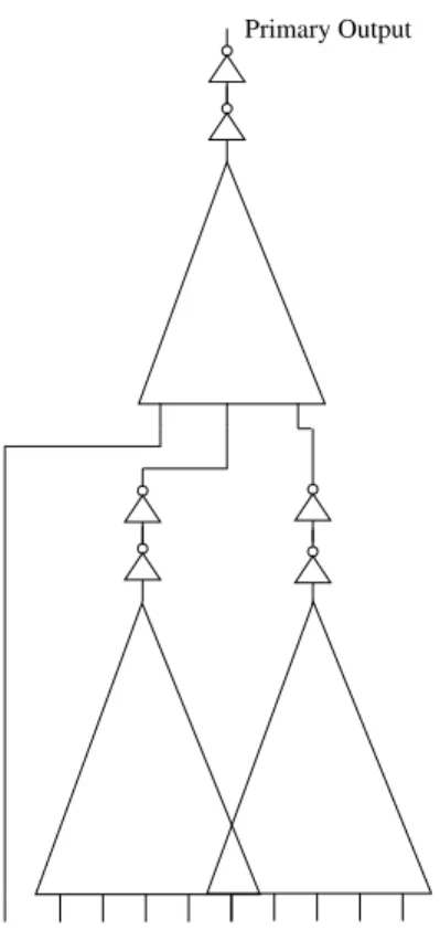
In this way, we can guarantee that no PTL structure will have a depth more than the maximum allowable depth of 5. Algorithm 1 summarizes the methodology of partitioned ROBDD construction. Figure 8 shows the resulting partitioned PTL implementation of a circuit with one primary output and 10 primary inputs. The triangles in the figure represent the partitioned ROBDDs whereas the top vertex of each triangle is a variable created during 1Primary inputs are assigned a level 0, and other nodes are assigned a level which is one
partitioned ROBDD construction. The top vertex of each triangle is also buffered as shown by the buffers (two back to back inverters) connected to each triangle’s vertex.
Primary Output
Primary Inputs
Figure 8. Partitioned ROBDD of a Circuit (traditional buffering)
C. Conclusion
Partitioned ROBDDs are very effective in the ROBDD construction of large circuits as compared with monolithic ROBDDs. They also help in PTL synthesis by allowing the resultant PTL implementation to have a bounded depth (thereby avoiding a delay increase due to body effect). The use of partitioned ROBDDs in PTL synthesis also avoids the memory explosions that is possible if monolithic ROBDDs are used. This avoids an area increase that would result if monolithic ROBDDs are used.
Algorithm 1Partitioned ROBDD Construction η= optimize network(η)
η∗= decompose network(η, 2)
A= dfs and levelize nodes(η∗)
i= 1
whilei≤size(A)do n= array fetch(A,i)
f = ntbdd node to bdd(node)
ifbdd depth(f)>5then
f anin= node fanin(n,level(n-1)) bdd create variable(f anin)
else ifbdd depth(f) == 5then bdd create variable(f) else continue end if end if end while
CHAPTER IV
PTL WITH GENERALIZED BUFFERING A. Introduction
Partitioned ROBBD (described in the last chapter) enable us to implement a PTL based circuit efficiently. However, this approached uses only inverters for buffering the signals between the partitioned PTL blocks and hence does not explore the advantage which gen-eralized buffering can offer. This thesis formulates a novel approach to do gengen-eralized buffering, by casting the problem as an instance of Boolean division. The Boolean division of a partitioned PTL block with complex library gates can significantly simplify the logic function of that PTL block. This results in the reduction of total circuit delay and area.
This chapter presents the key contribution of this thesis i.e. a new PTL synthesis methodology which uses generalized buffering between partitioned PTL blocks. The new PTL synthesis method is discussed for two cases: one with CODCs and the other with-out CODCs. In order to extend the applicability of the technique, the experiments were conducted using ACODCs as well. The next section introduces Boolean division. The fol-lowing two sections will present a PTL synthesis methodology for generalized buffering without using CODCs, and with CODCs.
B. Boolean Division
Boolean Division is extensively used in many logic optimization procedures like factoring, resubstitution, extraction, etc. Consider a completely specified Boolean function f which we want to divide by another completely specified Boolean functiong. Boolean division can be defined as:
gis said to be aBoolean factorof f if, g is a Boolean divisor of f, and, in addition r= /0, i.e., f =gh.
In this case,his called thequotientandris called the remainder. Note thathandr are not unique.
Theorem B.1 If f g6= /0, then g is a Boolean divisor of f .
Proof: If f g6= /0, we can write f = f g+f g
f =g(f+x) +f gwherex⊆g
which is of the form f =gh+r, whereh= f +xandr= f g.
C. Generalized Buffering without CODCs
The new PTL synthesis method described in this section does not use CODCs. Lets define thedepth of an ROBDD gas the maximum number of nodes in any traversal of g to its terminal nodes. Our method creates partitioned PTL structures with a maximum depth of 5 (this number can be arbitrary, though). This ensures that there are no more than 5 transistors in series, in any PTL block.
In order to implement generalized buffering, Boolean division will be used. Algorithm 2 describes the new PTL synthesis methodology which uses generalized buffers. Consider a boolean networkη. First the networkηis optimized and decomposed using 2-input gates and inverters only. Let the new network be referred to asη∗. Nowη∗is sorted in depth-first
manner. The resulting array of nodes is sorted inlevelizationorder, and placed into an array L.
In this approach, we first build ROBDDs of the nodes ofη, topologically from the inputs to the outputs by fetching the nodes from the arrayAin index order. Suppose we encounter a new nodenfor which we want to construct a ROBDD f. The ROBDD of each
of its fanins must have a depth of at most 4 ROBDD variables (assuming that the fanins are not partitioned ROBDD variables). When constructing the ROBDD f ofn, it can initially have at most 8 ROBDD variables (since any node in the original network can have at most 2 fanins). If the depth of f is less than 5 then we continue with creating the ROBDD of the other nodes in array A. However, if the depth of f is greater than or equal to 5 then we attempt to divide f with the gates in a library by calling the test division function. If the division is successful, then the depth of the ROBDD f will reduce . The detailed description of thetest divisionfunction is provided after the synthesis flow.
When we perform ROBDD construction, the maximum depth of the ROBDD of a nodenbefore division can be 8, as discussed earlier. The division routines systematically reduce this depth to below 5, by using one or more generalized buffers. If an ROBDD cannot be divided (and the resulting depth after division is greater than 5), then we back-track, and make one of the fanins of n a new variable. The fanin which is made a new variable is the one whose topological level is one less than that ofn. The reason for this is illustrated in Figure 9.
d e
c
b a
Figure 9. Back-tracking during Division
Consider nodea, at topological leveln. Suppose it has two faninscandd, with levels n−1 andn−2 respectively. Since partitioned ROBDD construction occurs in topological
Algorithm 2Pseudo Code for PTL synthesis using generalized buffers and without CODCs η= optimize network(η)
η∗= decompose network(η, p)
A= dfs and levelize nodes(η∗)
i= 1
whilei≤size(A)do n= array fetch(A,i)
f = ntbdd node to bdd(n)
ifbdd depth(f)≥5then
forg≡G∈Gate Librarydo f =test division(f,g,G) end for ifbdd depth(f)>5then back-track else bdd create variable(n) continue end if else continue end if end while
order from inputs to outputs, it is possible that nodeb(at leveln) has already been processed and divided. Its ROBDD therefore has a depth of less than 5 nodes. Now suppose the ROBDD depths of d and c are 4 each, and the ROBDD of a has depth 8. Suppose all divisions for nodeafail. In that case, we need to back-track and make eithercorda new variable. This would guarantee that a has a new depth 5. We select c(with level n−1) as the new variable since it is more likely that d (which is at a lower topological level) has more fanouts of level n orn−1. When c is made a new variable, all its fanouts are checked. If any of them has already been processed (such fanouts must have leveln), then their ROBDDs are re-computed, and division is re-done. In this way, the PTL network is kept as small as possible. If this re-computation was not performed, then the logic of the nodecwould be implemented twice as a PTL structure (once for the nodeband then again for the variable corresponding to nodecitself).
If after a back-track the depth of the nodenis less than 5 then we continue to grow the corresponding ROBDD further up to a depth 8.
After attempting division (regardless of whether the division succeeded or failed), the depth of n is guaranteed to be less than or equal to 5, allowing for an elegant exit in the case division fails. In general, however, this division strategy yields a number of good generalized buffers, so this occurrence is rare. The test division routine is based on Boolean division. The next section describes thetest divisionalgorithm, for the cases where CDOCs are not used.
1. ROBDD Division without CODCs
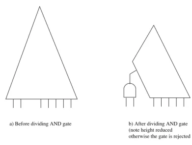
The key idea behind ROBDD division is that we take the ROBDD of a nodenand attempt to divide it with the gates in a library. If such a Boolean division is possible and it is strictly ROBDD depth-reducing, we select it. The test for whether a library gateg, with an associated variableG, divides the ROBDD f ofnis described next. A pictorial view of the
process is shown in Figure 10.
b) After dividing AND gate (note height reduced otherwise the gate is rejected a) Before dividing AND gate
Figure 10. Dividing a Generalized Buffer into a PTL Structure
The Boolean division based test for whether a library gate g divides a ROBDD f can be represented by following logic equations. Here, f is considered to be Completely Specified Function (CSF).
f =G(f +x) + (f)g, whereg≡Gandx⊆g.
Therefore, the upper and lower bounds (U andL) for f are: U=G(f+g) + (f)g
and
L= (f G+f g)
In this case, with quotienth= f+xand remainderr= f g, we can represent f as f =Gh+r
Algorithm 3 describes thetest division procedure without CODCs. This algorithm represents the test performed during division of ROBDD f by a gateg(having a variable G). 2.
Algorithm 3Pseudocode for Division of f byg≡G test division(f,g,G){ if f g6=0then L= (f G+f g)(g⊕G) U = (f G+Gg+ f g)(g⊕G) Z=bdd between(L,U) Z∗=bdd smooth(Z,gvars) R=bdd compose(Z∗,G,g)
ifR= f andbdd depth(Z∗)<bdd depth(f)then return(success,Z∗) end if else return fail end if }
thatgandGare not independent variables, but rather are related asG≡g. We next find a small ROBDDZ(using the functionbdd between, which returns the heuristically smallest ROBDD Z such that L⊆Z ⊆L+U). Next, we smooth out1 the variables of g. If the resulting ROBDDZ∗, withgcomposed back intoG, is identical to f, we return Z∗ as the
quotient.
Figure 11 shows the resulting synthesized PTL circuit obtained after performing PTL synthesis with generalized buffering as described in Algorithm 2.
Primary Inputs Primary Output
Figure 11. Partitioned ROBDD with generalized buffering
1Smoothing is also referred to as Existential Quantification. The existential quantification of f with respect to a variablexis expressed as∃xf = fx+fx. Smoothing a set of variables
D. Generalized Buffering with CODCs
The PTL synthesis methodology with generalized buffering described in the last section attempts to divide the ROBDD of a node with the gates in the library. During the division, the method finds an upperU and a lower boundLon the resulting ROBDD and then select a heuristically minimum ROBDD betweenLandU by using thebdd between procedure. The range of this choice can extended by using CODCs, allowing the final ROBDD size to be be further reduced. In other words, the CODCs can be used to further simplify the logic of a PTL structure. The CODCs can be computed in two manners: one using f ull simpli f y to compute the complete CODCs, and another using approximate CODCs (ACODCs). The ACODCs are computed in a similar manner as mentioned in [27].
When we want to use CODCs (or alternatively ACODCs) during the division process, we first build the ROBDDs of the nodes ofηtopologically from the inputs to the outputs by fetching the nodes from the arrayA in increasing order of index. When we encounter a new noden whose ROBDD f has a depth greater than 5, then we compute its CODCs by using thecompute dcfunction. After CODC computation we try to divide f with the gates in the library by calling thetest division function. The test division makes use of the CODCs of that node to simplify the logic, and is described in Algorithm 5. If the division is successful and if the depth of ROBDD reduces below 5 then we makena new ROBDD variable. Otherwise, we backtrack (in the same manner as described in the case when CODCs were not used) and make one of the fanins ofn a new variable. The fanin which is made a new variable is the one whose topological level is one less than that of n. Algorithm 4 summaries the synthesis flow for PTL synthesis with generalized buffering and using CODCs.
Algorithm 4Pseudo Code for PTL synthesis using generalized buffers and with CODCs η= optimize network(η)
η∗= decompose network(η, p)
A= dfs and levelize nodes(η∗)
i= 1 whilei≤size(A)do n= array fetch(A,i) f = ntbdd node to bdd(n) ifbdd depth(f)≥5then d =compute dc(η∗,n)
forg≡G∈Gate Librarydo f =test division(f,d,g,G) end for ifbdd depth(f)>5then back-track else bdd create variable(n) continue end if else continue end if end while
1. ROBDD Division with CODCs
In principle, we still attempt to divide the ROBDD ofnwith the gates in a library. However, CODCs are utilized during division to simplify the logic further. If such a Boolean division is possibleandit is strictly height-reducing, we select it. The test for whether a library gate g, with an associated variableG, divides the ROBDD f ofnis described next.
In this case, the ROBDD f ofn is considered to be Incompletely Specified Function (ISF). Letd represents the CODCs computed for the noden. Then the division of f with the logic gatesG≡gin the library can be represented by the following equations:
f =G(f +d+x) + (f+d)g, whereg≡Gandx⊆g Therefore, the upper boundU for f is:
U=G(f+d+g) + (f+d)g
The lower boundLfor f is still the same as when CODCs are not used. L= (f G+f g)
The lower bound L can be found by settingx= andd= in the expression for f above. The test we perform when we try to divide a gateg(having a variableG) into the ROBDD
f of nodenwith CODCdis shown in Algorithm 5.
In Algorithm 5, the functionsLandU are ANDed with(g⊕G)to express the fact that gandGare not independent variables, but rather are related asG≡g. We next find a small ROBDD Z (using the function bdd between(), which returns the heuristically smallest ROBDDZsuch thatL⊆Z⊆L+U), which is a Boolean divisor of f. Next, we smooth out the variables ofg. If the resulting ROBDDZ∗, withgcomposed back intoG, lies between
f and f+d, we returnZ∗as the quotient. If we have a valid division then we map the don’t cared of the noden onto a new set of variablesV so that it can be used during the next iteration. The CODCs are mapped using following equations:
Algorithm 5Pseudocode for Division of f byg≡Gusing CODCs test division(f,d,g,G){ if f g6=0then L= (f G+f g)(g⊕G) U = (f G+dG+Gg+f g+dg)(g⊕G) Z=bdd between(L,U) Z∗=bdd smooth(Z,gvars) R=bdd compose(Z∗,G,g)
if f ⊆R⊆ f +dandbdd depth(Z∗)<bdd depth(f)then Q=d(g⊕G) d=∃VQ return(success,Z∗) end if else return fail end if }
d=∃VQ
whereV is the set of variables which lie in the support ofgbut are not present in the support ofZ∗. The re-mapped don’t cares ofn are used for further Boolean division, to
explore additional generalized buffering opportunities for the noden.
E. Conclusion
This chapter describes the PTL logic synthesis using generalized buffering for both cases i.e. with and without CODCs. The methods described in this chapter was implemented and the experimental results are provided in the next chapter.
CHAPTER V
EXPERIMENTAL RESULTS A. Implementation Details
The new PTL synthesis algorithms with generalized buffering were implemented in SIS [24]. The code consisted of reading a circuit (which was decomposed before-hand into 2-input gates and inverters), and then building ROBDDs of its nodes in a topological manner from the inputs to the outputs. When the depth of ROBDD of any node grew beyond 5, division was invoked, as described in last chapter. For PTL synthesis with CODCs, CODCs were computed and used during division. The CODCs computation were done in two manners: one using f ull simpli f y[24] (which will provide complete CODCs) and another using, ap-proximate CODCs (ACODCs) were computed as mentioned in [27]. Results are presented and compared for both styles of CODCs.
The resulting library gates that were utilized for division, and the new ROBDD after division were stored within each node’s data structure. Since the ROBDDs in question were small (with a maximum height of 8), division was performed exhaustively. If the resulting depth after division was greater than 5, then a back-track step was invoked making one of the node’s fanins a new variable. After this we check the nodes which are in the fanout of the fanin node corresponding to the newly created variable. If any of these fanout nodes was already processed, then their ROBDDs were re-computed, and division was re-done. After attempting division (regardless of whether the division succeeds or fails), the depth of the final ROBDD is guaranteed to be less than or equal to 5, allowing for an elegant exit strategy in case division fails.
The next section provides the information about the library used in the PTL synthesis implementation and the process technology used. Subsequent sections, report the delay
and area results for various circuits which were synthesized using the new PTL approach. These sections also compare these results with the corresponding results for a traditional buffer-based PTL synthesis methodology.
A set of benchmark circuits were synthesized using the new PTL synthesis algorithm with generalized buffering. Experiments show a clear advantage of new PTL synthesis algorithms over traditional PTL synthesis. The traditional method used for comparison was similar to that reported in [3].
B. Gate Library
The gate library used in this implementation consisted of the gates AND2, AND3, AND4, OR2, OR3 and OR4. Since any divided gate becomes a new variable, it is required in both its polarities. Therefore, by DeMorgan’s law, we only have non-inverting gates in our library.
The MUX and all gates in the library were characterized for delay in SPICE [28], using a 100nm BPTM [29] process technology. Table B shows the delay and active area of MUX and all gates in the library.
C. Delay
The delay of a synthesized PTL circuit was extracted by finding the longest delay path from any output to any input. Table C compares the delay of the traditionally buffered partitioned ROBDD based implementation, with the generalized buffering methodology (both cases: with and without CODCs). In this table, column 1 lists the example under consideration. Column 2 reports the circuit delay, for the traditional method. Column 3 reports delay for new PTL synthesis algorithm with generalized buffering without CODCs (as a fraction of the delay of the traditional method). Column 4 and 5 report delay number for PTL synthesis
Table I. Delay and active area of gate library Gate Delay(ps) Area(µ2)
MUX 18 0.08 INV 10.26 0.08 Buffer 20.5 0.16 AND2 30.20 0.28 AND3 37.76 0.44 AND4 47.39 0.64 OR2 38.70 0.36 OR3 46.08 0.68 OR4 68.28 1.12
using ACODCs and CODCs respectively (again as a fraction of the delay of the traditional method). Some entries in the table marked as “-”. This indicates that f ull simpli f ywas not able to compute the CODCs for that circuit.
We observe that new PTL synthesis approach with generalized buffering results in a speed-up of about 24% on average, compared to the traditional method (when CODCs were not used). When ACODCs were utilized for generalized buffering speed-up over the traditional method improves to about 29%. We also observe that it is better to use ACODCs than CODCs because of the following reasons:
• f ull simpli f yis not able to compute CODCs for many large circuits whereas ACODCs can be computed robustly for arbitrary sized circuits [27].
• Second, using CODCs instead of ACODCs does not appreciably improve the delay of the PTL circuits. On average the additional improvement is less than 1% (calculated
Table II. Delay Comparison of Generalized and Traditional Buffered PTL
Traditional Buffering Generalized Buffering
Without CODC’s With ACODCs With CODCs
Ckt Delay (ps) Delay Delay Delay
alu2 5125.32 0.53 0.55 0.54 alu4 18849.06 0.45 0.43 -apex6 1519.02 0.73 0.75 0.75 C432 3505.68 0.86 0.79 0.76 C499 1033.20 1.01 1.01 1.01 C880 2264.40 0.70 0.53 0.54 C1908 4017.96 0.74 0.67 0.68 C3540 21056.04 0.71 0.53 -C5315 4949.28 1.04 1.03 1.04 x3 1045.98 0.82 0.82 0.82 i8 1732.32 0.69 0.62 0.6 x1 860.94 0.67 0.67 0.67 pair 2197.44 0.75 0.70 0.70 rot 1870.74 0.82 0.80 0.80 C6288 36024.12 0.94 0.86 -des 2547.54 0.89 0.79 -too large 3130.56 0.52 0.54 0.54 AVERAGE 0.756 0.710
-over the examples for which the CODC method completed).
• The time taken by f ull simpli f y to compute CODCs is much larger than the time required to compute ACODCs. The run time for each PTL circuit synthesis approach is mentioned in Table E.
D. Area
The area calculation was performed by determining the active area of the MUXes and all the library cells. The area numbers for various gates are mentioned in Table B. The number of MUXes is simply the sum of the sizes of each of the partitioned ROBDDs in the design.
Table D compares the active area of the traditionally buffered partitioned ROBDD based implementation, with that of the generalized buffering methodology (with and without CODCs). In this table, Column 1 lists the example under consideration. Column 2 reports the circuit active area for the traditional method. Columns 3, 4 and 5 report the area for the new PTL synthesis algorithm with generalized buffering without CODCs, with ACODCs and with CODCs respectively. The area in Columns 3, 4 and 5 are expressed as a fraction of the area of the traditional method.
The generalized buffers occupy a greater area than the traditional buffers. Due to this the area improvement of the new PTL synthesis approach is not as high i.e. 3% on average when CODCs were not used and 5% when an ACODCs were utilized. On average (computed over the examples for which CODCs could be computed), the CODCs based method exhibits a 1% area overhead over ACODC based method. Again we observe that using CODCs does not result in area reduction over the case where ACODCs are used. This is an additional reason to use ACODCs rather than
Table III. Area Comparison of Generalized and Traditional Buffered PTL
Traditional Buffering Generalized Buffering
Without CODC’s With ACODCs With CODCs
Ckt Area (µ2) Area Area Area
alu2 164.32 0.87 0.86 0.83 alu4 963.68 1.12 1.12 -apex6 305.52 0.95 0.93 0.93 C432 87.12 1.02 0.93 1.10 C499 106.24 0.92 0.92 0.92 C880 136.16 0.80 0.79 0.79 C1908 152.24 0.97 0.93 0.93 C3540 532.88 1.01 0.98 -C5315 540.16 1.12 1.11 1.12 x3 315.76 0.96 0.96 0.96 i8 520.48 0.75 0.72 0.70 x1 120.88 0.96 0.95 0.95 pair 640.32 1.08 1.07 1.06 rot 229.20 0.96 0.96 0.96 C6288 1220.48 1.10 1.06 -des 1808.88 0.94 0.91 -too large 125.68 0.98 0.97 0.97 AVERAGE 0.970 0.950