Electromagnetic Band Gap Structures in MSA
Saleha A. Shaikh
PG student Department of EXTC DJ Sanghvi College ofEngineering
Vile Parle (W) Mumbai, India
Ami A. Desai
PG student, Department of EXTC DJ Sanghvi College ofEngineering
Vile Parle (W) Mumbai, India
Amit A. Deshmukh
Professor and Head, Department of EXTC DJ Sanghvi College ofEngineering Vile Parle (W) Mumbai, India
ABSTRACT
The electromagnetic band gap structures are widely used to suppress pronounced surface waves in antennas with thicker substrate and higher dielectric constant. This paper reviews various application of Electromagnetic band gap structure in microstrip antenna, a band gap characterization of an electromagnetic bandgap structure along with the explanation of various reported configurations of compact electromagnetic band gap structures. Chebyshev tapered electromagnetic band gap distribution is adopted to minimize ripples in the passband caused by the periodicity of planar electromagnetic band gap structure. They are used with ceramic substrate to increase the radiation efficiency of the antenna and are placed along the inset feed line to improve antenna performance, however to reduce mutual coupling it is placed between antenna arrays. A dual band circularly symmetric structure for the enhancement of radiation properties of microstrip antenna is also studied.
Keywords
Electromagnetic bandgap structure, bandgap characterization of Electromagnetic bandgap structure, compact Electromagnetic bandgap structure.
1.
INTRODUCTION
In recent years the applications of microstrip antennas (MSA) on high dielectric constant substrates has received more attention due to their compact size and conformability with the monolithic microwave integrated circuit (MMIC). However, the utilization of a high dielectric constant substrate has some drawbacks like narrower bandwidth and pronounced surface waves. The bandwidth can be improved using a thick and high permittivity substrate, but this excites surface wave propagation. The generation of surface waves degrades the antenna performance. Furthermore, it increases the mutual coupling of the antenna array. To reduce the mutual coupling and the effects of surface waves, the electromagnetic band gap (EBG) structure is inserted between antenna elements [1]. EBG structures are defined as artificial periodic (or sometimes non-periodic) objects that prevent/assist the propagation of electromagnetic waves in a specified band of frequency for all incident angles and all polarization states [1]. Due to their unique band gap features, EBG structures can be regarded as a special type of metamaterials (MTM). Meta (meaning “beyond”), has been used to describe composite materials with unique features not readily available in nature. EBG structures are usually realized by periodic arrangement of dielectric materials and metallic conductors. Its band-gap features are revealed in two ways: the suppression of surface-wave propagation, and the in-phase reflection coefficient [2].
The in-phase reflection feature leads to low profile antenna designs. The feature of surface-wave suppression helps to improve antenna’s performance such as increasing the antenna gain and reducing back radiation. The bandgap characteristics depend on the material structure such as dimensions, periodicity, and permittivity [3]. They are also used in antenna arrays for reduction in mutual coupling. When the EBG parameters are properly designed, the pronounced surface waves are suppressed, resulting in a low mutual coupling. The measured results demonstrate the utility of the EBG structure, and this approach is potentially useful for a variety of array applications [4-8]. Wide stopband and compact size are realized with defected ground structure (DGS). Furthermore, spurline and open stubs are utilized to get higher suppression level of wave propagation in the stopband. Flat passband is achieved by adopting the tapering technology in the EBG configuration to eliminate ripples [9]. This paper summarizes the aforementioned points about EBG.
2.
BAND GAP CHARACTERIZATION
OF EBG STRUCTURE
The mushroom-like EBG structure is shown in Fig.1. It consists of a ground plane, a dielectric substrate, metallic patches, and connecting vias [2]. A distinct stopband for surface-wave propagation is exhibited by this structure. An LC filter array is used for mechanism of the structure. The inductor L results from the current flowing through the vias, and the capacitor C due to the gap effect between the adjacent patches. For an EBG structure with patch width W, gap width g, substrate thickness h and dielectric constant ɛr , the values
of L and C are determined by the following formula [2] :
L = µ0 h
C =
𝑊Ɛ𝑜 (1+Ɛ𝑟)𝜋
cosh
−1
(
2𝑊+𝑔𝑔
)
Where µ0 is the permeability of free space and ɛ0 is the
permittivity of free space,
Frequency band gap can be given as,
ω=
1𝐿𝐶
BW =
∆𝜔𝜔
=
1 ɳ𝐿 𝐶
Where, ɳ is the free space impedance.
(a)
[image:2.595.61.274.72.266.2](b)
Fig. 1. FDTD Simulation model of EBG (a) top view (b) side view [2]
[image:2.595.330.529.136.367.2]In order to obtain a wide range of frequency responses the infinitesimal dipole source with a Gaussian pulse waveform surrounded by the mushroom-like EBG structure is used [2]. Since the E field in MSA application is vertical to ground plane, the dipole is chosen to be vertically polarized. From Fig. 2 It is observed that, when rows of EBG patches are less, the band-gap effect is not significant.
Fig.2. value of IEI2 at the reference plane [2]
However increase in number of rows results in a clear bandgap formation. The average E field inside the band gap is much lower in EBG structures than in non-EBG case. The
basic idea is to calculate and compare the E field at the reference plane. Since the EBG structure can suppress the surface waves in a certain band gap, the E field outside the EBG structure should be weaker than that of the conventional case. To quantify the surface-wave suppression effect, an average E 2 is calculated according to the following equation [2]:
|E|
2=
1𝑠
|E|
2
ds
𝑠Since the above observation shows that the EBG structure has ability to suppress surface waves, four columns of EBG patches are inserted between the antennas to reduce the mutual coupling, as shown in Fig. 3(a).The mutual coupling results are shown in Fig. 3(b).Without the EBG structure, the antennas show a strong mutual coupling of 16.15 dB. If the EBG structures are employed, the mutual coupling level changes. When the 2mm EBG is used, its band gap is higher
than the resonant frequency 5.8 GHz. Therefore, the mutual coupling is not reduced and a strong coupling of 15.85 dB is present. For the 3mm EBG case, the resonant frequency 5.8 GHz falls inside the EBG band gap so that the surface waves are suppressed.
(a)
[image:2.595.63.251.374.525.2](b)
Fig. 3 simulated model: (a) MSA separated by mushroom EBG structure and (b) mutual coupling plot [2]
3.
NOVEL COMPACT EBG
STRUCTURES
3.1
Fork like EBG Structure
The schematic of the proposed fork-like EBG structure is shown in Fig. 4 (a). Each element of this EBG lattice consists of a square metal patch with a slot etched on it and a stretched strip, as shown in Fig. 4 (b) [3]. A metal plated via is used to connect the patch and the ground plane. Additional capacitance is formed between the neighboring edges of the slot and the stretched strip from an adjacent patch. More capacitance can be introduced by increasing the depth of the stretched strip embedded in the slot. Thus, the EBG structure works at a lower frequency, which usually needs a larger size of conventional EBG structures. The range and depth of the stopband of the fork-like EBG exceed those of the conventional mushroom-like EBG.
(a) (b)
[image:2.595.323.537.587.723.2]From Fig. 5 it can be seen that, a distinctive stopband in the horizontal direction, is observed with the central frequency of 4.8 GHz. The frequency range with S21 below 20 dB extends
from 4.63 to 4.98 GHz. In the vertical direction, the edge where the band-gap starts is 60 MHz lower. However, ripples are found in the stopband. This is mainly because of the multipath reflection effect caused by the digitized fingers in the vertical direction.
(a)
(b)
Fig.5. Measured and simulated result for S21 of 5X5: (a) fork-like EBG (b) Mushroom EBG
3.2
Reconfigurable Multiband EBG Design
It was required to design EBG structures of different sizes according to their respective desired frequency band-gaps. When the operating frequency is changed, the EBG dimensions have to be redesigned. However, this limits the application of EBG structures in many cases. The fork-like EBG configuration provides a possibility to construct a reconfigurable EBG structure due to its additional degree of freedom to control the band-gap characteristics [3]. The schematic of the proposed reconfigurable multiband EBG structure is shown in Fig.6. The stretched strip of the fork-like EBG lattice is divided into several segments. MEMS switches are inserted between the segments. The reconfiguration is carried out by switching on or off appropriate stretched strip lengths and the tuning of band-gap position is realized.Fig.6. Configuration of reconfigurable multiband EBG [3]
(a)
(b)
Fig.7.Measured and simulated S21 of the reconfigurable EBG patch array (a) all MEMS switches off and (b) upper
MEMS switches on [3]
As shown in Fig.7, when all the switches are off, the length of the stretched strip is in the shortest situation. The band-gap extends from 5.34 to 6.19 GHz with a central frequency of 5.77 GHz. When the upper switch of each EBG lattice is on, the length of the strips are stretched and the band-gap extends from 4.98 to 5.59 GHz with a central frequency of 5.28 GHz. When all the switches are on, the EBG will work on an even lower frequency.
3.3
Slot–Strip EBG Design Method
The slots and stretched strips used in the design of fork-like EBG structure can be synthesized as a compact EBG design method, which is called the slot-strip EBG design [3]. By applying slots and stretched strips, additional gaps between neighboring EBG patches are introduced as shown in Fig. 8. These gaps significantly enlarge capacitance of the equivalent LC network. A distinctive improvement of EBG size reduction can be observed. The slot-strip EBG design method can be applied to form numerous compact EBG structure configurations.
Fig.9. Simulated S21 of the F-like EBG and normal mushroom-like EBG lattices with the same period [3]
The band-gap feature of the F-like EBG structure is shown in Fig. 9. , and it is compared to a normal EBG structure without slots and strips. In the latter case, the stopband extends from 5.42 to 6.04 GHz. When the slots and stretched strips are incorporated, the frequency band-gap position decreases to3.31–3.66 GHz. Another interesting observation of the F-like EBG structure is that a second frequency band-gap is noted without tuning the stretched strip length. In the case of a normal EBG structure, only one band-gap can be observed below 10 GHz. While using the F-like EBG structure, besides the basic frequency band, the frequency band of the higher mode is also reduced. Thus, a second band-gap appears around 6.7 GHz. In the slot-strip EBG design formations, the band-gap position can be tuned as a common characteristic.
3.4
Tapered EBG with Defected ground
structure for wide stopband
[image:4.595.336.520.322.464.2]A compact tapered EBG structure with defected ground structure (DGS) is proposed to get wide stopband and compact size. Furthermore, spur line and open stubs are utilized to get higher suppression level of wave propagation in the stopband [4]. Flat passband is achieved by adopting the tapering technology in the EBG configuration to eliminateripples.Fig.10 shows the schematic of the one-dimensional EBG structure.
Fig.10. One dimensional EBG structure [4]
The planar EBG structure consists of an array of uniform square patterns etched on the microstrip line. In Fig.10.d1 is
the distance between two adjacent EBG cells, represents the side length of square pattern. According to the photonic crystal theory, the planar EBG structure exhibits a band-gap characteristic while the following Bragg reflection condition is satisfied [4].
ᵦ.d1 = π
ᵦ
=
2𝜋𝜆𝑔
, λg
=
𝑐𝑓0. Ɛ𝑒𝑓𝑓 ……… (1)
Where
ᵦ
is the guided wavenumber of the substrate, λg is theguided wavelength, f0represents the central frequency of the
stopband, c is the speed of light in free space, and Ɛeff is the
effective permittivity that is estimated as,
Ɛ
eff=
(Ɛ𝑟+1)2
+
(Ɛ𝑟−1)
2 1+12/𝑤 ……….. (2) Where Ɛr and h are the relative dielectric constant and the
thickness of the substrate, respectively, and w is the width of the microstripline.
Substituting (2) into (1) yields
d
1=
𝜆𝑔2
=
1 2𝑐 𝑓0 . Ɛ𝑒𝑓𝑓
The filling factor a/d1 plays an important role in the attenuation performance. Owing to d1 is determined as long as the central frequency is selected. Bandwidth and suppression level of the stopband are mainly influenced by a. As shown in Fig.11, the transmission responses of the stopband can be improved significantly as an increases. With increase in a, the capacitance of the square pattern will become larger. This will result in the decrease of central frequency and increase of bandwidth within the stopband. However, the ripple in the passband increases simultaneously with the larger filling factor.
Fig.11. Magnitude of S21 for different values of a [4]
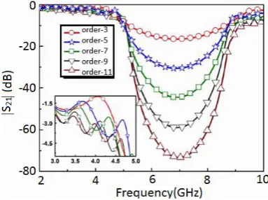
Fig.12. Shows the transmission responses of the planar EBG structures for different orders (number of etched square patterns).The attenuation level and selectivity of the transmission responses become better with increasing order of EBG patterns, whereas the dimension of structure will be larger accordingly. Moreover, as can be seen from Fig.12 the ripples in the passband near the cutoff frequencies are large, which is caused by the periodicity of EBG structure.
[image:4.595.61.276.519.586.2] [image:4.595.332.524.577.720.2]So a large number of cells of EBG structure are still required to improve the stopband performance. Therefore, an effective way to modify the propagation behavior without increasing the structure size must be taken into consideration. Tapering technology is an available method for eliminating the high ripple level in the passband
Fig. 13. Magnitude of S21 for different tapered EBG
structure [4]
[image:5.595.322.532.284.447.2]As shown in Fig. 13, the uniform EBG structure exhibits wide and steep suppression in the stopband, but a high ripple level is obtained in the passband. The performance of EBG structure with different tapering windows are also listed in the Table 1.[4] Significant improvement in the ripple level is achieved by the tapered EBG structure, while the attenuation characteristic in the stopband is sacrificed.
Table 1.Performances of EBG structures with different
tapering windows [4]
Kaiser Chebyshev Gaussian
Ripple(dB) -2.49 -2.14 -3.14
BW(GHz) 4.3 4.77 4.91
Attenuation(dB) -42.54 -47.3 -52.4
For good tradeoff, they have adopted the Chebyshev. DGS, an etched defect in the ground plane that disturbs the shield current distribution, performs a band-gap behavior in some frequency band with only one or more unit patterns Fig. 14. Shows the etched circular shape of the planar EBG structure, which is located on the backside metallic layer. In order to achieve minimization, only two circular DGS patterns are etched underneath the adjacent EBG square patches, respectively. The distance d2 between two circular patterns is equal to the period of EBG structure d1 with the same resonant frequency according to the Bragg reflection condition.
Fig. 14. Planar EBG with DGS [4]
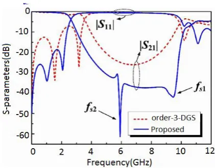
From Fig. 14, the DGS sections are placed under the modified microstrip conductor line and provide the parallel capacitance with effective line inductance. As the etched area of the circular patterns increases, the effective series inductance become larger, which give rise to a lower resonant frequency. Moreover, the radiation loss of the ground plane will be larger, corresponding to the increase of r, which results in a high rejection level of the stopband. The simulated parameters of a traditional fifth-order planar EBG and a third-order planar EBG with DGS are shown In Fig. 15. The wide stopband and low insertion loss are achieved with two DGS circular patterns. However, the attenuation level of the stopband is not so good with the DGS structure. In order to achieve better performance of the stopband without increasing the number of EBG patterns, spurline and open stubs are introduced in the proposed design. From Fig.16, spurline with inherently compact characteristic can be located between two adjacent square patterns.
Fig.15. Simulated S-parameters of the traditional fifth-order EBG structure and third-fifth-order planar EBG
[image:5.595.58.275.424.483.2]structure with DGS [4]
Fig.16. proposed structure with spur line and open stubs [4]
[image:5.595.74.262.631.705.2]Fig.17. Simulated S parameters for EBG structure with DGS and proposed design [4]
Fig. 17. Shows ,the stopband below 20 dB of the third-order planar EBG structure with DGS ranges from 4.93 to 8.59 GHz, while that of the proposed EBG structure ranges from 3.68 to 10.15 GHz. Moreover, the suppression level is deepened from 26 to 42 dB.
4.
VARIOUS APPLICATIONS OF EBG
STRUCTURES
4.1
EBG Structure with Dumbbell-like
Unit Cell
[image:6.595.62.273.69.234.2]A simple and practical method is proposed to reduce the mutual coupling between array elements is as shown in Fig. 18 [5]. An EBG structure with dumbbell-like unit cells (DEBG) is designed to reduce the surface waves around 5.6 GHz. The details of this structure are given in Fig. 19. The square patches of a unit cell have their edges of 2.5 mm long (Lp). The thin line connecting two patches has its width of 0.4 mm (Ws) and a length of 3.6 mm (Ls). The slot between a patch and a line is 0.2 mm wide (Ds).
Fig.18. Configuration of the two antenna arrays (a) without EBG (b) with EBG, upper two – side view; lower
[image:6.595.334.520.172.456.2]two – top view [5]
Fig.19. Dimensions of DEBG structure [5]
Fig.20 (a) shows the comparison of simulated transmission coefficient S21 between the array elements with and without EBG insertion. It is noted that the dumbbell structure can reduce the magnitude of S21 by about 4 dB at 5.65 GHz. Also, the gain is increased by 1 dB as shown in Fig. 20(b).In larger arrays, mutual coupling between elements is critical to a precise design, which needs complex computation and adjustment. If the mutual coupling is attenuated, simpler design and high performance of arrays can be achieved.
(a)
(b)
Fig.20. Comparison of (a) magnitude of S21, (b) magnitude
of gain [5]
(---) without EBG insertion ( ) with EBG insertion
[image:6.595.63.274.486.751.2] [image:6.595.64.278.488.600.2] [image:6.595.76.260.617.753.2]Fig.21. ceramic antenna on EBG substrate [6]
(a)
(b)
Fig.22. radiation pattern (a) ceramic antenna and (b) proposed structure [6]
4.3
EBG Structure Placed along Feedline
A novel placement of EBG structures on both sides of the inset feedline of the MSA as shown in Fig.23. [7] Electromagnetic wave propagation as surface waves along the ground plane instead of radiation into free space reduces the antenna efficiency and gain. The diffraction of surface waves increases the back lobe radiations, which deteriorate the signal-to-noise ratio in wireless communication systems. For the higher bands of frequencies, harmonics exist at operating frequencies, which radiate and contribute to the losses through the feed network. Harmonics can be reduced by using EBG structures that exhibit band-gap characteristics, to suppress the surface waves at the radiating slot of the MSA.(a) (b)
Fig.23. Placing of EBG structure (a) conventional and (b) proposed design (both the sides of feedline) [7]
Table.2 Values of return loss for different positions of EBG structures from the feedline [6]
Sr.No EBG distance from
feedline, mm
Return loss, dB
Resonant frequency, GHz
1 1 22.04 4.635
2 1.5 28.17 4.735
3 2 18.56 4.723
4 2.5 15.41 4.68
Table.2 shows the values of return loss at different position of EBG from feedline. The proposed design was arrived by analyzing the efficiency of antenna when EBG structures are placed at various distances from the feedline. The increase in return loss is because of the suppression of surface waves. When the EBG structures are placed at the feedline, the percentage bandwidth improved by 23% and gain improves by 1 dB. Therefore the placement of EBG structures at the feedline is a critical parameter.
4.4
CS-EBG for Dual Band Application
A dual band circularly symmetric EBG (CS-EBG) is proposed for the enhancement of radiation properties of MSA [8]. The main advantage of the CS-EBG geometries compared to conventional 2-D EBG structures is that a surface wave excited by a source located at its center experiences the same band gap effect in all radial direction. The proposed CS-EBG structure is utilized as antenna substrate to increase the circular microstrip fractal patch antenna performance at both operating frequencies. For the basic structure, a circular MSA has been designed to operate at 1.8 GHz. In the next step, a crescent shape is subtracted from the circular patch. In this way, a dual band circular patch antenna has been obtained as shown in Fig.24. Varying the size of the crescent slot leads to a change in frequency scale factor of this antenna and therefore, the second antenna frequency band can be tuned. The patch is fed by a coaxial probe. The probe should be placed at a position that maximum impedance bandwidth is achieved at both frequency bands. To achieve this, the ratio of distance between excitation point and center of each circle to its radius should be the same for both circles.(a) (b)
Fig.24. Circular patch: (a) single band (b) dual band
Fig.25. CS-EBG structure (a), (b) at 1.8 GHz. (c), (d) at 2.4 GHz. (e) combined dual band. [8]
In order to reduce the surface wave impact, the patch is surrounded by EBG cells. The dual band circular antenna and the tuned CS-EBG cells are integrated in order to achieve the desired objectives. Due to the mutual interaction between the adjacent patches on the CS-EBG operation a modification is required. Therefore the separation between patch and EBG cells is tuned to attain minimum back radiation. The complete integrated antenna is shown in Fig.26 Compared to the reference patch antenna without EBG, the CS-EBG structure has significance that it improves the impedance matching of the antenna.Fig.27, shows the radiation patterns and gain at 1.8 GHz and2.4 GHz have little difference which is one of the inherent characteristics of fractal antennas.
Fig.26. Patch antenna integrated with CS-EBG [7]
(a)
(b)
Fig.27. E plane radiation pattern at (a) 1.8 GHz (b) 2.4 GHZ [7]
4.5
Mushroom-like EBG to reduce RCS
EBG structure is further used to reduce the radar cross section (RCS) of the patch array antenna. The proposition of this method is based on the high impedance characteristic of the mushroom-like EBG structure [9]. Fig.28 shows the proposed design of 2X2 patch array antenna partially covered with mushroom-like EBG. The RCS reductions for the x and y polarized incident waves are different as shown in Fig. 29 and Fig.30.The y-polarized case is better than that of the x-polarized casebecause the main polarization of the antenna is designed in the x-direction.Fig.28. 2X2 patch array antenna with EBG [9]
(a)
(b)
Fig.21. Comparison of RCS of the two patch array antennas with y -polarized incident wave impinging from
(a)
[image:9.595.57.276.76.358.2](b)
Fig. 22. Comparison of co polarization bi static RCS of the two patch array antennas with x -polarized incident wave impinging from normal direction (a) E plane and (b) H
plane [9]
5.
CONCLUSION AND SCOPE OF
FUTURE WORK
This paper briefly reviews Electromagnetic band gap structures. It summarizes various benefits of using EBG
structures such as, improvement in radiation efficiency by increasing gain and reducing side lobe radiation, reduced radar cross section, mutual coupling between antenna arrays and suppression of pronounced surface waves. The exact formulation and modal analysis for the MSA with EBG structure is not mentioned in the papers reviewed which will be explored later in further research.
6.
REFERENCES
[1] Yang, F. and Yahya, R.-S. 2008 EBG structures in antenna engineering, Cambridge University Press, New York , USA.
[2] Yang, F. and Yahya, R.-S. 2003 Microstrip antennas integrated with Electronic band-gap (EBG) structures: A low mutual coupling design for array application, IEEE Transactions on Antennas and Propagation, Vol. 51, NO. 10, October (2936-2946).
[3] Yang, L., Fan, M., Chen, F., She, J. and Feng, Z.,2005.A Novel Compact Electromagnetic-Bandgap (EBG) Structure and Its Applications for Microwave Circuits, IEEE Transactions On Microwave Theory And Techniques, Vol. 53, NO. 1, (January 2005)183-190. [4] Zhu, H. and Mao, J. 2012. Miniaturized Tapered EBG
Structure With Wide Stopband and Flat Passband , IEEE Antennas And Wireless Propagation Letters, Vol. 11. [5] Ang, Y. and Zhang, X. 2003. A Novel Method to
Improve the Performance of Microstrip Antenna Arrays Using a Dumbbell EBG Structure, IEEE Antennas and Wireless Propagation Letters, Vol. 2, 170-172.
[6] Gonzalo, R., Ederra, I. and Iriarte, J.-C. 2010. Design and characterisation of a high efficiency ceramic EBG patch antenna , IET Microw. Antennas Propag., Vol. 4, Iss. 8, 1056–1062.
[7] Bhuvanewari, B.,Malathi, K. and Shrivastav, A. K. 2012. Effect of placing mushroom electromagnetic band-gap structures at the inset feedline of microstrip patches, IET Microw. Antennas Propag., Vol. 6, Iss. 13, 1487–1497. [8] Marzieh, S.-R., J., R.-M. and Edalatipour, M.2012.
Radiation Properties Enhancement of a GSM/WLAN Microstrip Antenna Using a Dual Band Circularly Symmetric EBG Substrate, IEEE Transactions On Antennas And Propagation, Vol. 60, No. 11, November 2012, 5491-5494.
![Fig. 3 simulated model: (a) MSA separated by mushroom EBG structure and (b) mutual coupling plot [2]](https://thumb-us.123doks.com/thumbv2/123dok_us/8028968.768176/2.595.63.251.374.525/fig-simulated-model-separated-mushroom-structure-mutual-coupling.webp)
![Fig. 13. Magnitude of S21 for different tapered EBG structure [4]](https://thumb-us.123doks.com/thumbv2/123dok_us/8028968.768176/5.595.70.264.140.287/fig-magnitude-s-different-tapered-ebg-structure.webp)
![Fig. 22. Comparison of co polarization bi static RCS of the two patch array antennas with x -polarized incident wave impinging from normal direction (a) E plane and (b) H plane [9]](https://thumb-us.123doks.com/thumbv2/123dok_us/8028968.768176/9.595.57.276.76.358/comparison-polarization-static-antennas-polarized-incident-impinging-direction.webp)
