Design of 4-bit Flash ADC using double tail
comparator in 130nm technology
Hemlata Gururani1, Rachna Arya2 1
P.G student, Dept. of electronics and communication Bipin Tripathi kumaon Institute of technology Dwarahat, Almora, Uttarakhand, INDIA
2
Assistant professor, Dept. of electronics and communication Bipin Tripathi kumaon Institute of technology Dwarahat, Almora, Uttarakhand, INDIA
Abstract: The requirement of ultra low-power, area efficient and high speed analog-to-digital converters is pushing toward the use of dynamic regenerative comparators to enhance speed and power efficiency. In this paper a low power double-tail comparator proposed for 4-bit Flash Analog-to-Digital Converter by adding two transistors. The demanding issue in the design of a low power Flash ADC is the design of comparator and Thermometer code to Binary code converter at low supply voltage with low power dissipation.. The implementation of comparator and encoder is done using dynamic CMOS logic to reduce the power consumption of the Flash ADC.The encoder is MUX based thermometer to binary code converterwhich consumes 44.5365mW power. The proposed double tail comparator is designed at supply voltage of 0.8V and compared with the conventional clocked regenerative comparators having minimum power dissipation of 701.1725pW. Then, using this double tail comparator a Flash ADC having 4 bit resolution is designed which dissipates 10.0204uW power with supply voltage 1.8V. The simulation is done using Mentor Graphics back end tool with Pyxis schematic 10.5 version on LINUX operating system.
Keywords- Very Large Scale Integration(VLSI), Analog to Digital Converter (ADC), Digital to Analog Converter (DAC), Complementary Metal Oxide Semiconductor(CMOS), Double Tail Comparator (DTC), Multiplexer(MUX).
I. INTRODUCTION
The field of communication has evolved significantly leading to the growth of many low cost integrated circuits of which Analog to digital converters (ADC) are important. The requirement of today’s world where demand for portable battery operated devices is increasing which encourage design of a low power, high speed and low cost ADC. Among several analog-to-digital converters, Flash ADCs are mainly used in high speed applications and are known for its high power consumption [1] [7]. Analog circuits are commonly used in more power constrained situations. The power consumed by the digital CMOS logic is directly proportional to the square inverse of the scaling factor (k).
Digital Power ∞ k-2 (1) On the other hand, analog power consumed by CMOS flash ADC scales with the inverse of scaling factor when bandwidth
is held constant.
Analog Power ∞ k-1 (2)
As the CMOS technology enhances, the power consumed by
digital circuits scales faster than the power consumed by analog circuits, making the digital logic more and more attractive to reduce the analog difficulty. This has directed the path to a great deal of research on digital techniques to enhance the performance of simple, low resolution analog circuits in ADCs [2].
Fig.1 Flash ADC architecture
he exponential growth in the usage of battery operated devices like cell phones, tablets, laptops and portable medical instruments has made power consumption one of the most prominent design criterions. There is a need for power efficient designs, consuming a small area because the fabrication cost of the chip is directly proportional to its area. The System on chip has reduced the total power consumption and area requirement of the devices and brought significant performance improvements.
The structure of this paper is organized as follows:
In Section II, the related work together with the contributions is discussed. In Section III the internal proposed blocks of comparator and encoder with their integration to design a Flash ADC is discussed. Section IV evaluates the performance of the proposed Flash ADC through experimental simulation and comparison table. Section V gives the conclusion of the paper.
II. RELATED WORK
The papers related to the topics are studied to know the scope in the field for innovation, research and development. For a Flash ADC commonly used encoders has been ROM / PLA circuits, XOR encoder, fat tree encoder and Wallace tree encoder [1]. In [2], an area efficient low power high Speed 3-bit Flash Type ADC using bit referenced encoder is proposed in 180 nm CMOS technology. The main drawback of flash ADC is that it requires large area and dissipate huge amount of power. To overcome this complexity numbers of comparators are reducing by using multiplexers and are used to generate reference voltages [3]. In [4], a 4-bit flash analog to digital converter for low power SOC application is presented. CMOS inverter has been used as a comparator and by adjusting the ratio of channel width and length, the switching threshold of the CMOS inverter is varied to detect the input analog signal. In [5], the design of 4 bit Flash ADC is presented using Threshold Modified Comparator Circuit(TMCC) and NOR ROM encoder. The TMCC comparator eliminates the resistor ladder network which reduces area and power consumption. In [6], the analysis and design of a low voltage low power double tail comparator is presented. The proposed double tail comparator which is used in this paper for designing the Flash ADC is based on the double tail comparator structure given in paper[6]. Fig.2 shows the schematic diagram of double tail comparator.
The working of the modified double tail comparator is completed in two phases. The two modes are reset mode and evaluation mode. In reset mode CLK=0, both the tail transistors Mtail1 and Mtail2 are off which avoids static power consumption. The transistor M3 and M4 pulls both the fn and fp nodes to VDD which cutoff control transistors Mc1 and Mc2. Intermediate stage transistors MR1 and MR2 reset both latch outputs outn and outp to ground.
Fig.2 Circuit diagram of double tail comparator
control transistors are still off. According to the input voltages fn and fp start to drop with different rates.
Assume VINP > VINN thus, fn drops faster than fp. As long as fn continues falling the corresponding pMOS control transistor Mc1 starts to turn on. Then Mc1 pulls fp node back to the VDD and Mc2 remains off allowing fn to be discharged completely. In this structure when the comparator detects fn discharges faster, pMOS transistor Mc1 turns on which pulls fn node back to VDD. In modified double tail comparator as the time passes, the difference between fn and fp increases in an exponential manner which reduces the latch regeneration time. In this circuit when one of the control transistor (Mc1) turns on, a current from VDD is drawn to the ground via input and tail transistor(Mc1, Mc2 and Mtail1) which results in static power consumption. So, two nMOS switches are used below the input transistors to overcome this issue.
III. PROPOSED FLASH ADC AND ITS INTERNAL BLOCKS
The block of Flash ADC is divided into three Major blocks. These blocks are resistor ladder, set of comparators and encoder.
A. Resistor ladder
Resistor ladder divides the reference voltage Vref into 16 levels. Resistor ladder block is shown in fig.3. In circuit 16 resistors of 1
KΩ are used from device library of Pyxis tool. The output of the resistor ladder is given to comparator block. The reference voltage
Fig.2 Schematic diagram of resistor ladder
250mV, 225mV, 200mV, 175mV, 150mV, 125mV, 100mV, 75mV, 50mV and 25mV.
B. Proposd double tail comparator
In this paper, a novel low power high performance double tail comparator circuit is presented. It is designed by adding extra pMOS and nMOS transistor in series with tail transistors. The proposed design achieves better speed and power performance as compare to the double tail comparator as shown in fig.2.The working of this comparator is same as the working of double tail comparator. The power dissipation parameter decreases to a greater extent as compare to the delay parameter.
The major challenge for designing the proposed double tail comparator is to design a low power comparator which can operate in low supply voltage. The proposed double tail comparator is designed by considering following points:
The main contributors to the comparator delay have been analyzed. Based on this analysis a new double tail comparator designed. The circuit of the double tail comparator is modified for low power and fast operation even in small supply voltage by adding one pMOS transistor with top tail transistor and one nMOS transistor with bottom tail transistor. Both transistors are given clock pulse. Hence the proposed double tail comparator is designed by using clock gating technique.
The adjustment of the ratio of (W/L) of the MOS transistors makes the changes in the rise time and fall time. Hence, the nMOS and pMOS having different (W/L) ratios are used.
For nMOS, W = 1000nm =1um, L = 130nm= 0.13um For pMOS, W = 2000nm =2um, L = 130nm = 0.13um
The schematic diagram of proposed double tail comparator is shown in Fig.3.
Fig.3 Schematic diagram of double tail comparator
Fig.4Transient response of proposed double tail comparator
C. Thermometer code to Binary code Encoder
The output of the comparator is in the form of Thermometer code. Hence, an encoder is needed to convert the thermometer code into the binary code. The working of thermometer to Binary code converter is explained. Thermometer code input T8 is equivalent to the gray code G3. So B3 is directly taken from T8. To get G2, the input T12 is taken as select line of MUX CELL01. T4 is connected to input ‘0’ of CELL01 and input ‘1’ is grounded. For G1, T14 is taken as select line for MUX CELL02 and T6 is connected to the select line of MUX CELL03. When T6 is ‘0’, T2 is equivalent to G1. When T6 is ‘1’, output of CELL02 is selected. Considering CELL02, When select line is ‘0’, then T10 is selected for G1. For T14 equal to ‘1’, G1 is ‘0’ so the input of CELL02 is grounded. For getting G0, first give T13 to input ‘0’ and ground the input ‘1’ of MUX CELL04 by taking T15 as the select line. Output of CELL04 is given to input ‘1’ of MUX CELL05 and T9 to input ‘0’ by taking T11 as select line. The output of CELL05 is given to input ‘1’ of MUX CELL06 and T5 to input ‘0’ by taking T7 as select line. The output of CELL06 is given to input ‘1’ of MUX CELL07 and T1 to input ‘0’ by T3 as select line.G0 is taken from the output of CELL07 Here the grounding concept is used to reduce the hardware, which in turn reduces the overall power consumption.
The boolean expressions for this conversion are given below: G3 = T8
G2 = T4 12
G1 = T2 6+(T10 14)T6
G0 = T1 3+(T5 7+(T9 11+(T13 15)T11)T7)T3
Then, the conversion of the gray code to binary code is completed using the general form by XOR gate. B3=G3
Fig.5 Schematic diagram for simulation of proposed encoder
The complete architecture of the proposed encoder is shown in Fig.5. It consists of 7 2:1 and 3 XOR gate. This proposed architecture has lowest number of transistors among all the 4 bit thermometer to binary code converter architectures reported in the literature. So the total area requirement is less which helps in reducing the power consumption. The total power dissipation of simulated encoder is 44.5365nW. Fig.6 shows the transient analysis results of 4-bit proposed thermometer-to-binary encoder.
Fig.6 Simulation Output waveform for proposed encoder
D. Final implementation of proposed Flash ADC
Fig.7 Schematic diagram of Flash ADC
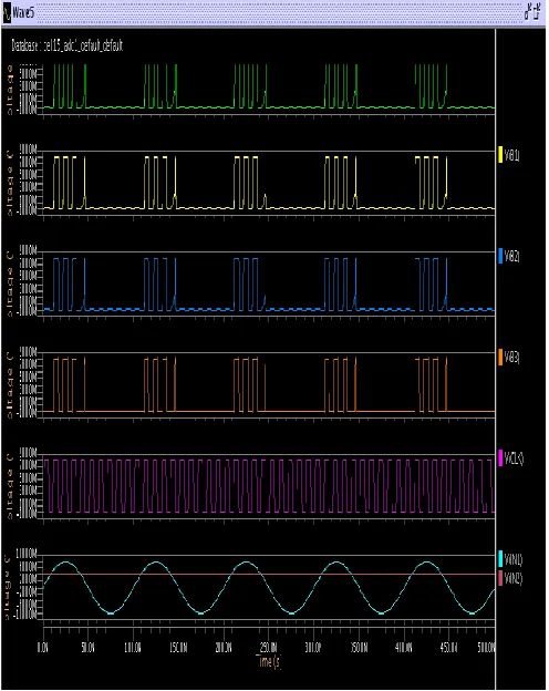
Fig. 8 Transient response of Flash ADC
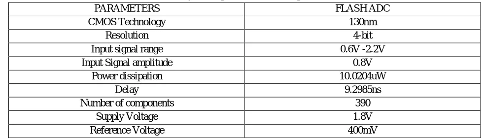
[image:8.612.183.431.360.672.2]Power dissipation 10.0204uW
Delay 9.2985ns
Number of components 390
Supply Voltage 1.8V
Reference Voltage 400mV
[image:9.612.58.549.141.282.2]Table I. shows the summary of the performance of 4 bit Flash ADC.
Table II. Comparison of present work with earlier work for Flash ADC
Specification [11] [12] [13]
Proposed Flash ADC
Technology 180nm 90nm 130nm 130nm Supply
voltage
4V 1.5V 1V 1.8V
Resolution 4 bit 4 bit 3 bit 4 bit Input range 0V-1.8V - - 0.6V-2.2V
Power dissipation 49.94 mW 1.984 mW 142.89 uW 10.0204 uW
The comparison table II shows the comparison of the proposed Flash ADC with the previous Flash ADC designed using same or different technology. It concludes that the proposed Flash ADC shows improvement in terms of power dissipation, resolution and input voltage range in comparison to previous work.
V. CONCLUSION
In this paper, the 4 bit Flash ADC is designed using 130 nm CMOS technology in Mentor Graphics software. Its internal blocks like resistor ladder, double tail comparator and MUX based Thermometer code to Binary code encoder are designed and simulated. The main advantage of proposed architecture is that the static power consumption is very less as shown in comparison table II. The average power consumed by the proposed Flash ADC is 10.0204uW with delay of 9.2985ns with supply voltage of 1.8V.
REFERENCES
[1] Vinayashree Hiremath, Student Member IEEE; Saiyu Ren, Member IEEE, “A Novel Ultra High Speed Reconfigurable Switching Encoder for Flash ADC”, 978-1-4577-1041-4/11/$26.00 ©2011 IEEE
[2] Aditi Kar, Alak Majumder; Abir Jyoti MandaI; Nikhil Mishra, “Design of Ultra Low Power Flash ADC using TMCC & Bit Referenced Encoder in 180nm Technology”, 2015 International Conference on VLSI Systems, Architecture, Technology and Applications (VLSI-SATA), 978-1-4 799-7926-4115/$31.00©20 15 IEEE
[3] Megha R, Pradeepkumar K A, “Implementation of Low Power Flash ADC By Reducing Comparators”, International Conference on Communication and Signal Processing, April 3-5, 2014, India.
[4] Sudakar S. Chauhan1, S. Manabala, S.C.Bose and R. Chandel,” anew approach to design low power cmos flash a/d converter”,International Journal of VLSI design & Communication Systems(VLSICS) Vol.2, June 201
Scale Integration (Vlsi) Systems, Vol. 22, No. 2, February 2014
[7] Sail, E.; Vesterbacka, M.; , A multiplexer based decoder for flash analog to- digital converters, TENCON 2004. 2004 IEEE Region 10 Conference , vol.D, no., pp. 250- 253 Vol. 4, 21-24 Nov. 2004.
[8] S. Sheikhaei, S. Mirabbasi, A. Ivanov, " An encoder for a 5GS/s 4-bit flash ADC in 0.18/spl mu/m CMOS ", Canadian Conference on Electrical and Computer Engineering IEEE, pp 698-701, May 2005
[9] Kaess, F. ; Kanan, R. ; Hochet, B. ; Declercq, M. “New Encoding Scheme For High-speed Flash ADC’s”, IEEE International Symposium on Circuits and Systems, pp. 5- 8 vol.1, 1997.
[10] Gupta, Y. ; Garg, L. ; Khandelwal, S. ; Gupta, S. ; Saini, S., “Design of low power and high speed multiplexer based Thermometer to Gray Encoder”, IEEE International Symposium on Intelligent Signal Processing and Communications Systems (ISPACS), pp. 501- 504, 2013
[11] Channakka Lakkannavar, Shrikanth K. Shirakol, Kalmeshwar N. Hosur “design, implementation and analysis of flash adc architecture with differential amplifier as comparator using custom design approach” International Journal of Electronics Signals and Systems (IJESS) ISSN: 2231- 5969, Vol-1 Iss-3, 2012. [12] Arunkumar P Chavan Rekha G P Narashimaraja, “An Efficient Design of 3bit and 4bit Flash ADC” International Journal of Computer Applications (0975 –
8887) Volume 61– No.11, January 2013