International Journal of Emerging Technology and Advanced Engineering
Website: www.ijetae.com (ISSN 2250-2459,ISO 9001:2008 Certified Journal, Volume 3, Issue 12, December 2013)
577
Design And Implementation of Low-Cost Power Efficient
Embedded Control Systems in Domestic Induction Heating
Appliances
S. Shanthi
1, S. Muthukrishnan, M.TECH(PH.D)
2 1PG Scholar, Sri Eshwar College Of Engineering,Coimbatore, 2Head of The Ece Department, Sri Eshwar College Of Engineering,
Abstract
-
The proposed modulation technique of power converter topology provides high reliability, excellent performance, minimum energy consumption which reduces switching loss. The Power converter features a full-bridge resonant converter operating with a switching frequency ( ) between 15 kHz and 40 kHz in order to improve efficiency and power density make a suitable solution for domestic induction heating appliances. The digital control systems of these appliances require performing accurate and smooth power control while assuring the safety of the power devices. In order to accomplish, it is necessary to provide the target output power and specific current parameters selected by the user. A/D converter subsystem digitizes the output current. ΣΔ ADCs combines oversampling and the shaping of the quantization noise to achieve high accuracy, which makes them a cost effective and power efficient solution.Keywords—Analog To Digital Converter, Digital Control,
Induction Heating, Resonant Power Conversion.
I. INTRODUCTION
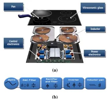
Induction heating appliances are widely used in domestic appliances due to advancement in power electronics and digital control. It is most preferable due to its high performance, efficiency, power control, safety and cleanness [1]. The general architecture consists of the user interface, power converter topology, and digital control system as depicted in Figure (1). The user interface subsystem allows the user to provide the target power delivered to the load. The power converter subsystem, in which the ac mains voltage is rectified and filtered, provides a dc voltage.
(a)
[image:1.612.349.534.258.430.2](b)
Figure 1: Shows the Domestic Induction Heating Application (a) General Architecture (b) Power Conversion Scheme
Then, an inverter, supplies a variable current of 15 to 40 kHz frequency to the induction coil. This alternating current gives a magnetic field alternating in nature, which produces eddy current and magnetic hysteresis heating up the induction pan. Thus the power converter delivers the main target power to the induction load. The inverter is the most essential subsystem of the induction heating appliances. Many different topologies have been proposed for implementing the subsystem are the series resonant half-bridge inverter [2], full-bridge [3], single-switch resonant inverter [4]. Among these choices the full-bridge topology is preferred widely. The choice is based on the balance between cost, operating efficiency and performance.
International Journal of Emerging Technology and Advanced Engineering
Website: www.ijetae.com (ISSN 2250-2459,ISO 9001:2008 Certified Journal, Volume 3, Issue 12, December 2013)
578
[image:2.612.348.533.141.263.2]The target power can be controlled by adjusting using the power delivered to the load in the range of 100 W to 3.3 kW. In the domestic appliances, an accurate and smooth power control is necessary the user needs. Moreover, the heat appliances should operate in a wide operating range. Modulation schemes play a vital role to the above mentioned strategies. To obtain the target output and efficiency, the full-bridge inverter topology through the variable-frequency data cycle control have been proposed [1]. Space Vector Pulse Width Modulation technique is also proposed to reduce the switching loss and harmonics with increased accuracy.The modulation techniques should work under soft switching conditions (i.e.,) zero-voltage switching conditions [6].
Figure 2: Block Diagram of Induction Heating Appliance
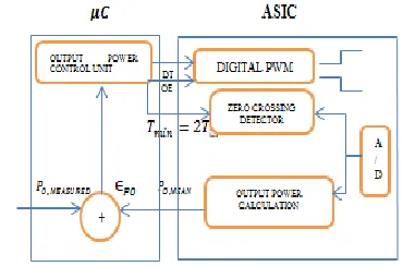
To obtain these operating conditions, it is important to have exact information about the induction load. The induction system can be modelled as the series combination of a RL circuit [10]. These values depend upon the material of the pan, exciting frequency, operating temperature, geometry of the pan. The inverter is assured to be kept inside the Safe Operation Area (SOA) [9], output power and efficiency. The digital control system handles the proper power delivering to the load by adapting the modulation factors such as peak value of the output current( ), root mean square value of output
[image:2.612.61.276.310.431.2]current( ), peak value of output voltage( ). These parameters are measured for each half period of the main cycle. The digital control system can be classified as control block and measurement block [7]. The control block produces the triggering signals of power MOSFET devices considering user defined target output power. The measurement block computes the required current values from the reconstructed output current provided by ∑∆ ADC [1]. Regardless the information, that the entire system will be implemented in an ASIC as shown in Figure (3).
Figure 3: Digital Control architecture based on Microcontroller and an ASIC
The FPGA can be used to evaluate the induction heating system [10]. The output current is put into digital form using sigma-delta ADC. The preference of ADC is due to the advantages of shaping of the quantization noise and oversampling to achieve good accuracy, to become a cost-effective and efficient solution [13]. The INDUCTION HEATING system is a low-cost appliance, this work proposes the entire system as a cost-effective solution. The voltage and current waveforms are put as conditioned output current x (t) by using a sigma-delta ADC [11] into a 1-bit data stream, which is directly processed to obtain
the harmonic impedence at a provided frequency. Then by using digital LPF block reconstructs the output current
by filtering .
The aim of the work is to propose a modulation technique to improve the output power control and efficiency of an inverter applied to domestic induction heating [12]. The inverter topology is a variation of the series full-bridge featuring Power MOSFETs. Power MOSFETS have been applied to IH that allows using an improved modulation scheme [13]. The proposed scheme achieves output power variation, which simplifies the control strategy [12]. Power MOSFETs provide fast switching speed and ruggedized device design [7]. Moreover, it is widely preferred for all applications at power dissipation levels to appropriately 50W. This paper is proposed as follows:
International Journal of Emerging Technology and Advanced Engineering
Website: www.ijetae.com (ISSN 2250-2459,ISO 9001:2008 Certified Journal, Volume 3, Issue 12, December 2013)
579
II. PROPOSED INVERTER TOPOLOGY
The proposed power converter topology is based on the full bridge rectifier which achieves the good balance between cost and performance considering the domestic induction heating appliances. In the proposed method, the IGBT have been replaced by POWER MOSFETS [5]. The power MOSFET provides additional characteristics which allow the increased efficiency and output power control [10]. The Section A includes SVPWM representation [15]. Section B describes the steps needed to realize SVPWM algorithm.
A. SVPWM Representation
In contrast to PWM as triggering signal to the power MOSFET, SVPWM method provides three modulating signals as a single unit called the reference voltage and its component plane is cited in Figure (4). This reference voltage refers 3 variable signals; the switching functions can be modelled as
{
= {
= {
[image:3.612.350.540.284.358.2]
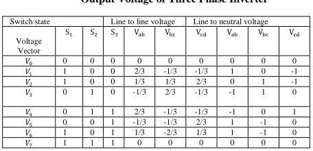
Where are the switching states of the switches in which upper switches are complementary with lower switches as shown in Figure (5).The various combinations of switching states yield upto eight possible in vector ( ) non voltage vectors ( and ). All the combinations and the corresponding output voltage for each state are provided in Table 1.
Table 1
Output Voltage of Three Phase Inverter
[image:3.612.324.538.468.586.2]Figure 4: Voltage Space Vector and its Component Plane
Figure 5: Reference Vector as a Combination of Adjacent Vector
B. SVPWM Algorithm:
The summarization of an algorithm can be done in 2 steps:
STEP1: The first step is to find out and angle (α)
by using the following equations which use abc to park transformation [15].
= - .cos60- .cos60 (1)
=0+ .cos30- .cos30 (2)
[ ] [
√ √ ] (3)
[ ] √ (4)
a= =2П t (5) Where - fundamental frequency.
STEP 2: Computation of time duration. To determine the time duration for the corresponding vectors . To calculate the switching time duration the following equations are applied:
√ | ̅̅̅̅̅| ( (6)
Switch state Line to line voltage Line to neutral voltage Voltage
Vector
[image:3.612.41.269.555.665.2]
International Journal of Emerging Technology and Advanced Engineering
Website: www.ijetae.com (ISSN 2250-2459,ISO 9001:2008 Certified Journal, Volume 3, Issue 12, December 2013)
580
√ | ̅̅̅̅̅̅̅̅̅ |(
) (7)
(8)
Where n=1 through 6 (that is sector 1 to 6) 0 ≤ α ≤ .
Comparison of PWM and SVPWM:
a. SVPWM has better utilization of of 15%Vdc voltage which means more voltage utilization as compared to PWM.
b. SVPWM uses only one reference unit to generate three-phase sine wave.
c. SVPWM gives less total harmonic distortion (THD) and less switching loss.
d. More advanced vector control can be implemented in SVPWM; due to fact that the reference space vector is a two-dimensional quantity.
III. FULL BRIDGE RECTIFIER TOPOLOGY
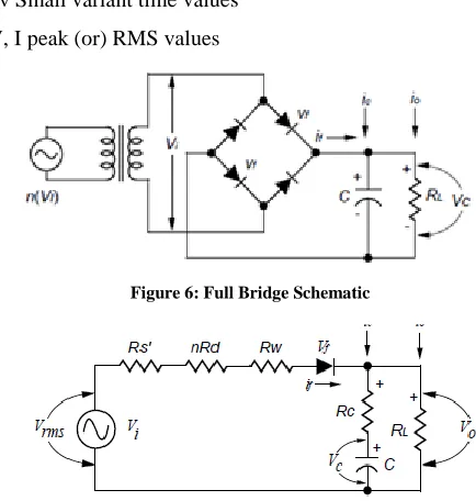
The proposal uses a full bridge rectifier as shown in Figure (6) in which -forward current through the rectifier diodes,
-Output current -Capacitor current
[image:4.612.54.271.457.685.2]i,v Small variant time values V, I peak (or) RMS values
Figure 6: Full Bridge Schematic
Figure 7: Equivalent Circuit for Full Bridge Rectifier with Appropriate Values
The transformers turns ratio, n=
Where -number of turns in the primary windings as shown in Figure (7).
-Number of turns in the secondary windings
-Transformer leakage inductance -Resistance of transformer windings -DC resistance of the secondary winding -DC resistance of the primary winding
(9)
A.Qualitative Analysis Of Voltage And Current:
The input voltage (VI) is a rectified voltage of the form
| | (10)
Where =2Пf, =t, which is the half-cycle period of the AC input voltage.
Figure8: Full Wave Rectified Sine Wave
is the driving voltage and is related to .
(11) At t=0, capacitor will be charged, with a resultant voltage ( ). The rectifier will be forward biased until is
equal to or greater than . This point of time is designated as signifying turn-on and the initiation of rectifier flow ( ) which will increase over time as continues to increase faster than . Thus, the minimum ripple voltage occurs at . As if begins to flow, that is dependent upon the ratio of and the value of C. This current pulse will peak before the incoming voltage does, at time , at a cut-off angle . is the critical point at
International Journal of Emerging Technology and Advanced Engineering
Website: www.ijetae.com (ISSN 2250-2459,ISO 9001:2008 Certified Journal, Volume 3, Issue 12, December 2013)
581
Hence, maximum ripple voltage occurs not at off-condition of rectifier, but at time when =0. Second,
the capacitor will discharge at a rate that can be computed by using exponential decay at time . If the load draws a constant current the capacitor voltage will linearly decay. The discharge will continue through time until overcomes at a time .Moreover, does not perfectly tracks if =0 [15].
IV. SIMULATION RESULTS
A.Schematic Circuit:
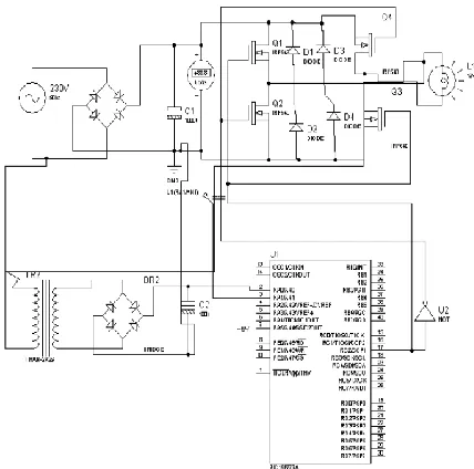
The proposed induction heating appliances obtains 230V AC input voltage from the supply mains which is then rectified by the full-bridge topology and inverted by using power MOSFET triggered by using the proposed SVPWM pulses as depicted in Figure (9). The user provided target output power is fed to the control unit.
Figure 9: Circuit Diagram of the Proposed System Using Proteus Software
The measurement block computes the measured values and digital control unit adjusts the power delivering to the load. The system has been designed 1 kW supply to an induction load.The switching frequency is between 15 kHz to avoid noise. To operate in the appropriate operation mode the resonant frequency should be lower. The power converter is provided from a supply voltage of 230 V, 50 Hz by means of a full-bridge rectifier. In addition to that, some additional capacitors have been added to obtain a better system. The digital control subsystem general architecture is made up of a microcontroller and an ASIC.
The microcontroller monitors the modulation parameters provided by the user through interface unit, whereas the ASIC unit generates the triggering signals for the MOSFETs as obtained in Figure (10). In addition to that, the parameter output current ensures the particular operating mode and achieves the target output power. The proposed inverter specifications are summarized in Table 2.
[image:5.612.330.547.243.480.2]Proposed Inverter Topology:
Table 2
Specifications of Proposed Inverter Topology
Figure 10: (A) Ac Input Voltage ( (B) Triggering Signal for MOSFET S1. (C) Triggering Signal for MOSFET S2. (D) Output
Voltage (
The simulation results of the proposed method are shown in Figure (10). (a) Shows the AC input voltage 230 V with frequency=50 Hz. (b) Triggering Signal for MOSFET with voltage=3.5 V with frequency=50Hz.
(c) Triggering signal for MOSFET voltage=3.5 V frequency=50 Hz. (d) AC output voltage with frequency=50 Hz.
The proposed technique behaves as expected, verifying the results. The plot between switching frequencies versus output power is shown in Figure (11) with the ranges
between 15 kHz to 35 kHz and the corresponding output power varies from 500 W to 1180W.
PARAMETER VALUE
15kHz
40kHz
230
[image:5.612.60.274.347.559.2]International Journal of Emerging Technology and Advanced Engineering
Website: www.ijetae.com (ISSN 2250-2459,ISO 9001:2008 Certified Journal, Volume 3, Issue 12, December 2013)
[image:6.612.66.272.144.280.2]582
Figure 11: Theoretical and Simulation Results for the PowerConverter Output Power Control
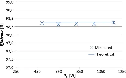
The efficiency plot for the proposed converter is 98.4% for which the output power control varies linearly as shown in Figure (12).
Figure 12: Efficiency Plot for the Proposed Converter Strategy
V. CONCLUSION
Efficiency is the key concern for an induction heating appliance; hence it reduces the energy consumption and also increases the reliability of the output power. In this paper, a new converter based on the full bridge topology has been presented. This converter uses the power MOSFET inorder to allow using a specific modulation technique. This modulation scheme reduces the switching losses and minimizes conduction losses and improves the converter efficiency. Moreover, the output power can be easily controlled by switching frequency, thus avoids the issues in other topologies.
Simulation results confirm that feasibility of the proposed converter and the modulation strategy. As a result, the improved frequency and linear output power control makes this topology very well suited for the domestic induction heating appliance.
REFERENCES
[1] Acero.J, et al., Mar./Apr. 2010 "Domestic induction appliances," IEEE Ind. Appl. Mag.,vol. 16, no. 2, pp. 39-47.
[2] Sarnago.H, Lucía.O, Mediano.A, and Burdío 2013 "Class-D/DE dual mode- operation resonant converter for improved-efficiency domestic induction heating system," IEEE Trans. Power Electron., vol. 28, no. 3, pp. 1274-1285.
[3] Chudjuarjeen.S, Sangswang.A, and Koompai.C June 2011 "An improved LLC resonant inverter for induction-heating applications with asymmetrical control," IEEE Trans. Ind. Electron., vol. 58, no. 7, pp. 2915-2925.
[4] Lucia.O, Burdio J.M, Barraging L. A, Carretero C., and Acero Nov. 2011, "Series resonant multiinverter with Discontinuous-mode control for improved light-load operation," IEEE Trans. Ind. Electron., vol. 58, no. 11, pp. 5163-5171.
[5] Ha Pham N, Fujita H., Ozaki K., and Uchida N. Nov. 2011, "Phase angle control of high-frequency resonant currents in a multiple inverter system for zone control induction heating," IEEE Trans. Power Electron., vol. 26, no. 11, pp. 3357-3366.
[6] Jiménez O., Lucia O, Barragan L. A., Navarro D, Artigas J. I., and Urriza I. 2013. "FPGA-based test-bench for resonant inverter load”. [7] Jiménez O., Lucia O., Urriza I., Barragán L. A., Mattavelli P., and
Boroyevich D., 2013 "FPGA-based gain-scheduled controller for resonant converters applied to induction cooktops," IEEE Transactions on Power Electronics, no..
[8] Egalon J., Caux S., Maussion P., Souley M., and Pateau O. , September/October 2012, "Multiphase system for metal disc induction heating: Modeling and RMS current control," IEEE Transactions on Industry Applications, vol. 48, no. 5, pp. 1692-1699. [9] Lucia O., Burdio J. M., Millan I., Acero J., and Puyal D., , Aug. 2009"Load-adaptive control algorithm of half-bridge series resonant inverter for domestic induction heating," IEEE Trans. Ind. Electron., vol. 56, no. 8, pp. 3106- 3116.
[10] Hwang S. H., Liu X., Kim J. M., and Li H. , Feb. 2013, "Distributed digital control of modular-based solid-state transformer using DSP+FPGA," IEEE Trans. Ind. Electron., vol. 60, no. 2, pp. 670-680.
[11] Acero J., Navarro D.,. Barragan L. A, Garde I., Artigas J. I., and Burdio J. M, Aug. 2007., "FPGA-based power measuring for induction heating appliances using sigma-delta A/D conversion," IEEE Trans. Ind. Electron., vol. 54, no. 4, pp. 1843-1852.
[12] O. Lucia O., Burdio J. M.,. Barragan L. A, Acero J., and I. Millan, , Nov. 2010 "Series- resonant multiinverter for multiple induction heaters," IEEE Trans. Power Electron., vol. 25, no. 11, pp. 2860-2868.
[13] Sung G. M., Yu C. P.,. Hung T. W, and Hsieh H. Y. Feb. 2012, "Mixed-mode chip implementation of digital space SVPWM with simplified-CPU and 12-bit 2.56 Ms/s switched-current delta-sigma ADC in motor drive," IEEE Trans. Power Electron., vol. 27, no. pp. 916-930,.
[14] Ortmanns M. and Gerfers F. Springer, 2006, Continuous-time sigma-delta A/D conversion: Fundamentals, performance limits and robust implementations.
[image:6.612.63.274.358.488.2]