ABSTRACT
In this paper a method to build a faster array multiplier based on Radix 4 Modified Booth Encoder - which is broadly used for the signed multiplication applications- with less area and power is presented. This is achieved by optimizing the overall interconnection delay in the partial product array and by scheming the most efficient Full Adder and Booth Encoder in Complementary Pass Transistor Logic approach. The proposed array multiplier’s performance in terms of delay, power and area is compared with conventional as well as Baugh-Wooley Multiplier. In order to optimize the power and area of the multiplier, a CPL Based MBE with standard partial product array is proposed and designed in full custom style. The use of efficient 10 Transistor based Full adders based on CPL logic ensures that the entire design is in CPL logic, which provides a regular outline with less interconnection intricacy.
Key Words
Modified Booth Encoder, Array Multiplier, Radix-4 Multiplier, Low Power multiplier, Fast Multiplication
1.
INTRODUCTION
Digital signal processing (DSP) and multimedia applications require flexible processing ability, low power consumption and high performance. Multipliers are widely used in DSP and multimedia applications [15].Incessant advances of microelectronic technologies make enhanced use of energy, encode data more effectively, transmit information more reliable, etc. Particularly, many of these technologies address low-power consumption to meet the requirements of various portable applications [14].
There are diverse entities that one would like to optimize when designing a VLSI circuit. These entities can often not be optimized simultaneously, because one entity can be superior only at the expense of one or more others. The design of a proficient integrated circuit in terms of power, area, and speed simultaneously, has become a very demanding problem. With the progression in Digital multimedia applications in Portable devices, delay considerations become the most vital criteria for the VLSI Design. Hardware design which requires high performance is the most imperative consideration in the Microprocessor and DSP design. However area and speed are two contradictory constraints. Hence improving speed always results in larger areas of the IC. In this design the key idea is to optimize the delay while not distressing the power dissipation of the overall circuit.
Low power design is indispensable to condense the casing and cooling expenses as well as prolong the life span of integrated
circuits (ICs). The subsequent source of necessity for low power design comes from mobile applications, in which the lifetime of a battery can be extended if the power is thus reduced. Mainly there are three Power dissipations in CMOS circuits. 1) Static power dissipation, 2) Short Circuit power dissipation, and 3) Dynamic power dissipation. Dynamic power dissipation which is the chief part of total power dissipation is due to the charging and discharging capacitance in the circuit.[14]
The rest of this paper is organized as follows. Part II explains briefly on the significance of Multipliers in Digital Designs. Part III deals with Modified Booth multiplication and its applications. Proposed Design and its analysis is carried out in Part IV and V respectively. Comparison of various results and a concise discussion about the same is carried out in Part VI. Part VII concludes the ideas in the paper.
2.
MULTIPLIERS
Multiplication occurs recurrently in finite Impulse Response Filters, Fast Fourier Transforms, Discrete Cosine Transforms, Convolution, and other important DSP and multimedia kernels. Multipliers have larger area, long latency and consume substantial power. The objective of a superior multiplier is to provide a physically compact architecture with elevated pace and low power consumption. Low power multipliers with high clock frequencies play an imperative role in today’s digital signal processing. Design of portable battery operated multimedia devices requires energy efficient multiplication circuits. The multipliers can be classified as follows:
2.1 Serial Multipliers
Serial Multipliers uses a successive addition algorithm .It has a simple configuration because both the operands are entered in a serial mode. Area and power consumption are less, but the speed is the lowest.
2.2
Parallel Multipliers
Parallel Multipliers provides high-speed performance, but it is expensive in terms of silicon area and power consumption. This is for the reason that in parallel multipliers both operands are input to the multiplier in a parallel manner. Most of the sophisticated digital systems integrate a parallel multiplication unit to carry out high-speed mathematical operations.
In parallel multipliers, there are two main classifications. They are array and tree multipliers. C.S.Wallace [11] proposed a tree multiplier architecture which performs high speed multiplication. But this has a high structural indiscretion and is incongruous for VLSI implementation as it demands regularity. Baugh-Wooley multiplier [13-15] is also an array multiplier but can perform
Design of Efficient Complementary Pass Transistor based
Modified Booth Encoder Array Multiplier
Sajan P Philip
Department of ECE Bannari Amman Institute of
Technology Erode, India
S. P Prakash
Department of ECE Bannari Amman Institute of
Technology Erode, India
S. Valarmathy,
PhD. Department of ECE Bannari Amman Institute ofsigned multiplication. But, they are not appropriate for large size operands. Because of this cause, only the Array multiplier is considered in this paper.
2.3 Serial-Parallel Multipliers
The serial parallel multiplier serves as a good tradeoff between time consuming serial multiplier and area consuming parallel multiplier. These multipliers are used when there is a demand for both high speed and small area. In a mechanism using serial-parallel multiplier, one operand is entered serially and the other is stored in parallel with a preset number of bits.
3.
MBE MULTIPLICATION
In signed multiplication the similar procedure of unsigned multiplication cannot be functional because the signed number is in a 2’s complement form which would yield an erroneous result, if multiplied in a similar fashion of unsigned multiplication. That is where the Booth’s algorithm has an imperative role. Booth’s algorithm preserves the sign of multiplication. Also it reduces the number of area and number of components to a significant amount. However the Radix 2 Booth algorithm does not work well when the multiplier has isolated ones. In such case the recorded multiplier has more number of one’s when compared to the actual multiplier.
The modified Booth Encoder based on Radix-4 Booth algorithm has extensively been adopted in parallel multipliers since it can lessen the number of partial product rows to be added by half, thus reducing the size and enhancing the speed of the reduction tree.
The modified Booth algorithm reduces the number of partial products by half in the first step. To multiply X (multiplicand) by Y (multiplier) using the modified Booth algorithm starts from grouping Y by three bits and encoding into one of {-2, -1, 0, 1, 2}.The number of partial products can be reduced by modified Booth recoding. This algorithm is based on the detail that fewer partial products need to be generated for the set of consecutive zeros and ones. For a group of consecutive zeros, there is no need to generate any new partial products.
The partial products generated by the modified Booth algorithm are added in parallel using the carry save adder until the last two rows are remained. The final multiplication results are generated
by adding the last two rows. The carry propagation adder is typically used in this step.
The main components of Modified Booth multiplication is explained below:
3.1 Partial Product Generator
Partial product generator is designed to produce the product by multiplying the multiplicand A by 0, 1, -1, 2 or -2. Wen Chang [4] Encoder-Decoder pair show in Fig. 1 can be designed to resolve which product is to be chosen, depending on the control signal which is generated from the MBE. For product generator, multiply by zero means the multiplicand is multiplied by “0”.Multiply by “1” means the product still remains the same as the multiplicand value. Multiply by “-1” means that the product is the two’s complement form of the number. Multiply by “-2” is to shift left one bit the two’s complement of the multiplicand value and multiply by “2” means just shift left the multiplicand by one place.
3.2 Sign Extension Corrector
Sign Extension Corrector is designed to augment the ability of the Booth multiplier to evade the incorrect bits in the multiplication result owing to the position shift in the Partial Product result.
4.
PROPOSED DESIGN
In the proposed design, a Modified Booth Multiplier based on the Wen Chang Scheme is designed using Complementary pass transistor logic. The proposed array multiplier’s performance in terms of delay, power and area is compared with conventional MBE as well as Baugh-Wooley Multiplier.
The performance analysis shows that, for any span of multiplication the proposed architecture is better than the conventional one in provisions of delay. However if we are designing the Multiplier in Static CMOS logic, the area occupied by the proposed architecture of the multiplier is larger than that of the Conventional Baugh-Wooley Multiplier
In order to optimize the power and area of the multiplier concurrently with the speed, a CPL Based MBE with customary partial product array is proposed and designed in full custom style. The use of competent 10 Transistor based Full adders based on CPL logic ensures that the whole design is in CPL logic, which provides a regular outline with less interconnection complexity.
The same proposed architecture is designed in Transmission Gate logic also. The choice of Transmission Gate logic for comparison is because of the efficiency displayed by the Full adders in the same logic. The results illustrate that the CPL Based proposed multiplier architecture is a promising design for the Enhanced Applications where delay and power is the foremost concern. The overall architecture of the Proposed Design is shown in Fig 3.
4.1 Delay Optimization
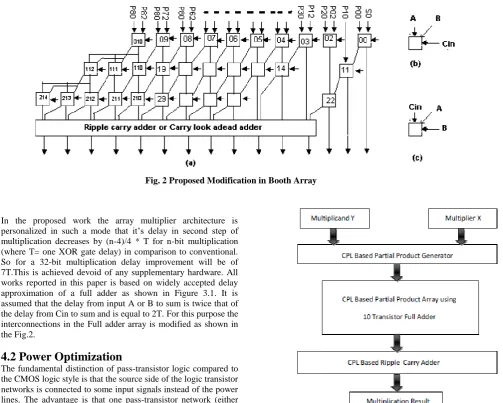
[image:2.595.74.283.355.549.2]In the proposed work the array multiplier architecture is personalized in such a mode that it’s delay in second step of multiplication decreases by (n-4)/4 * T for n-bit multiplication (where T= one XOR gate delay) in comparison to conventional. So for a 32-bit multiplication delay improvement will be of 7T.This is achieved devoid of any supplementary hardware. All works reported in this paper is based on widely accepted delay approximation of a full adder as shown in Figure 3.1. It is assumed that the delay from input A or B to sum is twice that of the delay from Cin to sum and is equal to 2T. For this purpose the interconnections in the Full adder array is modified as shown in the Fig.2.
4.2 Power Optimization
The fundamental distinction of pass-transistor logic compared to the CMOS logic style is that the source side of the logic transistor networks is connected to some input signals instead of the power lines. The advantage is that one pass-transistor network (either NMOS or PMOS) is adequate to perform the logic operation, which results in a minor number of transistors and minor input loads, especially when NMOS networks are used.
The schematic diagram of the CPL full adder circuit is shown in Fig 4.. The advantages [10], of pass logic transistors include – Smaller number of transistors and smaller input loads, along with MUX and especially XOR circuits being implemented efficiently. The shortcoming [10], of pass transistor logic is that threshold voltage drops through the NMOS transistors makes it obligatory to sustain output voltage level; hence inverter is used at output which increases the number of transistors. All the components in the Multiplier including the Booth Encoders are designed in the CPL logic.
5.
DESIGN AND ANALYSIS
5.1 Design of Full Adders
Full adders in Standard Logic Styles obtained from the literature have been designed. It shows that the CPL Based 10 T Full adder and Transmission gate 14T Full adder are the most efficient and promising ones in their Performance and Lower Power Consumption. However, the Conventional CMOS Full adder also considered here for the comparison rationale.
Another significant area which leads to the Power consumption and Delay overhead in the multiplier design is the Basic Logic gates and half adders used in it. Since we are using the Full adders in three logic styles namely Static CMOS, Transmission Function, Complementary Pass Transistor, all the basic Gates are designed in these three logic styles and the Power consumption is compared. Designing the whole circuit in a single Logic style will provide a regular layout and less area, which is essential in the design of multipliers are DSP ICs, because of the rapid growth of Personal Assistant Devices and the multimedia applications in it.
5.2 Design of Booth Encoder and Partial
Product Generators
[image:3.595.53.557.101.504.2]Various designs and its drawbacks are discussed in [5]. In the same paper they have proposed a superior encoder design which is widely accepted for the design of Booth Multipliers. Diverse
[image:3.595.328.554.104.520.2]sign extension Schemes are discussed in [4] for regular partial product array. However, Wen Chang [5] Modified Booth Encoder is the widely accepted one due to the reduction in the partial Product array. Hence the Wen Chang Booth Encoder is designed and the power consumption is analyzed.
The key point in power reduction of the Proposed Modified Booth multiplier is the CPL based Booth Encoder. The proposed Booth encoder provides best performance in terms of Power, Delay and Transistor count when comparing with other Implementations.
The area requirement of Booth encoder is awfully high when we are adopting the CMOS design style. Hence the Area and power consumption of the Booth Encoder will become almost equal to the Static CMOS implementation of the Baugh- Wooley Multiplier. Partial product rows are reduced to half in Modified Booth Encoded Multiplier, when comparing with the Baugh-Wooley multiplier. However, if we are not optimizing the area and Power consumption of the Partial Product generators, then the area and power advantage will be faded. CPL Based Enoder is shown in Fig.5
The Partial Product generator with Sign Correction Bit and Row LSB term is designed in all the three logic styles. The Negate bit is designed separately and the added to the LSBof each partial product. The sign correction is done in the modified Booth Encoder Scheme.
5.3 Design of Baugh Wooley Multiplier
Baugh-Wooley multiplier [13-15] is also an array multiplier but can perform signed multiplication. But, they are not apt for large size operands. The Baugh-Wooley algorithm [14] is a dissimilar scheme for signed multiplication, but is not so widely adopted because it may be complicated to deploy on irregular reduction trees. In our results, we have designed the Baugh-Wooley multiplier mainly to compare the area of the CMOS design of the proposed architecture. Fig. 6 shows the Proposed Multiplier
[image:4.595.64.293.78.311.2]All the designs are carried out in the Tanner EDA v.13 tool. Results are compared at 5V, 50Mhz, using 125nm technology file.
Fig. 4 CPL Based 10T Full Adder
[image:4.595.336.518.92.402.2]Fig. 5 CPL Based Modified Booth Encoder-Decoder
[image:4.595.314.552.454.672.2]6.
RESULTS AND DISCUSSIONS
Figure 5.1 shows the comparison of different full adder architectures based on the power consumption at 5V power supply. If we are not considering the delay, 17T full adder and 10 T full adders are the two architectures, which give low power consumption. However the 17 T Full adders cause severe delay problem in the cascaded circuits [13]. Hence only conventional, 14T and 10 T are considered for the analysis.
[image:5.595.46.279.243.377.2]The static CMOS Encoder array is the main reason for the large area and power usage in the conventional Modified Booth multiplier. The area usage of the different encoders is given in the figure 5.4. Results show that the design of MBE in CPL reduces the area 3 fold that of the conventional design. The corresponding Power result is show in the figure 5.5.
A Method to build a faster array multiplier by delay optimized inter connection globally is discussed in [10-11]. The multiplier architecture performance in terms of delay and hardware is compared with conventional as well as recent reported one. In terms of hard ware this architecture is also better than the last reported and gives less delay for length up to 12. But the reported one gives more delay for higher bit length multiplication. A detailed analysis of all three architectures is given based on which a designer can decide to choose the precise array architecture for his multiplier as to requirement.
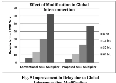
Table 2 shows the comparison of delay in the second stage of the full adder array in the conventional design and the proposed design. Graphical representation is shown in Fig.9.
From the comparison results of the multipliers it can be observed that the Array Modified Booth Multiplier is efficient in power in all the logic styles. However, when we consider the other signed multiplier like Baugh- Wooley multiplier, the MBE multiplier uses more area and consumes significant power.
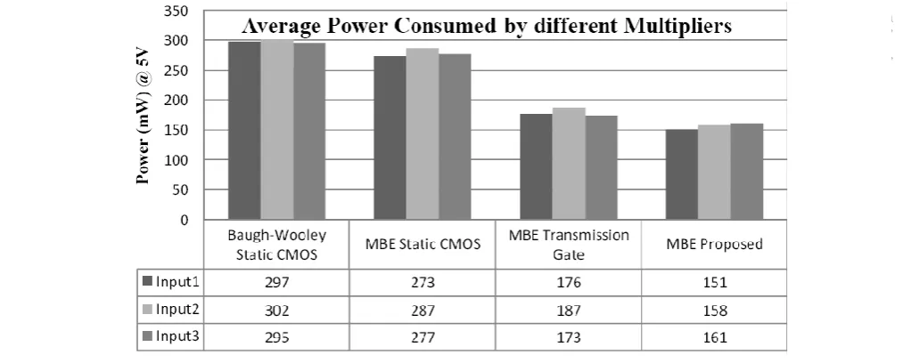
Realization of the multiplier in Transmission function logic reduces the power, however, CPL based design is the best one as the power and area are reduced by half of the conventional design. Figure 5.6, Figure 5.7 and Figure 5.8 shows the area usage, power consumption and the output waveform of the proposed multiplier respectively. Power comparison of various Full Adders and the Multipliers are shown in Fig. 7 and Fig.10. The average power has been calculated for different outputs and the results are verified. However, it can be observed that the disparity in power between CPL logic and Transmission gate logic is small, and this is due to the threshold voltage effect in Complementary logic. Area usage of the Booth Encoder and the Multipliers are shown in Fig.8 and Fig.11.
0 100 200 300 400 500
Input1 Input2 Input3
P
ow
er
(
μW)
Comparison of different Full Adders
Conventional CMOS (32T) Modified Conv CMOS (20T) Transmission Function (17T) Transmission Gate (14T)Pass Transistor (10T)
Multiplier Type Conventional
MBE Multiplier
Proposed MBE
Multiplier Comparison Criteria
Delay in 2nd Step
of multiplication
(n/2 – 1) x 2T {(3n-4 )/4}x T
0 10 20 30 40 50 60 70
Conventional MBE Multiplier Proposed MBE Multiplier
D e la y i n te rms o f XOR Ga te
Effect of Modification in Global Interconnection 8 bit 16 bit 32 bit 64 bit 0 1000 2000 3000 4000 Baugh-Wooley Using Static CMOS
MBE Using Static CMOS MBE Using Transmission Gate MBE Using Complementary Pass Transistor # Tr an si sto rs
[image:5.595.308.555.245.421.2]Comparison of area usage in different multipliers
[image:5.595.54.285.416.561.2]Fig. 7 Power comparison of various Full Adders
Fig. 8 Transistor Requirement for 1 bit Partial Product generator in various logic styles
Fig. 9 Improvement in Delay due to Global Interconnection Modification
[image:5.595.310.546.571.729.2]7.
CONCLUSION AND FUTURE WORK
The work can be extended for Higher Radix Booth multipliers reported so far and the global interconnection amendment can be checked with the compressor based Modified Booth design also. Pipelining and Truncation are not considered here for the analysis. A combination of these methods with the CPL design can obtain more efficient and promising design for the DSP Applications. Implementation of more sophisticated design in sign extension and Row LSB of MBE scheme can provide more efficient multiplier with regular layout and optimum interconnections.
8.
REFERENCES
[1] A.D. Booth,“A signed binary multiplication technique,” Quarterly Journal of Mechanics and Applied Mathematics, vol. 2, pp. 236-240, 1951.
[2] O.L.MacSorley, “High-speed arithmetic on binary computers,” IRE Transaction on Electronic Computers, vol. 49, pp. 67-91, 1961.
[3] A. R. Cooper, “Parallel Architecture Modified Booth Multiplier”, Proceedings of the Institution of Electrical Engineers, 1989.
[4] J. Fadavi-Ardekani, “M × N booth encoded multiplier generator using optimized Wallace trees,” IEEE Trans. Very Large Scale Integr. (VLSI) Syst., vol. 1, no. 2, pp. 120– 125, Jun, 1993.
[5] W.-C. Yeh and C.-W. Jen, “High-speed booth encoded parallel multiplier design,” IEEE Trans. Comput., vol. 49, no. 7, pp. 692–701, Jul, 2000.
[6] Ayman A. Fayed, Magdy A. Bayoumi, “A Novel Architecture for Low-Power Design of Parallel Multipliers," vlsi,pp.0149, IEEE Computer Society Workshop on VLSI 2001.
[7] Razaidi Hussin, Ali Yeon Md. Shakaff, Norina Idris1, Zaliman Sauli1, Rizalafande Che Ismail1 and Afzan Kama An Efficient Modified Booth Multiplier Architecture, International Conference on Electronic Design, 2008.
[8] Shiann-Rong Kuang and Jiun-Ping Wang “Modified Booth Multipliers with a Regular Partial Product Array” IEEE Transactions on Circuits and Systems—II Volume.56, No.5, 2009.
[9] Soojin Kim and Kyeongsoon Cho, “Design of High-speed Modified Booth Multipliers Operating at GHz Ranges,” World Academy of Science, Engineering and Technology, Vol. 7, No. 2, 2010.
[10] S.K. Sahoo and C. Shekhar, "A fast final adder for a 54-bit parallel multiplier for DSP application",international journal of electronics, vol. 98, no. 12, pp. 1625-1638, 2011.
[11] S.K. Sahoo and C. Shekhar,“Delay Optimized Array Multiplier for Signal and Image Processing”, 2011 International Conference on Image Information Processing, 2011.
[12] C.Senthilpari “A low power and High performance Radix-4 Multiplier design using a Modified Pass Transistor Logic Technique” IETE Journel of Research Vol. 57, Issue 2, 2012.
[13] Neil.H.Weste and Kamran Eshraghian, “Principles of CMOS VLSI Design,” Addison-Wesley, ISBN 0201733897,pp 361-380, 1993.
[14] Kiat-Seng Yeo and Kaushik Roy, “Low-Voltage,Low-Power VLSI Subsystems” Tata McGraw-Hill,ISBN-13-978-0-07-067750-0, pp 119- 146, 2009.
[15] K .Roy and S.C. Prasad, “Low Power CMOS VLSI Circuit Design,” Wiley, 2009.
AUTHOR’S PROFILE
Sajan P Philip has received B. Tech degree in Electronics and Communication from College of Engineering, Chengannur, Kerala, affiliated to Cochin University of Science and T echnology (2010). Currently his pursuing his Masters in Applied Electronics at Bannari Amman Institute of Technology, Tamil Nadu affiliated to Anna University Chennai. His research interest includes Computer Architecture, Computer Networks and VLSI Design.
[image:6.595.40.547.68.272.2]pursuing P.hd in Low Power VLSI Design under Anna University Chennai. His research interest includes Network analysis and Synthesis and Low power VLSI Design.
Dr. S Valarmathy has received BE degree in Electronics and Communication from Bharathiar University, Coimbatore, Tamil Nadu (1989). She received her ME Degree in Applied Electronics from Bharathiar University, Coimbatore, Tamil Nadu(2000). She received her P.hd degree for her work in Biometrics. Currently
![Fig. 1 Wen-Chang [4] Modified Booth Encoder](https://thumb-us.123doks.com/thumbv2/123dok_us/8086485.783738/2.595.74.283.355.549/fig-wen-chang-modified-booth-encoder.webp)