ISSN(Online) : 2319-8753 ISSN (Print) : 2347-6710
I
nternational
J
ournal of
I
nnovative
R
esearch in
S
cience,
E
ngineering and
T
echnology
(An ISO 3297: 2007 Certified Organization)
Vol. 5, Issue 3, March 2016
Modified UPQC for Compensation Power
Quality Problems Using MLI with Modified
PWM Method
Elavarasan P1, Sathyamurthy K2
PG Scholar, Dept of EEE, Arignar Anna Institute of Science and Technology, Chennai, India1
Assistant Professor, Dept of EEE, Arignar Anna Institute of Science and Technology, Chennai, India2
ABSTRACT: The unified power quality conditioner (UPQC) is a custom power device, which mitigates voltage and
current-related PQ issues in the power distribution systems. In this project, a UPQC topology for applications with non-stiff source is proposed. The proposed topology enables UPQC to have a reduced harmonics. In this project the unified power quality conditioner (UPQC) deals with a solution to compensate the voltage sags and swells and to protect sensitive load In order to apply the MLI in the distribution systems with voltage in range of kilovolts, series converter as one of the important components of UPQC should be implemented based on the multilevel converters which have the capability to handle voltage in the range of kilovolts and power of several megawatts. So, in this project a configuration of UPQC based on asymmetrical cascade Multicell converter is proposed. The main property of this asymmetrical CM converter is increase in the number of output voltage levels with reduced number of switches. Also, the pre-sag compensation strategy and the proposed voltage sag/swell detection .
KEYWORDS: FACTS, SSSC,SVC, IPFC, CSC, UPFC, UPQC, STATCOM.
I. INTRODUCTION
ISSN(Online) : 2319-8753 ISSN (Print) : 2347-6710
I
nternational
J
ournal of
I
nnovative
R
esearch in
S
cience,
E
ngineering and
T
echnology
(An ISO 3297: 2007 Certified Organization)
Vol. 5, Issue 3, March 2016
topology avoids the voltage balancing of the capacitor, but the independent control of the inverter legs is not possible. To overcome the problems associated with the four-leg topology, the authors proposed a T-connected transformer and three-phase VSC-based DSTATCOM. However, this topology increases the cost and bulkiness of the UPQC because of the presence of extra transformer. In conventional 11 levels multi-level inverter is implemented but harmonics is injected. So, we have implement 15 level in proposed system.
II.LITERATURE SURVEY
The unified power quality conditioner (UPQC) is a custom power device, which mitigates voltage and current-related PQ issues in the power distribution systems. In this project, a UPQC 15 level MLI topology for applications with non-stiff source. This project deals with a dynamic voltage restorer (UPQC 15 MLI) as a Solution to compensate the voltage sags and swells and to protect sensitive loads. Multilevel converters are very interesting alternatives for medium and high-power applications. Here we developed an improved configuration of double flying capacitor Multicell (DFCM) converter. The benefits of this new converter comparing with conventional DFCM, are doubling of the number of output voltage levels and improving the output voltage frequency spectrum.Multilevel converters are very interesting alternatives for medium and high-power applications. Here we developed an improved configuration of double flying capacitor Multicell (DFCM) converter. The benefits of this new converter comparing with conventional DFCM, are doubling of the number of output voltage levels and improving the output voltage frequency spectrum.
III. PROJECT DESCRIPTION
To reduce harmonics of circuit, we have implemented 15 level MLI is applied.
Fig. 1 Normal Pwm method with 8 switches for 11 level inverter
PROPOSED SYSTEM
1. Modified Pwm method with 10 switches for 15 level inverter.
ISSN(Online) : 2319-8753 ISSN (Print) : 2347-6710
I
nternational
J
ournal of
I
nnovative
R
esearch in
S
cience,
E
ngineering and
T
echnology
(An ISO 3297: 2007 Certified Organization)
Vol. 5, Issue 3, March 2016
Fig 2 Block diagram
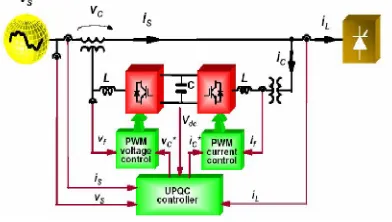
A Unified Power Quality Conditioner (UPQC) is a device that is similar in construction to a Unified Power Flow Conditioner (UPFC). The UPQC, just as in a UPFC, employs two voltage source inverters (VSIs) that connected to a D.C. energy storage capacitor. One of these two VSIs is connected in series with A.C. line while the other is connected in shunt with the A.C. system.
A UPQC that combines the operations of a Distribution Static Compensator (DSTATCOM) and Dynamic Voltage Regulator (UPQC 15 MLI) together.
One of the serious problems in electrical systems is the Increasing number of electronic components of devices that are used by industry as well as residences. These devices, which need high-quality energy to work properly, at the same time, are the most responsible ones for injections of harmonics in the distribution system. Therefore, devices that soften this drawback have been developed.
One of them is the unified power quality conditioner (UPQC), It consists of a shunt active filter together with a series-active filter. This combination allows a simultaneous compensation of the load currents and the supply voltages, so that compensated current drawn from the network and the compensated supply voltage delivered to the load are sinusoidal, balanced and minimized. The series- and shunt-active filters are connected in a back-to-back configuration, in which the shunt converter is responsible for regulating the common DC-link voltage.
Fig. 3 General Configuration of the Unified Power Quality Conditioner
AUPQCis employed in a power transmission system to perform shunt and series compensation at the same time. A power distribution system may contain unbalance, distortion and even D.C. components. Therefore aUPQCoperate, better Than a UPFC, with all these aspects in order to provide shunt or series compensation.
ISSN(Online) : 2319-8753 ISSN (Print) : 2347-6710
I
nternational
J
ournal of
I
nnovative
R
esearch in
S
cience,
E
ngineering and
T
echnology
(An ISO 3297: 2007 Certified Organization)
Vol. 5, Issue 3, March 2016
FIG. 4 Equivalent Circuit For UPQC
Taking the load voltage, VL as a reference phasor and suppose the lagging power factor of the load is CosφLwe can write;
= ∠0
= ∠ − = (1+k)∠0
Where factor k represents the fluctuation of source voltage, defined as, K=
The voltage injected by series APF must be equal to, = - =-k ∠0
The UPQC is assumed to be lossless and therefore, the active power demanded by the load is equal to the active power input at PCC. The UPQC provides a nearly unity power factor source current, therefore, for a given load condition the input active power at PCC can be expressed by the following equations,
=
. = . .cos
(1+k). = . .cos
The above equation suggests that the source current is depends on the factor k, since φL and iLare load characteristics and are constant for a particular type of load. The complex apparent power absorbed by the series APF can be expressed as,
= . ∗
= . .cos =-k. . .cos
= . .sin
φs=0, since UPQC is maintaining unity power factor
= . =-k. . =0
ISSN(Online) : 2319-8753 ISSN (Print) : 2347-6710
I
nternational
J
ournal of
I
nnovative
R
esearch in
S
cience,
E
ngineering and
T
echnology
(An ISO 3297: 2007 Certified Organization)
Vol. 5, Issue 3, March 2016
The current provided by the shunt APF, is the difference between the Input source current and the load current, which includes the load Harmonics current and the reactive current. Therefore, we can write;
= -
= ∠0 - ∠-
= -( .cos - .sin )=( - . cos )+ . sin
= . .cos = . .sin
= . . sin = . .sin
Based on the above analysis the different modes of operation are discussed
a) No UPQC b) With Shunt APF
Fig. 5 Reactive Power Flow
The reactive power flow during the normal working condition when UPQC is not connected in the circuit is shown in the Fig.(a). In this condition the reactive power required by the load is completely supplied by the source only. When the UPQC is connected in the network and the shunt APF is put into the operation, the reactive power required by the load is now provided by the shunt APF alone; suchthat no reactive power burden is put on the mains. So as long as the shunt APF is ON, it is handling all the reactive power even during voltage sag, voltage swell and current harmonic compensation condition.
The series APF is not taking any active part in supplying the load reactive power. The reactive power flow during the entire operation of UPQC is shown in the Fig. (b). In this case no active power transfer takes place via UPQC, termed as Zero Active Power Consumption Mode.
If the load is a non linear one producing harmonics, in such cases the shunt APF injects current equals to the sum of harmonics current but in opposite direction, thus cancelling out any current harmonics generated by non linear load. During this current harmonics compensation mode of operation them shunt APF does not consume any real power from the source since it injected only harmonics currents. Here
Phasor represents the normal working condition, considering leading power factor angle of the load. During this condition iSwill be exactly equal to the iL. When shunt APF is put into the operation, it cancels out the vars generated by load by injecting a 900 lagging current such that the source current will be in phase with the terminal voltage. The phasor representing this inductive effect is shown in Fig.3.8 the phasor representations during voltage sag and voltage swell condition on the system are shown in the Fig.3.9 and Fig. 3.10 respectively.
ISSN(Online) : 2319-8753 ISSN (Print) : 2347-6710
I
nternational
J
ournal of
I
nnovative
R
esearch in
S
cience,
E
ngineering and
T
echnology
(An ISO 3297: 2007 Certified Organization)
Vol. 5, Issue 3, March 2016
IV. CIRCUIT TOPOLOGY
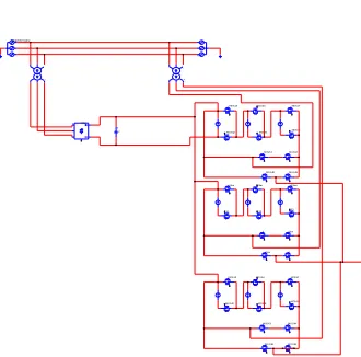
Fig. 6 Proposed Inverter Circuit
A typical UPQC 15 MLI for voltage sag/swell compensation is shown in Fig. 4. 1. When the supply-side voltage changes the UPQC 15 MLI injects a series voltage to maintain the magnitude of the load voltage at its reference value. The UPQC 15 MLI is essentially a voltage-source converter that produces an ac output voltage and injects it in series with the supply voltage. Note that the voltage injection also results in the supply or absorb of active and reactive power. Reactive power can be supplied without taking energy from the dc-side capacitor; however, an active power supply must involve the exchange of stored energy.
The series converter consists of a three-phase voltage-source converter or three single-phase voltage-source converters. It starts to inject three single-phase compensating voltages in series into the power line as soon as voltage sag or swell occurs. In this project, asymmetrical CM converter, introduced in [3], based UPQC 15 MLI is proposed to increase the number of output voltage levels and as a result, reduce the output voltage THD and make it possible to implement UPQC 15 MLI in the distribution systems with voltage in range of kilovolts. A new 15-level asymmetrical CM converter is shown in Fig. 2. The main property of the new configuration of asymmetrical CM converter in comparison with the conventional asymmetrical CM converter is reduction in the number of required high-frequency switches by 50 percent while only 4 low-frequency switches are added. As a result, the cost, size and the power loss of the new configuration of asymmetrical CM converter is decreased. The configuration of UPQC 15 MLI based on configuration of 15-level asymmetrical CM converter is shown in Fig. 4.1.
CONTROL STRATEGIES
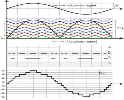
Asymmetrical Cascade Multicell Converter Control Strategy The mentioned configuration of asymmetrical CM converter is controlled by level shifted sinusoidal pulse width modulation (LS-SPWM), as shown in Fig. 4, while the absolute of the reference signal is intersected with the level shifted triangle carriers. The low-frequency switch (Ja) is on for positive reference signal and is off for negative reference signal. All states of switches are illustrated in details in Table-I. B. Voltage Sag/Swell Compensation Strategy To avoid tripping of the load, the amplitude and phase angle of the load voltage has to be restored by the UPQC 15 MLI. Different strategies can be used to achieve this goal.
threephasesupply
V SC
C
s1bar S2bar S3bar
Jbar J
S3 S2 S1
J Jbar
MOS35 MOS36 MOS37
MOS38 MOS39
MOS40 MOS41 MOS42
MOS43 MOS44
MOS45 MOS46 MOS47
MOS48 MOS49
MOS50 MOS51 MOS52
ISSN(Online) : 2319-8753 ISSN (Print) : 2347-6710
I
nternational
J
ournal of
I
nnovative
R
esearch in
S
cience,
E
ngineering and
T
echnology
(An ISO 3297: 2007 Certified Organization)
Vol. 5, Issue 3, March 2016
In this , the SRF, which is proposed in ,is used to detect the voltage sags/swells and determine the UPQC 15 MLI reference injected voltage. At the beginning, the voltage sag/swell must be detected and then, the UPQC 15 MLI reference injected voltage must be determined.
Fig. 7 Level Shifted Sinusoidal Pulse Width Modulation.
states of switches and output voltage for 15-level asymmetrical cascade Multicell converter. where, a grid V, b grid V , c grid V are the measured line-neutral grid voltages of phases a, b and c, respectively and d grid V, q grid V, 0, grid V are the d-component, q-component and zero-component of grid voltages in the SRF, respectively. Also, the rms value (line-neutral) of balanced grid voltage (grid V ) can be calculated using the d-component and q-component of grid voltages as follows:
ISSN(Online) : 2319-8753 ISSN (Print) : 2347-6710
I
nternational
J
ournal of
I
nnovative
R
esearch in
S
cience,
E
ngineering and
T
echnology
(An ISO 3297: 2007 Certified Organization)
Vol. 5, Issue 3, March 2016
Components of grid voltages in the SRF, respectively. In the case of single phase voltage sag/swell or unbalanced three phase voltage sag/swell, the zero-component of grid voltages in the SRF is not nil. Therefore, it can be used as a parameter to detect the voltage sag/swell.
However, in the case of balanced three phase voltage sag/swell, the zero-component of grid voltages in the SRF is nil and only the rms value of balanced grid voltage in the sag/swell state changes. Because of that, it is necessary to use the rms value of line-neutral grid voltages (grid V ) obtained from (2) as another parameter to detect the voltage sag/swell. Finally, the following proposed algorithm based on two steps is performed iteratively to detect the voltage sag/swell: Step-1: The zero-component of grid voltages in the SRF which is obtained from (1) is analyzed.
If it is not equal zero, it means that the unbalanced voltage sag/swell is occurred. So, the voltage sag/swell is detected and then, exit the algorithm. If the zero component is equal to zero, go to step-2. The nil zero-component means that the grid voltages are balanced. So, the rms value of grid voltages must be analyzed as step-2. Step-2: The rms value of line-neutral grid voltages (grid V ) obtained from (2) is compared with the reference rms value of line-neutral grid voltages ( ref rms V ). If they are not equal to each other, it means that the voltage sag/swell is occurred. So, the voltage sag/swell is detected and then, exit the algorithm.
If there is no difference between them, go to step-1. Using the balanced or unbalanced voltage sag/swell. After the detection of voltage sag/swell, the reference rms value of line-neutral grid voltages (ref rms V ) and
the obtained reference angle (ref θ ) are used to determine the values of reference grid voltages in the SRF as follows:
ISSN(Online) : 2319-8753 ISSN (Print) : 2347-6710
I
nternational
J
ournal of
I
nnovative
R
esearch in
S
cience,
E
ngineering and
T
echnology
(An ISO 3297: 2007 Certified Organization)
Vol. 5, Issue 3, March 2016
V. SIMULATION RESULTS
Fig. 8 Simulation Circuit Diagram
Fig.9Input Sag Voltage of Proposed Method
Fig. 10 Input Sag Current of Proposed Method IN PUT VO LTAGE
G RID
ABC
+
-three phase inverter
-K-rmsi -K-rms D iscret e,
Ts = 5e- 005 s.
powergui Con n1 Con n2 Con n3 load A1 B1 C1 A2 B2 C2 A B C
injected trans former 1
v + -Va bc Ia bc A B C a b c Vab c Iab c A B C a b c Th ree-Phase V -I Measur emen t
ABC
abc Three-P hase Transformer (Two Windings)2 A B C A B C Th ree-Phase Ser ies R LC B ra nch1 N
A B C Thr ee-P hase Pr ogra mma ble Voltag e S ource
SOU RCE V4
Vab c
Iab c Ma g _V_I
P_Q PQ &VI5 Va bc
Ia bc Ma g_ V_I
P_ Q Va bc
Ia bc Ma g_ V_I
P_ Q
1
2
1
2
Lin ear Tran sform er 21
2
Lin ear Tra nsfor mer 1
ABC ABC Lf4
ABC
ABC
Lf3 A B C A B C Lf1
ABC
ABC
Lf A B C A B C Cf VabcIabc
A BabCc
A B C a b c B4
ABC
abc B 3
ABC
abc B1
A C DC
-B DC
+
15 LEVE L A SYMME RICAL CM CONV ERTER
0 0.1 0.2 0.3 0.4 0.5 0.6 0.7
-2 -1.5 -1 -0.5 0 0.5 1 1.5
2x 10
4 Time(sec) V o lt a g e (V )
0 0.1 0.2 0.3 0.4 0.5 0.6 0.7
ISSN(Online) : 2319-8753 ISSN (Print) : 2347-6710
I
nternational
J
ournal of
I
nnovative
R
esearch in
S
cience,
E
ngineering and
T
echnology
(An ISO 3297: 2007 Certified Organization)
Vol. 5, Issue 3, March 2016
FIG.6.4 COMPENSATED SAG VOLTAGE OF PROPOSED METHOD
FIG.6.5 COMPENSATED SAG CURRENT OF PROPOSED METHOD
FIG.6.6 SAG PFC OF PROPOSED METHOD
FIG.6.7 MLI OF PROPOSED METHOD
0 0.1 0.2 0.3 0.4 0.5 0.6 0.7 -4
-3 -2 -1 0 1 2 3 4x 10⁴
Time
c
om
p
en
sa
te
V
o
lta
ge
(V
)
0 0.1 0.2 0.3 0.4 0.5 0.6 0.7
-800 -600 -400 -200 0 200 400 600 800
Tim e(sec)
C
ur
re
n
t(
I)
0 0.1 0.2 0.3 0.4 0.5 0.6 0.7
-2.5 -2 -1.5 -1 -0.5 0 0.5 1 1.5 2 2.5x 10⁴
Time(sec)
P
F
C
0 0.1 0.2 0.3 0.4 0.5 0.6 0. 7 -8000
-6000 -4000 -2000 0 2000 4000 6000 8000
Time(sec)
M
ISSN(Online) : 2319-8753 ISSN (Print) : 2347-6710
I
nternational
J
ournal of
I
nnovative
R
esearch in
S
cience,
E
ngineering and
T
echnology
(An ISO 3297: 2007 Certified Organization)
Vol. 5, Issue 3, March 2016
FIG.6.8 MLI CIRCUIT OF PROPOSED METHOD
FIG.6.9 SWELLS VOLTAGE OF PROPOSED METHOD
FIG.6.10 SWELL CURRENT OF PROPOSED SWELL METH
FIG.6.11 COMPENSATE VOLTAGE OF PROPOSED SWELL METHOD
ja ja ja1 ja 1 S1 S 11 S2 S3 S3 1 S 21 ja ja ja 1 ja 1 S1 S11
S2 S 3
S3 1 S2 1 ja ja ja1 ja1 S 1 S1 1
S 2 S3
S31 S2 1
5 D C -4 D C +
3 C 2 B 1 A v + -v + -v +
-sine wav es 3 s33 S u bsystem 8 sin e wav es2s22 S u bsystem 7 sin e wav e
s1 s11 S u bsystem 6 sine w av es11s1
S ub syste m 5 sine wav es22s2
S ub syste m 4 sine wav eS ub syste m 3s33s3 sine w ave s1
s11 S ubsyste m2
sine w ave s2 s22 S ub syste m1
sine w ave s3 s33 S ub sy ste m
S in e Wa ve4 S ine Wave 1 S ine Wave > =
Rel ati on al O pe rat or7
> = Rela tio na l Op er ato r2 >= Re lat ion al Ope ra tor 1
NOT NOT NOT gm CE gm CE gm CE g m C E gm CE g m C E gm CE g mC E gm CE gm CE g m C E gm CE g m C E g mC E gm CE gm CE gm CE gm CE gm CE gm CE gm CE g mC E gm CE g mC E g m C E gm CE gm CE gm CE gm CE gm CE 0 Co nsta nt2 0 Con stan t1 0
Con stan t
0 0.1 0.2 0.3 0.4 0.5 0.6 0.7
-4 -3 -2 -1 0 1 2 3 4x 10
ISSN(Online) : 2319-8753 ISSN (Print) : 2347-6710
I
nternational
J
ournal of
I
nnovative
R
esearch in
S
cience,
E
ngineering and
T
echnology
(An ISO 3297: 2007 Certified Organization)
Vol. 5, Issue 3, March 2016
FIG.6.12 COMPENSATE CURRENT OF PROPOSED SWELL METHOD
FIG.6.13 EXISTING CIRCUIT DIAGRAM
FIG.6.14 EXISTING THD VALUE
0 0.1 0.2 0.3 0.4 0.5 0.6 0.7
-800 -600 -400 -200 0 200 400 600 800 Time(sec) C o m p e n sa te (C u rre nt) k S2 s1 J k S2 k S2 sag Di scre te ,
T s = 2 e -0 05 s.
p o werg u i
A B C + -non linear load
A1 B1 C1 A2 B2 C2 A B C
in ject ed tra nsfor me r
N A B C V oltage Source
v +-V1 V g A B C + -A B C A B C
ABC abc
Va b c Ia b c A B C abc Vab c I ab c A B C a bc Vab c
I ab c A B C a bc
ABC abc
A B C A B C Out1 Sub syste m6 Out1
Sub syste m5
Out1 Sub syste m4 Out1
Sub syste m3
Out1 Sub system 2 Out1
Sub syste m1 VA
VA 1
VA 2 SE R IES PU LS E
sag detec
sag detec pulse
Sub syste m
Sco pe 6
Scop e3 Sco pe 2
Scop e1 Scop e
SO URCE VSOURCE I
RL 3 RL 2 1 2 1 2 1 2 A B C A B C L f3 A B C A B C L f2
A BC A BC
Lf
INJECT ED VO LT AGE AND CURRENT
g C E g C E g C E g C E g C E g C E g C E g C E g C E g C E g CE g CE g C E g C E g C E g CE g C E g
C E g C E g C E g CE g C E g C E g CE I 2 I
DC Voltage
A B C A B C Cf B reaker2 Breaker1 B reaker
VabcAIabcBabCcB3
Vabc Iabc A Ba bCc
B2 VabcAIabcBabCcB1
NOT9
NO T
8 7NOT
NOT 6
NO T
5 4NOT
a bc M a g P h a se a b cM ag
P h a se
NOT3
NOT
2 1NOT
v 2 v 1 NO T 2 NO T 1 NO T v
+-0 0.1 0.2 0.3 0.4 0.5 0.6 0.7 -5
0 5
Selected signal: 35 cycles. FFT window (in red): 3 cycles
Time (s)
0 200 400 600 800 1000
0 5 10 15 20 25 30 Frequency (Hz) Fundamental (50Hz) = 0.9434 , THD= 29.82%
ISSN(Online) : 2319-8753 ISSN (Print) : 2347-6710
I
nternational
J
ournal of
I
nnovative
R
esearch in
S
cience,
E
ngineering and
T
echnology
(An ISO 3297: 2007 Certified Organization)
Vol. 5, Issue 3, March 2016
FIG.6.15 PROPOSED THD VALUE
VI. CONCLUSION
Voltage sags/swells are major problems in power systems due to the increased integration of sensitive loads into them. UPQC 15 MLI systems are able to compensate these voltage sags/swells.Because the multi cell converters are very interesting for high-power/medium-voltage applications, and also considerably improve the output voltage frequency spectrum, in this project configuration of UPQC 15 MLI based on asymmetrical CM converter has been proposed to improve the quality of UPQC 15 MLI output voltage and to be used in the distribution systems with voltage in range of kilovolts. In the proposed configuration of UPQC 15 MLI, number of required high-frequency switches is reduced by 50 percent.
Therefore, the cost, size and power loss are decreased. Also, new methods based on the SRF have been used to detect the voltage sag/swell and determine the reference series injected voltage of UPQC 15 MLI. As depicted in simulation results, the pre-sag compensation strategy and the proposed SRF based detection and determination methods show excellent performance and good dynamic response time.
REFERENCES
[1] “Performance Analysis of Improved Double Flying Capacitor Multicell Converter”, Amal Philomiya L1, Saravanan.C2, Narasimman.P,International Journal of Emerging Technology and Advanced Engineering,(ISSN 2250-2459, ISO 9001:2008 Certified Journal, Volume 3, Issue 7, July 2013).
[2] “A Modified Three-Phase Four-Wire UPQC Topology With Reduced DC-Link Voltage Rating”, Srinivas BhaskarKaranki, NageshGeddada, IEEE transactions on power electronics, vol. 23, no. 6, November 2008
[3] ”Voltage Sag and Swell Compensation with UPQC 15 MLI Based on Asymmetrical Cascade Multicell Converter “,S. MasoudBarakati,IEEE transactions on power delivery, vol. 23, no. 2, April 2008.
[4]“Performance Analysis of Improved Double Flying Capacitor MulticellConverter”,AmalPhilomiya, Saravanan., Narasimman,ESEVIER11 September 2006..
[5] M.R.Banaei, S.H.Hosseini, S.Khanmohamadia and G.B.Gharehpetian, “Verification of a new energy control strategy for dynamic voltage restorer by simulation”, Elsevier Journal of Simulation Modeling Practice and Theory, vol. 14, no. 2, pp. 112–125, Feb. 2006.
[6] S.H. Hosseini, A.KhoshkbarSadigh and G. Gharehpetian, “Flying capacitor multicell converter based DVR with energy minimized compensation strategy”, in Proc. of 6th Int. Conf. ELECO, Nov. 2009, Bursa, Turkey, pp. 1–5.
[7] S.H. Hosseini, A. KhoshkbarSadigh and A. Sharifi, “Estimation of flying capacitors voltages in multicell converters”, in Proc. 6th International Conference ECTI-CON, Pattaya, Thailand, May 2009, pp. 110–113.
[8] A.KhoshkbarSadigh, E.Babaei, S. H.Hosseini and M. Farasat, “Dynamic voltage restorer based on stacked multicell converter”, in Proc. of ISIEA, Oct. 2009, Kuala Lumpur, Malaysia, pp. 1–6. [9] A. KhoshkbarSadigh, S. H. Hosseini, S. M. Barakati and G. Gharehpetian, “Flying capacitor multicell converter based dynamic voltage restorer”, in Proc. of 41st NAPS, Oct. 2009, Mississippi State, USA, pp. 1–6.
[9]A.KhoshkbarSadigh, S.H. Hosseini, S.M. Barakati and G. Gharehpetian, “Stacked multicell converter based DVR with energy minimized compensation strategy”, in Proc. of 41st NAPS, Oct. 2009, Mississippi State, USA, pp. 1–6.
[10]C.S.Lam, M.C.Wong and Y.D.Han, “Voltage swell and over-voltage compensation with unidirectional power flow controlled dynamic voltage restorer”, IEEE Trans. Power Delivery, pp. 2513–2521, Oct. 2008.
0 0.1 0.2 0.3 0.4 0.5 0.6 0. 7
-500 0 500
Selected signal: 35 cycles. FFT window (in red): 3 cycles
Time (s)
0 200 400 600 800 1000
0 5 10 15 20 25
Frequency (Hz)
Fundamental (50Hz) = 398. 7 , THD= 6.15%
M
a
g
(
%
o
f
F
u
n
d
a
m
e
n
ta
ISSN(Online) : 2319-8753 ISSN (Print) : 2347-6710
I
nternational
J
ournal of
I
nnovative
R
esearch in
S
cience,
E
ngineering and
T
echnology
(An ISO 3297: 2007 Certified Organization)
Vol. 5, Issue 3, March 2016
[11]J. Lamoree, L. Tang, C. DeWinkel, and P. Vinett, “Description of a micro-SMES system for protection of critical customer facilities”, IEEE Trans. Power Delivery, vol. 9, no. 2, pp. 984–991, Apr. 1994.
[12]S.A. Saleh, C. R. Moloney and M. A. Rahman, “Implementation of a dynamic voltage restorer system based on discrete wavelet transforms”, IEEE Trans. Power Delivery, vol. 23, no. 4, pp. 2366–2375, Oct. 2008.
[13]P.R.Sánchez, E.Acha, J. E. O. Calderon, V. Feliu and A. G. Cerrada, “A Versatile control scheme for a dynamic voltage restorer for power-quality improvement”, IEEE Trans. Power Delivery, vol. 24, no. 1, pp. 277–284, Jan. 2009.
[14]B.Wang and G.Venkataramanan, “Dynamic voltage restorer utilizing a matrix converter and flywheel energy storage”, IEEE Trans. Industry Applications, vol. 45, no. 1, pp. 222–231, Jan./Feb. 2009.