A Simulation Analysis of Grid Synchronized
H-Bridge Multilevel Inverter with PV Module – An
Open Loop Study
Vimal Patel
1, Darshan Vora
2PG Student [PS], Dept. of EE, CGPIT, Bardoli, Gujarat, India1,
Assistant Professor, Dept. of EE, CGPIT, Bardoli, Gujarat, India2
ABSTRACT:In the power generation sector, Natural Resources like Solar, Wind, Tidal, Geothermal, Hydro etc have always played a very important role. Out of these solar PV (photo voltaic) is most popular due to its significant advantages. However the solar radiation never remains constant. It keeps on varying throughout the day. In this paper, single 60 W solar PV panel along with boost converter have been interfaced and control for a three phase three-level neutral point clamped inverter (NPC) for grid connected photovoltaic (PV) system. The need of the hour is to deliver a constant voltage to the grid irrespective of the variation in temperatures and solar isolation. The maximum power point tracking (MPPT) is capable of extracting maximum power from the photovoltaic (PV) array connected to each DC link voltage level. The MPPT algorithm is solved by Perturb & Observe method. We have designed a circuit such that it delivers constant and stepped up dc voltage to the load. We have studied the open loop characteristics of the PV array with variation in temperature and irradiation levels. Then we coupled the PV array with the boost converter in such a way that with variation in load, the varying input current and voltage to the converter follows the open circuit characteristic of the PV array closely. At various isolation levels, the load is varied and the corresponding variation in the input voltage and current to the boost converter is noted. It is noted that the changing input voltage and current follows the open circuit characteristics of the PV array closely.
KEYWORDS: Three phase three-level cascaded H-Bridge inverter, Multilevel inverter, Grid connected, Photovoltaic, Maximum power point tracking (MPPT), boost converter, grid connection.
I. INTRODUCTION
In recent years, there has been an increasing interest in electrical power generation from renewable-energy sources, such as photovoltaic (PV) or wind-power systems. The benefits of power generation from these sources are widely accepted.
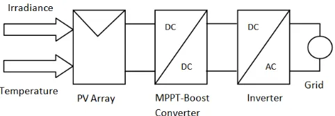
Figure 1 Grid Connected PV system block diagram
PV array convert sun energy into DC power. In practice, PV array is connected to a maximum power point tracker (MPPT) in order to convert the PV array to maximum power. The produced DC power is then converted into AC power using inverter before delivered into the utility grid.
The grid inverter is different from a typical inverter that used in stand-alone PV system. The main specification of the grid inverter is that current drawn from the inverter is delivered to the utility grid at unity power factor. Various studies on modeling PV system components show that it has become increasingly important in the PV system development. By modeling PV system using simulation software, the system could be evaluated and analyzed without adjusting the real system and this is major saving in cost and time.
This work will focus on the inverter modeling for open loop operation and boost converter design, which is a part of the development of a complete system simulation model.
II. PV ARRAY SIMULATION MODEL
Photovoltaic array output is nonlinear and there’s a correlation between the output power, light intensity and environmental temperature. The PV cells terminal voltage changes according to light intensity and environment temperature, so the output power is changed. For PV modelling, equation for m-file programming is given below:
= + + +
where I is the PV cells terminal current when full light is available, Iph is photocurrent, ID1 and ID2 are the current
through the diodes, respectively, Ipis the leakage current.
= +
= (exp ( + ) −1)
= (exp ( + ) −1)
where V is the PV cells terminal voltage when light is shone on them, is the equivalent series resistance, is the
equivalent parallel resistance, and are the diode reverse saturation current, A is diode ideality factor, q is the
electronic charge, k is the disposal of Boltzmann's constant, T is the temperature, E is the solar radiation intensity, is
The number of series cells, is the number of shunt cells.
Substituting the three equations into main equation establishes the equation as:
= − exp ( + ) −1
− exp + −1 − +
The solar cells terminal current of the PV array can be expressed as
= { − exp
+
− exp
+
−1
−
+ ( )
}
Some parameters in the above formula are shown as:
= (1 + )
= exp( )
= / exp( )
= +
= + +
= exp( )
Where, =−5.729 10 , = 0.1098, = 44.535, =−1.264 10 , = 11.800, =−7.317 10 , =
2.000, = 0, = 1.070, = 1.613 10 , =−4.470 10 , = 2.303 10 , =−2.812 10
PV mismatch is an important issue in the PV system. Due to the unequal received irradiance, different temperature and aging of the PV panels, the MPP of each PV module may be different. If each PV module is not controlled individually, the efficiency of the overall PV system will be decreased.
III. MPPT ALGORITHAM
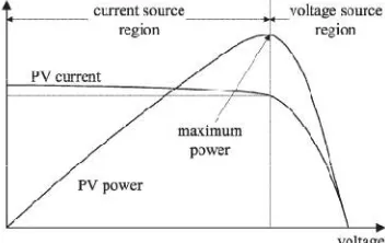
PV cell array output is nonlinear, and its output voltage and power is related with light intensity, environmental temperature and load condition. Under certain environment, the output voltage of PV cell will be different in a certain range. The output power of photovoltaic cells arrives at maximum only in a certain output voltage value, called the maximum power point. Therefore, making the PV system work at around the maximum power point is called the maximum power point tracking (MPPT).
Different MPPT algorithms were proposed, say perturb and observe method, hill climbing control method, conductance increment method, three-point comparison method, constant voltage method and so on. These principles of the algorithm differ from each other and so that the control effect is different. Among them, the perturb and observe method is widely used.
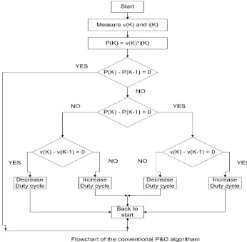
The most widely used algorithm is the Perturb & Observe (P&O) algorithm. The P&O algorithm perturbs the duty cycle which controls the power converter, in this way it takes steps over the p-v characteristic to find the MPP. This perturbation causes a new operating point with a different output power. In case this output power is larger than the previous output power, this point is set as the new operating point. In case it is lower, the same power point is adjusted to a lower or higher working voltage, depending on the previous step direction. A flowchart of the P&O algorithm is found in figure. In several studies, it has been shown that P&O has led to efficiencies as high as 96.5% in, and 99.5% in.
Figure 3 P & O algorithm flow chart
IV. BOOST CONVERTER
Boost converter is also called as the step up converter as output of Boost converter is always greater than that of the input. Figure shows the schematic diagram of Boost converter. Boost converter consists of input voltage source, switch, inductor, diode, capacitor and resistor which act as a load. The switch can be closed or open depends on the output requirement. The output voltage across the load or resistor is always greater than that of input voltage. A boost regulator can step up the voltage without a transformer. Due to a single switch, it has a high efficiency. The input current is continuous. The output voltage is very sensitive to changes in duty cycle D in equation. The average output current is less than the average inductor current by a factor of (1-D), and a much higher rms current would flow through the filter capacitor.
Figure 4 Boost converter circuit diagram
If the boost converter operates in continuous conduction mode (CCM), then the value of inductance L from the inductor current ripple analysis is given by equation given below:
= (1− ) ∗
The minimum value of filter capacitance that results in voltage ripple Vr = deltaVO/VO is given by equation:
=
∗ ∗
V. INVERTER TOPOLOGY
Early Inverters used Thyristor switches, having switching frequency a few hundred Hertz, while the present day switches like IGBT have switching frequency of several Kilohertz. Also Thyristor requires a commutation circuit while using with DC, so self commutated switches like IGBT are preferred over Thyristor. Normally electronic switches have unidirectional current carrying property; to make them bidirectional an anti-parallel diode is connected.
In general three different types of multilevel inverters are used, which are as follows -
Cascaded H Bridge Inverter
Diode Clamped Inverter
Flying Capacitor Inverter
A. Advantages & Disadvantages of H-Bridge Multi Level Inverter
Among multilevel inverter topologies Cascaded H Bridge Inverter is a modular one and simplest to control
Though it have the disadvantage of using multiple dc sources.
But it does not require extra capacitors and diodes.
The number of possible output voltage levels( ) is more than twice the number of identical DC sources or single
phase inverters( ) used
= 2 + 1
B. Advantages & Disadvantages of Diode Clamped Multilevel Inverter
Diode Clamped Multilevel Inverter has high efficiency when compared to other types, as all the switches are
fired at the fundamental frequency.
The Diode Clamped Inverter has simple firing control.
But the disadvantage of the Diode Clamped Inverter is excessive need of clamping diode.
Also the controlling of real power flow is difficult for individual block of multilevel inverter.
For controlling multilevel inverters various techniques has been proposed, among these three controlling techniques are majorly used
Sinusoidal Pulse Width Modulation (SPWM)
Selective Harmonic Elimination (SHE-PWM)
Space Vector Modulation (SVM)
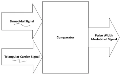
The peak magnitude of the sinusoidal signal ( ) is less than or equal to the peak magnitude of the carrier signal ( ). An important parameter of Sine PWM is modulation index
=
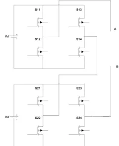
C. Configuration of Cascade Connected Single Phase H Bridge Five Level Inverter
In a Five level inverter, two, Single Phase H Bridge Inverter are connected in cascade to get five different voltage levels and is shown in Fig.4. The input dc voltage of the two, single phase module is same. If the input dc sources are
of then five level of voltage available at output are +2 , + , 0,− ,−2
The output voltage can be taken across load as , while and are output of Inverter 1 & 2 respectively. For
these five outputs voltage levels the combinations of eight switch firing is given in Table. From analysis of Table , one can realize that the two switches connected in one leg in series have firing sequence complimentary to each other.
Figure 7 5 level H Bridge inverter topology
Table 1 Switching table for 5 level CHB inverter
1 0 0 1 1 0 0 1
1 0 0 1 1 0 1 0
1 0 1 0 1 0 1 0
1 0 1 0 0 1 1 0
0 1 1 0 0 1 1 0
VI. SIMULATION RESULT
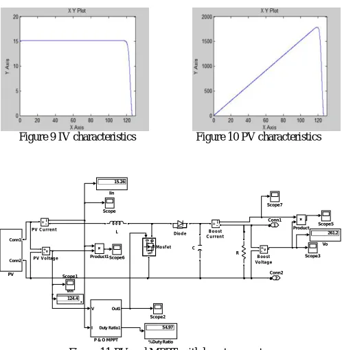
Figure 8 Modeling of PV
2 Conn2 1 Conn1
25 Te mperature
1 Suns 1000 W/m2
Scope 2
Scope 1
Scope Product
v + -PV Voltage i +-PV Current
Va Suns Ta C
Ia solar2
Embedded MATLAB Function
15.2 Display1
s -+ Controlled
Current Source
Figure 9 IV characteristics Figure 10 PV characteristics
Figure 11 PV and MPPT with boost converter
Figure 12 Full modeling of Inverter with open loop grid system
Figure 13 Voltage and current of Grid and Inverter
2 Conn2 1 Conn1 261.2 Vo 124.4 Vin Scope7 Scope6 Scope5 Scope3 Scope2 Scope1 Scope R Product1 Product v + -PV Voltage i +-PV Current Conn1 Conn2 PV V I Out1 Duty Ratio1
P & O M PPT
g D S Mosfet L 15.26 Iin Diode
C +v
-Boost Voltage i +-Boost Current 54.97
% Duty Ratio
Discrete, Ts = 5e-005 s.
powergui v + -Vo5 v + -Vo4 v + -Vo3 v + -Vo 2 v + -Vo1 Conn1 Conn2 Subsystem3 Conn1 Conn2 Subsystem1 In1 Out1 Out2 Out3 Out4 Out5 Out6 Out7 Out8 Subsystem Sine
Wave Scope 5
Scope 4 Scope3 Scope2 Scope 1 R5 R4 R3 R1 g m D S Mosfet7 g m D S Mosfet6 g m D S Mosfet5 g m D S Mosfet4 g m D S Mosfet3 g m D S Mosfet2 g m D S Mosfet1 g m D S Mosfet i +-Io Grid1 [R11] Goto7 [R21] Goto6 [R12] Goto5 [R22] Goto4 [R13] Goto3 [R14] Goto2 [R23] Goto1 [R24] Goto [R24] From9 [R22] From8 [R23] From7 [R21] From6 [R14] From5 [R12] From4 [R13] From3 [R11] From 290.8 Display1 217.3 Display InRMS Discrete RMS value1 In RMS Discrete RMS value Add 5 ohm 1 mH
1.5 1.55 1.6 1.65 1.7 1.75 1.8 1.85 1.9 1.95 2
VII. CONCLUSION
The Cascade Connected H Bridge Five level Inverter has been simulated in MATLAB and Firing pulses has been generated using two topologies Multi Carrier Sine Pulse Width Modulation. Output pulse waveform, voltage and current waveforms have been observed. Higher Order Harmonics can be removed simply using Low Pass Filter while for Lower Order Harmonics Selective Harmonics Elimination Technique need to be applied. It can be concluded that for better performance of a multilevel inverter Sine PWM Firing Technique can be implemented. For open loop control of inverter and with grid connection, ott filter is used and at the end, grid and inverter voltage and current are in phase.
REFERENCES
[1] Lakhan Kumar Gupta, K. T. Chaturvedi, “Simulation of a Cascade Connected H–Bridge Five Level Inverter,” IEEE 2014
[2] Neng Cao, Yajun Cao and Jiaoyu Liu, “Modeling and Analysis of Grid-Connected Inverter for PV Generation,” Proceedings of the 2nd International Conference on Computer Science and Electronics Engineering (ICCSEE 2013)
[3] Serkan Sezen, Engin Özdemir, “Modeling, simulation and control of three-phase three level multilevel inverter for grid connected photovoltaic system”, JOURNAL OF OPTOELECTRONICS AND ADVANCED MATERIALS Vol. 15, No.3 - 4, March – April 2013, p. 335 - 341 [4] Brigitte Hauke, “Basic Calculation of a Boost Converter's Power Stage”,Application Report November 2009–Revised January 2014
[5] Atiqah Hamizah Mohd Nordin, Ahmad Maliki Omar, Hedzlin Zainuddin, “Modeling and Simulation of Grid Inverter in Grid- Connected Photovoltaic System”, International Journal Of Renewable Energy Research, Vol. 4, No. 4, 2014