ISSN(Online): 2319-8753 ISSN (Print) : 2347-6710
I
nternational
J
ournal of
I
nnovative
R
esearch in
S
cience,
E
ngineering and
T
echnology
(A High Impact Factor, Monthly, Peer Reviewed Journal)
Vol. 5, Issue 2, Februray 2016
Low Power High Speed Performance of CLA
Using Reversible Logic
Thamu1, Santhosh2, Sudhakharan3, Suresh4
UG Student, Dept of ECE, VELTECH, Chennai, India1,2,3 Asst. Professor, Dept of ECE, VELTECH, Chennai, India4
ABSTRACT: Reversible logic is a popular concept in energy efficient computations and this will be the demand for upcoming future computing technologies. Reversible logic is emerging as an important research area and it will be having wide applications in many fields such as optical information processing, quantum computing and Low power CMOS design.The main purpose of designing reversible logic is to decrease quantum cost, depth ofthe circuits and the number of garbage outputs.Reversible are circuits (gates) that have one to one mapping between vectors ofinputs and outputs;thus the vector of inputstates can be alwaysreconstructed from thevector of output states.Reversible logic is playing a significant role in quantum computing as quantum operations are unitary in nature. Quantum computer performs computation at an atomic level; thereby doing high performance computations beyond the limits of the conventional computing systems. Reversible arithmetic units such as adders, subtractors, multipliers form the essential component of a quantum computing system. Among the adder designs, carry look-ahead is widely used in high performance computing due to its O (log n) depth. In this work, we present improved designs of both in-place and out-of-place reversible carry look-ahead adder proposed. The proposed designs utilize the properties of the Reversible Peres gate are optimize the logic depth, quantum cost and gate count compared to the existing designs proposed to both the improved designs assume no input carry (C0=0). While the first approach makes use of ancilla bits to store the sum outputs, the second approach stores the sum outputs in one of the input locations.
KEYWORDS: Reversible logic gates, Reduced garbage output, Quantum cost, Low power design, Carry look-ahead adder,Peres gate, Ancilla bits.
I. INTRODUCTION
The demand for implementing ultralow-power digital systems in many modern applications, such as mobile systems, sensor networks, and implanted biomedical systems, has increased the importance of designing logic circuits in subthreshold regime. These emerging applications have low energy as the primary concern instead of performance, with the eventual goal of harvesting energy from the environment.
The heat dissipated in the circuit will gradually decrease the performance and also life span of the circuit or device. In order to overcome these types of problems, we require low power consumption and less dissipation components in the circuit.
He proposed two conditions of reversibility. 1stcondition: For any device to be reversible if its input and output will be uniquely retrievable from each other called logical reversibility.
2ndcondition: A device can run actually backwards then it is called physically reversible.
ISSN(Online): 2319-8753 ISSN (Print) : 2347-6710
I
nternational
J
ournal of
I
nnovative
R
esearch in
S
cience,
E
ngineering and
T
echnology
(A High Impact Factor, Monthly, Peer Reviewed Journal)
Vol. 5, Issue 2, Februray 2016
II. REVERSIBLE LOGIC
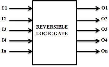
The reversible logic gate will generate unique output vector from unique input vector or vice-versa.In reversible logic, Input vector isIv=(I1,I2,I3…In ) and Output vector is Ov=( O1,O2,O3……On ), For each particular vector j Iv ↔ Ov.
Figure:1shows a general reversible gate; the gate will be having k inputs and k outputs and it is called ak*k reversible gate. In reversible gates, fan-out are not permitted. No feedback paths are allowed i.e. circuit is acyclic. Some important factors are Garbage output, constant input etc. Garbage output is the un-utilized output from the reversible gate, very much essential to achieve reversibility and it must be not used for further computation. Constant inputs are those that will be added to k*k function to make it reversible. For an optimized reversible circuit, the number of garbage outputs, the number of constant inputs and the number of reversible gates used should be minimum.
Fig 1:general reversible gate
In the design of reversible logic circuits the following points must be considered to achieve an optimized circuit. They are:
Fan-out is not allowed.
Loop or feedback is not permitted. Garbage outputs should be minimum. Minimum delay.
Minimum quantum cost.
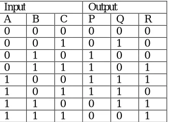
FREDKIN GATE (FRG) :
The input vector is I(A, B, C) and the output vector is O(P, Q, R). The output is defined by P=A, Q=A'B ^ AC and R=A'C ^ AB. The Quantum cost of a Fredkin gate is 5.
ISSN(Online): 2319-8753 ISSN (Print) : 2347-6710
I
nternational
J
ournal of
I
nnovative
R
esearch in
S
cience,
E
ngineering and
T
echnology
(A High Impact Factor, Monthly, Peer Reviewed Journal)
Vol. 5, Issue 2, Februray 2016
TRUTH TABLE OF PARITY PRESERVING FREDKIN GATE:
Input Output
A B C P Q R
0 0 0 0 0 0
0 0 1 0 0 1
0 1 0 0 1 0
0 1 1 0 1 1
1 0 0 1 0 0
1 0 1 1 1 0
1 1 0 1 0 1
1 1 1 1 1 1
NEW FAULT TOLERANT GATE (NFT) :
The NFT gate is a 3*3 Reversible gate with three inputs and three outputs[8]. The input vector is I(A, B, C) and the output vector is O(P, Q, R). The output is defined by P=A^B, Q=BC^AC’, R=BC^AC'and is shown in the Fig. 4.The Quantum cost of a NFT gate is 5.
Fig 3: 3*3 NFT gate.
TRUTH TABLE OF PARITY PRESERVINGNFT GATE:
Input Output
A B C P Q R 0 0 0 0 0 0 0 0 1 0 1 0 0 1 0 1 0 0 0 1 1 1 0 1 1 0 0 1 1 1 1 0 1 1 1 0 1 1 0 0 1 1 1 1 1 0 0 1
MODIFIED IG GATE (MIG) :
ISSN(Online): 2319-8753 ISSN (Print) : 2347-6710
I
nternational
J
ournal of
I
nnovative
R
esearch in
S
cience,
E
ngineering and
T
echnology
(A High Impact Factor, Monthly, Peer Reviewed Journal)
Vol. 5, Issue 2, Februray 2016
Fig 4: 4*4 MIG gate.
TRUTH TABLE OF PARITY PRESERVING MIG GATE
Input Output
A B C D P Q R S 0 0 0 0 0 0 0 0 0 0 0 1 0 0 0 1 0 0 1 0 0 0 1 0 0 0 1 1 0 0 1 1 0 1 0 0 0 1 0 0 0 1 0 1 0 1 0 1 0 1 1 0 0 1 1 0 0 1 1 1 0 1 1 1 1 0 0 0 1 1 0 1 1 0 0 1 1 1 0 0 1 0 1 0 1 1 1 1 1 0 1 1 1 1 1 0 1 1 0 0 1 0 1 0 1 1 0 1 1 0 1 1 1 1 1 0 1 0 0 0 1 1 1 1 1 0 0 1
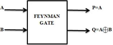
FEYNMAN GATE
Feynman gate is a 2x2 reversible gate. The input vector is I(A,B) and the output vector is O(P,Q).The output defined by P=A,Q=A ^B. Quantum cost of a Feynman gate is 1.Feynman gate can be used as copying gate.
Fig 5: 2*2 Feynman gate
INPUT OUTPUT
A B C P Q R
0 0 0 0 0 0
0 0 1 0 0 1
0 1 0 0 1 0
0 1 1 0 1 1
1 0 0 1 0 0
1 0 1 1 0 1
1 1 0 1 1 1
ISSN(Online): 2319-8753 ISSN (Print) : 2347-6710
I
nternational
J
ournal of
I
nnovative
R
esearch in
S
cience,
E
ngineering and
T
echnology
(A High Impact Factor, Monthly, Peer Reviewed Journal)
Vol. 5, Issue 2, Februray 2016
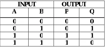
TRUTH TABLE OF FEYNMAN GATE
INPUT OUTPUT
A B P Q
0 0 0 0
0 1 0 1
1 0 1 1
1 1 1 0
TOFFOLI GATE:
Toffoli gate is 3x3 reversible gate. The input vector is I(A,B,C) and the output vector is O(P,Q,R).The outputs are defined by P=A,Q=B,R=ABC. Quantum cost of a TOFFOLI gate is 5.
fig 6: 3*3 Toffoli gate TRUTH TABLE OF TOFFOLI GATE:
PERES GATE:
Peres gate is 3x3 reversible gate. The input vector is I(A,B,C) and the output vector is O(P,R,S).The output is defined by P=A,Q=A+ B and R=ABC. Quantum cost of a Peres gate is 4.
Fig 7: Peres gate TRUTH TABLE OF PERES GATE:
INPUT OUTPUT
A B C P Q R
0 0 0 0 0 0
0 0 1 0 0 1
0 1 0 0 1 0
0 1 1 0 1 1
1 0 0 1 1 0
1 0 1 1 1 1
1 1 0 1 0 1
ISSN(Online): 2319-8753 ISSN (Print) : 2347-6710
I
nternational
J
ournal of
I
nnovative
R
esearch in
S
cience,
E
ngineering and
T
echnology
(A High Impact Factor, Monthly, Peer Reviewed Journal)
Vol. 5, Issue 2, Februray 2016
DOUBLE PERES GATE (DPG)
DPG gate is 4x4 reversible gate. The input vector is I(A,B,C,D) and the output vector is O(P,Q,R,S). The output is P=A,Q=A⊕B,R=A⊕B⊕D and S=(A⊕B)D⊕AB⊕C. Quantum cost of DPG gate is 6.It can work singly as Reversible full adder with C=0 and D=Cin.
fig 8: 4*4 dual peres gate
TRUTH TABLE OF DUAL PERES GATE:
INPUT OUTPUT
A B C D P Q R S
0 0 0 0 0 0 0 0
0 0 0 1 0 0 0 1
0 0 1 0 0 0 1 0
0 0 1 1 0 0 1 1
0 1 0 0 0 1 1 0
0 1 0 1 0 1 1 1
0 1 1 0 0 1 0 1
0 1 1 1 0 1 0 0
1 0 0 0 1 1 1 0
1 0 0 1 1 1 1 1
1 0 1 0 1 1 0 1
1 0 1 1 1 1 0 0
1 1 0 0 1 0 0 1
1 1 0 1 1 0 0 0
1 1 1 0 1 0 1 1
1 1 1 1 1 0 1 0
CARRY LOOK-AHEAD ADDER
Carry look-ahead adder are fastest adder of all adders because it calculates the carry bits before the summation. Carry look-ahead adder actually determines the carry bit by two modules first is “generate a carry” and second is “propagate a carry”. Carry signal will be generated in two conditions. When both bits Ai and Bi are equal to 1 or when carry-in is 1 and Ai or Bi is 1.
Carry propagation (Pi) and Carry generation (Gi) are Pi = Ai ⊕ Bi
Gi = Ai Bi
Sum signal can be calculated as follows:
ISSN(Online): 2319-8753 ISSN (Print) : 2347-6710
I
nternational
J
ournal of
I
nnovative
R
esearch in
S
cience,
E
ngineering and
T
echnology
(A High Impact Factor, Monthly, Peer Reviewed Journal)
Vol. 5, Issue 2, Februray 2016
Carry signal can be calculated as Ci+1 = Gi ⊕ Pi Ci
Applying this to a 4-bit adder ,we have: C1 = G0 ⊕ P0C0
C2 = G1 ⊕ P1C1 = G1 ⊕ P1(G0 ⊕ P0C0) C3 = G2 ⊕ P2C2 = G2 ⊕ P2(G1 ⊕ P1C1)
Partial Full Adder (PFA): This adder generates Gi, Pi and Si. Pi = Ai⊕Bi,
Gi= Ai.Bi, Si= Ai⊕Bi⊕Ci
Fig 9: Partial full adder
REVERSIBLE LOGIC CARRY LOOK AHEAD ADDER:
ISSN(Online): 2319-8753 ISSN (Print) : 2347-6710
I
nternational
J
ournal of
I
nnovative
R
esearch in
S
cience,
E
ngineering and
T
echnology
(A High Impact Factor, Monthly, Peer Reviewed Journal)
Vol. 5, Issue 2, Februray 2016
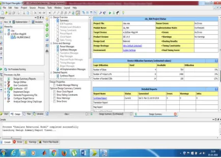
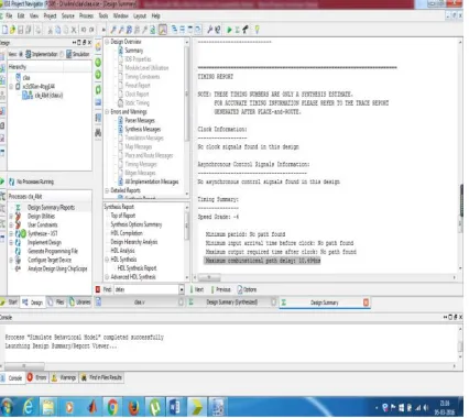
III. RESULT
SIMULATION OUTPUT:
Fig 11:simulation output
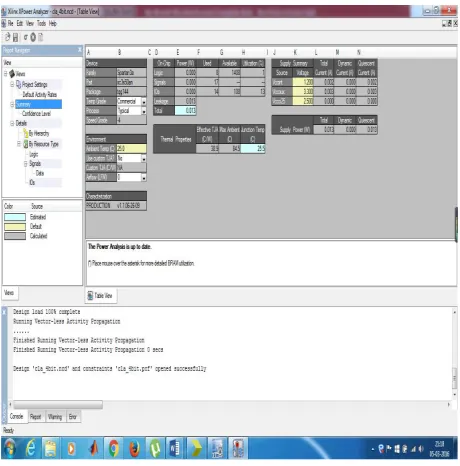
AREA:
ISSN(Online): 2319-8753 ISSN (Print) : 2347-6710
I
nternational
J
ournal of
I
nnovative
R
esearch in
S
cience,
E
ngineering and
T
echnology
(A High Impact Factor, Monthly, Peer Reviewed Journal)
Vol. 5, Issue 2, Februray 2016
CALCULATE DELAY:
Fig 13: performance of delay
RTL DIAGRAM
ISSN(Online): 2319-8753 ISSN (Print) : 2347-6710
I
nternational
J
ournal of
I
nnovative
R
esearch in
S
cience,
E
ngineering and
T
echnology
(A High Impact Factor, Monthly, Peer Reviewed Journal)
Vol. 5, Issue 2, Februray 2016
PROCESS OF TECHNOLOGY:
Fig 15: Technology diagram
ISSN(Online): 2319-8753 ISSN (Print) : 2347-6710
I
nternational
J
ournal of
I
nnovative
R
esearch in
S
cience,
E
ngineering and
T
echnology
(A High Impact Factor, Monthly, Peer Reviewed Journal)
Vol. 5, Issue 2, Februray 2016
IV. CONCLUSION
Reversible logic gates are used to Reduced the power consumption, Minimum delay ,Garbage outputs should be minimum, Minimum quantum cost, performance is high due to area is reduced.
REFERENCES
[1] Ashima Malhotra, Charanjit Singh, Amandeep Singh, “Efficient Design of Reversible Multiplexers with Low Quantum Cost and Power Consumption’’, International Journal of Emerging Technology and Advanced Engineering, Volume 4, Issue 7, July 2014.
[2] Ashima Malhotra, Charanjit Singh, Amandeep Singh, “Efficient Design of Reversible Multiplexers with Low Quantum Cost’’, International Journal of Engineering Research and Applications, Volume 4, Issue 7, July 2014.
[3] B.Raghu Kanth, “A Distinguish between reversible and conventional logic gates”, International Journal of Engineering Research and Application, Vol. No.2, Issue No.2,pp.148-151,2012.
[4] Lafifa Jamal, Md.Shamsujjoha,Hafiz Md.Hasan Babu, “Design of Optimal Reversible Carry Look-ahead Adder with Optimal Garbage and Quantum Cost”, International Journal of Engineering and Technology,Vol.No.2, 2012.
[5] Prashant.R.Yelekar, “Introduction to reversible logic gates and its application”, 2nd National Conference on Information and communication
Technology, 2011.
[6] Y. Cao, Predictive Technology Model for Robust Nanoelectronic Design. New York, NY, USA: Springer-Verlag, 2011. [7] D.Michael Miller and Zahra Sasanian, “Lowering the quantum gate cost of reversible circuits”, IEEE, 2010.
[8] J. Kwong, Y. K. Ramadass, N. Verma, and A. P. Chandrakasan,“A 65 nm sub-Vt microcontroller with integrated SRAM and switched capacitor DC-DC converter,” IEEE J. Solid-State Circuits, vol. 44, no. 1, pp. 115–126, Jan. 2009.