Study of low dimensional SiGe island on Si for potential visible
Metal-Semiconductor-Metal photodetector
Alhan Farhanah Abd Rahim1, *, Nur’Amirah Zainal Badri1 , Rosfariza Radzali1 and Ainorkhilah Mahmood2
1Faculty of Electrical Engineering, Universiti Teknologi MARA Cawangan Pulau Pinang,13500 Permatang Pauh, Penang, Malaysia 2Department of Applied Sciences, Universiti Teknologi MARA Cawangan Pulau Pinang,13500 Permatang Pauh, Penang, Malaysia
Abstract. In this paper, an investigation of design and simulation of silicon germanium (SiGe) islands on silicon (Si) was presented for potential visible metal semiconductor metal (MSM) photodetector. The characterization of the performances in term of the structural, optical and electrical properties of the structures was analyzed from the simulation results. The project involves simulation using SILVACO Technology Computer Aided Design (TCAD) tools. The different structures of the silicon germanium (SiGe) island on silicon substrate were created, which were large SiGe, small SiGe, combination SiGe and bulk Ge. All the structures were tested for potential Metal Semiconductor Metal (MSM) photodetector. The extracted data such as current versus voltage characteristic, current gain and spectral response were obtained using ATLAS SILVACO tools. The performance of SiGe island structures and bulk Ge on Si substrate as (MSM) photodetector was evaluated by photo and dark current-voltage (I-V) characteristics. It was found that SiGe islands exhibited higher energy band gap compared to bulk Ge. The SiGe islands current-voltage characteristics showed improved current gain compared to bulk Ge. Specifically the enhancement of the islands gain was contributed by the enhanced photo currents and lower dark currents. The spectral responses of the SiGe islands showed peak response at 590 nm (yellow) which is at the visible wavelength. This shows the feasibility of the SiGe islands to be utilized for visible photodetections.
1 Introduction
Recent integrated circuit (IC) technology used millions of transistors on a small of silicon die [1]. Silicon is most commonly used semiconductor for the technology [2]. Low dimensional structures can be defined as structures and components that will improve physical, chemical, and biological properties that result in new phenomena and processes due to their nanoscale size [3]. Hence making SiGe into small sizes are expected to tailor the energy band gap of the SiGe [4].
At the complementary metal oxide semiconductor (CMOS) and bipolar CMOS (BiCMOS) technologies, silicon germanium is an important material for the fabrication of SiGe heterojunction bipolar transistors and strained Si metal oxide semiconductor (MOS) transistors [5]. Besides, the combination between the silicon germanium and the silicon will produce a heterojunction that also a benefit to silicon homojuction [6]. Silicon Germanium quantum dots have a way to reach high performance hybrid photonics circuitry within CMOS platforms [7]. For the improved light emission properties at telecommunication wavelengths with higher activation energies and improved ratio of radiative to non-radiative recombination, it used the self-assembled of germanium islands on silicon [8]. Si and SiGe is indirect semiconductor which unable to emit and detect light at visible spectrum [9]. Germanium has very favourable
properties as a semiconductor, when compared to silicon whereby germanium has a much higher mobility of electrons and holes than silicon [10].
2
Methodology
2.1. Silvaco Technology Computer Aided (TCAD)
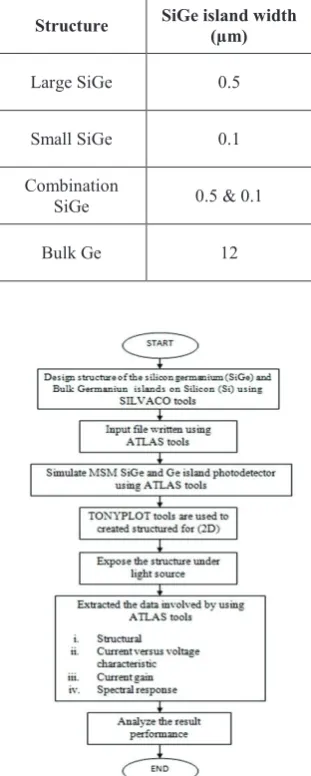
The project started with design and simulation of SiGe islands on Si using SILVACO tools. The project involved the construction of the four different structures of SiGe islands on silicon substrate. The four SiGe structures were varied in term of their island diameters. Table 1 shows the structures which are large SiGe, small SiGe, combination SiGe and bulk Ge. Fig. 1 shows the flowchart of the steps undertaken for the project that involved the simulation of the structures.
Table 1. Size of SiGe islands and Bulk Ge on Si substrate.
Structure SiGe island width (µm)
Large SiGe 0.5
Small SiGe 0.1
Combination
SiGe 0.5 & 0.1
Bulk Ge 12
Fig. 1. Flowchart for simulation of SiGe islands on Si using ATLAS Silvaco TCAD tools.
In ATLAS, each file must contain five groups of statements in the correct order [12]. Failure to follow the order will usually cause termination of the program and an error message, then lead to incorrect operation of the program [13]. Table 2 shows ATLAS command group
that involved in the simulation of the structures to characterize the device performance.
Table 2. ATLAS commands with the primary statements [13].
Group Statements
Structure
Specification Electrode, Doping Mesh, Region,
Material Model
Specification Material, Models, Contact, Interface
Numerical Method
Selection Method
Solution
Specification Log ,Solve, Load, Save
Result analysis Extract, Tonyplot
The process simulation started with the first part where the structures were constructed and simulated for four different island sizes using ATLAS tools. In the ATLAS input file, the Si substrate was first initialized, and the mesh was defined by setting the x- and y-mesh. Fig. 2 shows the fine mesh defined at the islands region and the wetting layer regions (underneath the island) whereas coarse mesh were tabulated around the substrate.
Fig. 2. Mesh defination for large structure of islands.
The construction of the SiGe islands MSM photodetector is the second part in the simulation of the project. During the second part, the region and contact statements were set. The example coding written for the islands are shown in Table 3.
The fine mesh of the structure
SiGe islands Air gap
Table 3. Region and contact specification for MSM photodetector for large structure of islands in ATLAS.
ATLAS input file coding
Defining region and materials
region num=4 x.min=0.5
x.max=1.0 y.min=0.05 y.max=0.25 material=SiGe
Defining contact (anode &
cathode)
electr name=anode x.min=2.0 x.max=2.5 y.min=0.05 y.max=0.25 electr name=cathode x.min=9.5 x.max=12.0 y.min=0.0 y.max=0.1
The next step of the simulation is setting up the material and physical model in the input file. In Silvaco TCAD tools, there are wide number of physical model such as models for recombination, photogeneration, mobility and lifetime [14]. The project used AUGER recombination model for the physical model as shown in Table 4. Precise selection for type of physical model is really important for accurate simulation process [13].
Table 4. Physical model coding
Type of
physical model Physical model coding in ATLAS input file
AUGER MODEL
physical models
model conmob fldmob srh auger print
Then, to check the photo response of the photodetector, the light source was exposed to the sample by defining the beam power and its respective wavelength. Table 5 shows the solution specification for the biasing of the device and the setting of the light source that had been applied to the SiGe islands on Si MSM photodetector. The photodetector was biased from 0.5 V to 5 V. Fig. 3 shows the light source (power beam) shined onto the large island of the SiGe structure. Nickel (Ni) contact has been used by defining the work function of 5.01 eV. The Ni contact was chosen in order to obtain Schottky behaviour for the photodetector.
Table 5. Solution specification and beam power setting
ATLAS input file
Solution specification
and beam power coding
method newton trap solve init
log outfile=I-Vpho.log
solve b1=750 vanode=0.5 vstep=0.1 vfinal=5.0 name=anode
Tonyplot I-Vdark.log -overlay I-Vpho.log -I-Vpho.set
Fig. 3. Light source applied to the structure.
Lastly, the current-voltage (I-V) characteristic was obtained from the simulation, then the performance of photodetection was being evaluated by extracting the current gain which is the ratio of the photo current (Ip) over the dark current (Id). The energy band gap (Eg) and spectral response of the photodetector were also being characterized.
3 Result and discussion
3.1 Structural characteristics of the SiGe islands
The structure of different islands was created from the simulation. Fig. 4 shows the notation of the region and material in the structures.
Fig. 4. Label identification of the region and material of the structure.
Fig. 5 shows the structure of the large SiGe, small SiGe and combination SiGe islands. The bulk Ge also included to compare the characteristic of the properties with the islands. The dark green colour represents SiGe islands and Ge bulk.
(a) Light Source
Large SiGe
Anode
Cathode
Air
(b)
(c)
(d)
Fig. 5. Final structures for (a) large SiGe (0.5µm width), (b) small SiGe (0.1µm width), (c) combination SiGe (0.5µm – 0.1µm width) islands on Si substrate and (d) bulk Ge (12 µm width on Si substrate.
3.2 Bandgap of the structure
The band gap for the SiGe islands and the bulk Ge were extracted from the simulation as shown in Fig. 6. It can be seen that altering the island sizes has no cause to the changes in the band gap of the SiGe structures. However, alloying Si to Ge which is SiGe (Eg = 1.5 eV) does increase the band gap compared to Ge bulk (Eg = 0.8 eV). This agrees with the quantum confinement effect which stated that decreasing crystallite size will increase the band gap [15]. In addition, the increase in the bandgap indicate the potential for visible photodetection by the SiGe island on Si substrate whereby a change from indirect semiconductor to direct semiconductor will lead to the enhance photon absorption.
(a)
(b)
Fig. 6. Extracted bandgap of (a) SiGe islands and (b) bulk Ge.
3.3 I-V Characteristic and Gain (Ip/Id) of the structures
The metal finger contact was deposited on the SiGe islands and also bulk Ge to form metal-SiGe islands-metal photodetector and to analyse the potential of the structures for optoelectronic application. Fig. 7 presents the three SiGe island samples, then bulk Ge was included as the control sample to compare for the current-voltage (I-V) characteristics of the MSM photodetectors measured under the illumination of light (Ip) and under dark (Id). The current of the SiGe islands MSM photodetector increases with the bias voltage and saturated gradually as the voltage reach 1V. It can be seen that SiGe islands for all different sizes produced lower dark current compared to bulk Ge. In addition, the SiGe island devices also produced higher photocurrents compared to the bulk Ge photodetector. This showed that upon photons illumination, all the different size of the SiGe islands exhibited tremendous responses, producing significant free carriers for the enhanced current conduction than the bulk Ge.
Eg=1.5eV
Eg=0.8eV
Bulk Ge
Si sub
Anode
Cathode
Air Combination
SiGe Small SiGe
Anode
Cathode
Cathode
Anode
Air
Fig. 7. I-V characteristic SiGe islands and bulk Ge.
Fig. 8 shows current gain for the SiGe islands and bulk Ge, to analyze the performance for photodetection. The current gain is the ratio of photo current-to-dark current. The result of the current gain shows that the three SiGe islands obtained higher current gain compared to bulk Ge. The higher photo currents from the SiGe islands were attributed to the optical phonon confinement of the low dimensional SiGe and the higher SiGe mobility than the bulk Ge.
Fig. 8. Current gain of the three SiGe islands and bulk Ge.
3.4 Spectral Response
Fig. 9 shows the spectral response of the SiGe islands and bulk Ge from deep UV to infrared regions. Interestingly, all the SiGe islands devices exhibited significant response towards yellow regions (visible light). Specifically, the three SiGe islands devices showed peak current at the same wavelength of 0.59 µm, while bulk Ge at 0.94µm respectively. Therefore, the SiGe Island on Si devices show potential for photodetection at visible (yellow) spectrum, while the bulk Ge shows no response over the visible spectrum.
Fig. 9. Spectral response of SiGe islands and bulk Ge.
3.5 Schottky Barrier Height
Schottky barrier height which will probe the quality of the Schottky contacts was extracted to further analyze the performance of the MSM photodetector. The quality of the interface between the deposited metal (Ni) and the semiconductor surface (SiGe islands and Ge bulk) and the nature of the current transport across this interface has been extracted to determine the performance and reliability of the Schottky contacts. The thermionic emission theory is the model used to study the forward I-V characteristics of a Schottky diode [8]. According to this theory, the diode current, Id is described by the following equation [8],
Id = Ioexp(qVd / nkT) [1-exp(-qVd / kT)] (1)
where Vd is the voltage across the diode, n is the ideality factor (which may depend on temperature and independent on voltage), k is the Boltzman constant, and Io is the saturation current given by:
Io = AA**T2exp [-qφB / k] (2)
where q is the electron charge, T is the temperature, A is the contact area, A** is the effective Richardson constant and φB is the Schottky barrier height [8]. The
saturation current, Io is mainly determined by the barrier height φB and the effective Richardson constant A** [8].
Equation (1) at V>3kT/q, can be simplified to:
Id = Io exp( qVd / nkT) (3)
The theoretical value of A** can be calculated using A** = 4πm*qk2/h3. The plot of ln Id versus Vd will give a straight line with a slope of q/(nkT), and the intercept with y-axis will yield I0 in which Schottky barrier height, φB can be obtained using Io = AA**T2exp [-qφB / k] (2).
The Schottky barrier height for dark current of SiGe islands and bulk Ge on Si substrate were listed as shown in Table 6. It was observed that the SiGe islands exhibited lower dark currents compared to bulk Ge. This in agreement with the larger schottky barrier height (SBH) of the SiGe islands compared to bulk Ge. The lowest dark current of the SiGe islands could be attributed to the high barrier height of the metal contact
max = 0.59µm
than the bulk Ge that have higher of dark current. In addition, the lower dark currents of the SiGe islands also contributed to the higher resistance for the devices.
Table 6. Data extracted from (I-V) characteristics graph for dark current situation.
Large
SiGe Small SiGe Combination SiGe Bulk Ge SBH
in dark
(eV)
0.931 0.937 0.948 0.845
Id at 5V
(A) 7.01E-10 4.24E-10 3.55E-10 2.32E-04
Ip at 5V
(A) 3.30E-07 4.06E-07 4.67E-07 6.31E-04
Rs
(Ω) 7.E+10 1.E+10 1.E+10 2.16E+04
Gain
at 5V 470.76 957.55 1315.49 2.73
4 Conclusion
As a conclusion, the structure of the silicon germanium (SiGe) islands and bulk Germanium (Ge) on Silicon (Si) have been successfully designed and simulated for potential visible metal semiconductor metal (MSM) photodetector using SILVACO TCAD tools. It is shown that the SiGe islands exhibited higher energy band gap (1.5eV) compared to bulk Ge (0.8eV). It is believed that the quantum confinement effect of the low dimensional SiGe island structure is responsible for the enhanced photo response and lower dark current. The SiGe islands produced higher photocurrents and lower dark currents compared to the bulk Ge. Moreover, SiGe Island on Si devices exhibited photoresponse at 0.59 µm of visible (yellow) spectrum but bulk Ge at 0.94 µm which is at infrared (red) spectrum region. Hence, the SiGe islands on the Si substrate provide better performance than Ge bulk for the potential visible metal semiconductor metal (MSM) photodetector.
The author wishes to thank Universiti Teknologi MARA for financial assistance and members of the IC Design Laboratory, and Department of Applied Science, Universiti Teknologi Mara Pulau Pinang, for endless technical assistance. Support from the Fundamental Research Grant Scheme (600-IRMI/FRGS 5/3(0107/2016) is gratefully acknowledged.
References
1. Y. An, A. Behnam, E Pop, and A.Ural. Appl. Phys. Lett. 102, 013110 (2013).
2. S. Bhushan, S. Sarangi, G. K. S, and A. Santra. J. of Semicond. Tech. and Sc. 13(4), 367-380 (2013). 3. N. U. R. Ershadiah, B. Abdul. Thesis /
Undegraduate Project Paper, Falculty of Electrical Engineering, Universiti Teknologi Malaysia(2011).
4. L. Nataraj. D.Eng., University of Delaware, 183, 3440493 (2010)
5. M. A. A. Hamid and F.Sulaiman. Int. J. of Elec. and Electronic Sys. Res 5, 67-73 (2012).
6. D. V. Shenai, , R. L. DiCarlo Jr, M. B. Power, A. Amamchyan, R. J. Goyette and E. Woelk. Journal of Crystal Growth 298, 172–175(2007).
7. V. V. Chandroday, N. Tiwari, J. S. Parmar, and G. S. Mittal. Int. J. of Eng. and Tech. Res. (IJETR) 2, 187-190 (2014)
8. P. Behera and S. K. Mohapatra. Int. J. of Adv. Sci. and Tech. 71, 59-66 (2014)
9. A. Baharin and M. R. Hashim. Semicond. Sci. Technol. 22, 905–910 (2007)
10. M. A. Bilya and M. H. Sani. International Journal of Science and Research (IJSR) 5 (2), 1137-1140 (2016)
11. H. Batwani, M. Gaur, and M. J. Kumar. The Int. J. for Comp. and Math. in Elec. and Electronic Eng. 28, 353–371 (2009).
12. M. Kaifi, M. J. Siddiqui, T. A. Abbasi, and M. U. Khan. J. of Electronic and Electrical Eng., 1, 9-12 (2010).
13. D. S. Software. ATLAS User’ s Manual, 567–1000 (2006)
14. V. Subramanian, S. Member, and K. C. Saraswat. IEEE Trans. on Electron Dev. 45, 1690-1695 (1998).