Western University Western University
Scholarship@Western
Scholarship@Western
Electronic Thesis and Dissertation Repository
1-23-2019 10:30 AM
Bouncing Dynamics of a Class of MEM/NEM Switching Systems
Bouncing Dynamics of a Class of MEM/NEM Switching Systems
Mohamed Bognash
The University of Western Ontario
Supervisor
Dr. S. F. Asokanthan
The University of Western Ontario
Graduate Program in Mechanical and Materials Engineering
A thesis submitted in partial fulfillment of the requirements for the degree in Doctor of Philosophy
© Mohamed Bognash 2019
Follow this and additional works at: https://ir.lib.uwo.ca/etd
Part of the Acoustics, Dynamics, and Controls Commons, Dynamics and Dynamical Systems
Commons, Electro-Mechanical Systems Commons, and the Other Engineering Science and Materials
Commons
Recommended Citation Recommended Citation
Bognash, Mohamed, "Bouncing Dynamics of a Class of MEM/NEM Switching Systems" (2019). Electronic Thesis and Dissertation Repository. 5997.
https://ir.lib.uwo.ca/etd/5997
This Dissertation/Thesis is brought to you for free and open access by Scholarship@Western. It has been accepted for inclusion in Electronic Thesis and Dissertation Repository by an authorized administrator of
ABSTRACT
The aim of the present research is to understand the bouncing dynamic behavior of NEM/MEM switches in order to improve the switch performance and reliability. It is well known that the bouncing can dramatically degrade the switch performance and life; hence, in the present study, bouncing dynamics of a cantilever-based NME/MEM switch has been studied in detail. To this end, a model of a MEM switch that incorporates electrostatic force, squeeze film air damping force as well as asperity-based contact force has been proposed for an electrostatically actuated switch. An actuation force due to piezoelectric effects is further included in an alternative micro-switch model of combined actuation for the purposes of bounce mitigation. For a NEM switch, an asperity-based contact model along with repulsive van der Waals force are incorporated in a nano-switch to capture the contact dynamics. Intermolecular forces, surface effects, and gas rarefication effects are also included in the NEM switch model. Further, an intermolecular force, specifically the Casimir force, is also used to actuate this class of switches in addition to the classical electrostatic actuation. Euler-Bernoulli beam theory and an approximate approach based on Galerkin’s method have been employed for predicting transient dynamic responses. In the present study, performance parameters such as initial contact time, permanent contact time, major bounce height, and the number of bounces have been quantified in the presence of interactive system nonlinearities.
ii
For a NEM switch, the performance parameters are also used to investigate the influence of surface effects and rarefication effects on the performance of an electrostatically actuated switch. Influence of some pull-in parameters on the switch bouncing behavior have also been investigated in the presence of surface effects at different vacuum conditions for purely Casimir actuated NEM switch. Recommended operating conditions or actuation parameters are suggested for the purposes of avoiding excessive bouncing for both types of NEM switches.
The present investigation on the bouncing dynamic behavior of a class of MEM/NEM switches is envisaged to yield greater insight into the design, reliability and performance predictions for this class of switches.
CO-AUTHORSHIP
iv
ACKNOWLEDGEMENTS
I would like to express my gratitude to those who provided me with encouragement and assistance during this thesis work.
I am deeply indebted to my thesis supervisor Dr. S. F. Asokanthan for introducing me to this research area and for his continuous guidance, encouragement and expertise and valuable contribution to this thesis. It simply would not have been possible without him.
My thanks also go to my colleagues and friends for their help and friendliness. It is very fortunate for me to work in such a good company.
TABLE OF CONTENTS Page
ABSTRACT i
CO-AUTHORSHIP ii
ACKNOWLEDGEMENTS iv
TABLE OF CONTENTS v
LIST OF TABLES vi
LIST OF FIGURES ix
NOMENCLATURE x
CHAPTER 1 INTRODUCTION AND LITERATURE REVIEW
1.1 Introduction 1
1.1.1 Introduction to MEM switches 4
1.1.2 Introduction to NEM switches 5
1.2 Literature review 6
1.2.1 MEM switches 7
1.2.2 NEM switches 12
1.3 Research objectives 17
1.4 Thesis outline 19
CHAPTER 2 MODELING OF A MEM SWITCH
2.1 Introduction 21
2.1 Equations of motion for a switch under electrostatic actuation 21
2.1.1 Electrostatic force 23
2.1.2 Squeeze-film damping force 23
2.1.3 Contact force 25
2.2 Equations of motion for a switch under combined electrostatic and
piezoelectric actuation 27
vi
2.4 Discretized model for response predictions 31
2.5 Response predictions 33
2.6 Conclusions 34
CHAPTER 3 BOUNCING DYNAMIC ANALYSIS AND MITIGATION FOR A MEM SWITCH
3.1 Introduction 35
3.2 Switch response under electrostatic actuation 35
3.3 Switch performance under harmonic dither in actuation voltage 42
3.4 Switch performance under combined actuation of electrostatic step
voltage and harmonic dither in the secondary actuator voltage 52
3.5 Conclusions 64
CHAPTER 4 UNCERTAINTY QUANTIFICATION BASED ON MEM SWITCH TIP BOUNCING
4.1 Introduction 66
4.2 Uncertainty quantification analysis 67
4.3 Conclusions 80
CHAPTER 5 MODELING OF A NEM SWITCH
5.1 Introduction 81
5.2 Intermolecular forces 82
5.2.1 Casimir force 83
5.2.2 Van der Waals force 84
5.3 Force due to surface effects and equivalent bending elasticity 86
5.4 Damping force 89
5.5 Equations of motion for a switch under electrostatic/pure Casimir
5.6 Conclusions 93
CHAPTER 6 BOUNCING DYNAMICS OF NEM SWITCHES UNDER ELECTROSTATIC AND PURE CASIMIR ACTUATION
6.1 Introduction 95
6.2 NEM switch under electrostatic actuation 96
6.3 NEM switch under pure Casimir actuation 105
6.4 Conclusions 114
CHAPTER 7 CONCLUSIONS AND RECOMMENDATIONS
7.1 Summary of results 116
7.2 Thesis contributions 119
7.3 Suggestions for future research 121
REFERENCES 122
viii
LIST OF TABLES Page
Table 3.1 MEM switch parameters and properties 36
Table 3.2 Predicted natural frequencies of the MEM switch 38
Table 3.3 PZT actuator parameters and properties 53
Table 3.4 Predicted natural frequencies of the MEM switch with PZT
layer 54
Table 4.1 MEM switch parameters and properties 68
LIST OF FIGURES Page
Fig. 1.1 Analog device inline MEMS series switch. 4
Fig. 1.2 NEM electrostatic switch with 30𝑛𝑚-thick beam and
20𝑛𝑚-thick air-gap. 6
Fig. 2.1 Typical cantilever beam type micro-switch with electrostatic
electrode. 22
Fig. 2.2 Contacting rough surfaces. 26
Fig. 2.3 Cantilever beam type micro-switch with electrostatic and
piezoelectric actuators. 28
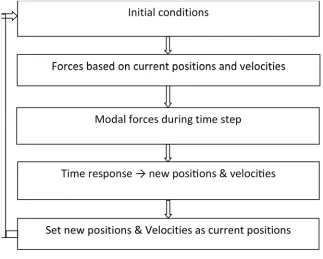
Fig. 2.4 Response prediction process. 33
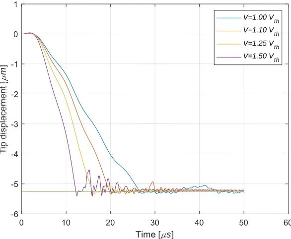
Fig. 3.1 Tip displacements for different actuation voltages. 37
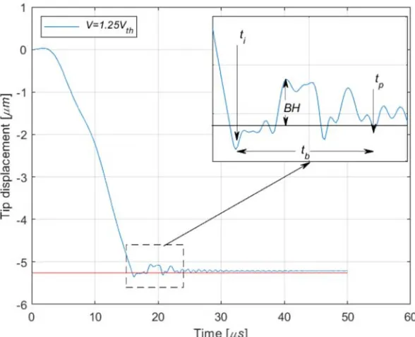
Fig. 3.2 Typical switch tip-end response for 𝑉 1.25 𝑉 . 39
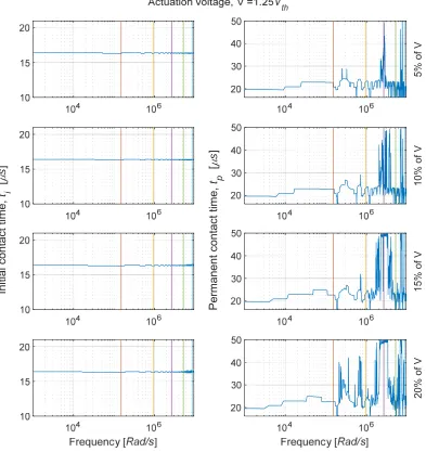
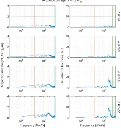
Fig. 3.3 Variation of initial contact time, permanent contact time,
and the bounce time vs. actuation voltages. 40
Fig. 3.4 Variation of major bounce height and number of bounces
vs. actuation voltages. 41
Fig. 3.5 (a)
Influence of frequency and amplitude of harmonic dither in electrostatic voltage on initial contact time and permanent
contact time for𝑉 1.1 𝑉 .
44
Fig. 3.5 (b)
Influence of frequency and amplitude of harmonic dither in electrostatic voltage on major bounce height and number of
bounces for 𝑉 1.1 𝑉 .
45
Fig. 3.6
Responses of step voltage and step voltage with harmonic
dither of 15% amplitude, 180543𝑟𝑎𝑑/𝑠 frequency at 𝑉
1.1 𝑉 .
46
Fig. 3.7 (a)
Influence of frequency and amplitude of harmonic dither in electrostatic voltage on initial contact time and permanent
contact time for𝑉 1.25 𝑉 .
x Fig. 3.7 (b)
Influence of frequency and amplitude of harmonic dither in electrostatic voltage on major bounce height and number of
bounces for 𝑉 1.25 𝑉 .
48
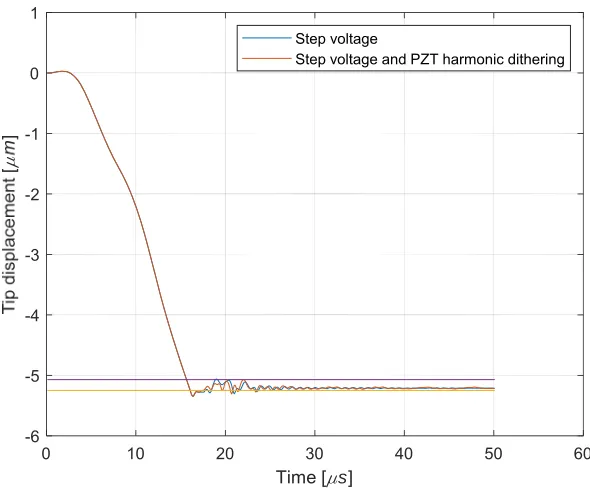
Fig. 3.8
Response of step voltage and step voltage with of harmonic
dither of 15% amplitude, 180543 𝑟𝑎𝑑/𝑠 frequency at 𝑉
1.25 𝑉 .
49
Fig. 3.9 (a)
Influence of frequency and amplitude of harmonic dither in electrostatic voltage on initial contact time and permanent
contact time for𝑉 1.5 𝑉 .
50
Fig. 3.9 (b)
Influence of frequency and amplitude of harmonic dither in electrostatic voltage on major bounce height and number of
bounces for 𝑉 1.5 𝑉 .
51
Fig. 3.10
Responses of step voltage and step voltage with of harmonic
dither of 20% amplitude, 380386 𝑟𝑎𝑑/𝑠 frequency at 𝑉
1.5 𝑉 .
52
Fig. 3.11 (a)
Influence of frequency and amplitude of harmonic dither in the PZT voltage on initial contact time and permanent contact
time for 𝑉 1.1 𝑉 .
56
Fig. 3.11 (b)
Influence of frequency and amplitude of harmonic dither in PZT voltage on major bounce height and number of
bounces for 𝑉 1.1 𝑉 .
57
Fig. 3.12
Responses of step voltage and step with harmonic dither in
PZT harmonic voltage of 10% amplitude, 647465 𝑟𝑎𝑑/𝑠
frequency at 𝑉 1.1 𝑉 .
58
Fig. 3.13 (a)
Influence of frequency and amplitude of harmonic dither in the PZT voltage on initial contact time and permanent
contact time for𝑉 1.25𝑉 .
59
Fig. 3.13 (b)
Influence of frequency and amplitude of harmonic dither in PZT voltage on major bounce height and number of
bounces for 𝑉 1.25 𝑉 .
Fig. 3.14
Responses of step voltage and step with harmonic dither in
PZT harmonic voltage of 15% amplitude, 1205005 𝑟𝑎𝑑/𝑠
frequency at 𝑉 1.25 𝑉 .
61
Fig. 3.15 (a)
Influence of frequency and amplitude of harmonic dither in the PZT voltage on initial contact time and permanent
contact time for𝑉 1.5 𝑉 .
62
Fig. 3.15 (b)
Influence of frequency and amplitude of harmonic dither in PZT voltage on major bounce height and number of
bounces for 𝑉 1.5𝑉 .
63
Fig. 3.16
Responses of step voltage and step with harmonic dither in
PZT harmonic voltage of 20% amplitude, 1681810 ra𝑑/𝑠
frequency at 𝑉 1.5 𝑉 .
64
Fig. 4.1 Typical switch tip-end response for 𝑉 1.25 𝑉 . 69
Fig. 4.2 (a) Uncertainties in asperity radius 𝑅 on or major bounce height
𝐵𝐻 for actuation voltages 1.25 𝑉 and 1.5 𝑉 . 70
Fig. 4.2 (b) Uncertainties in asperity radius 𝑅 on initial contact time 𝑡
for actuation voltages 1.25 𝑉 and1.5 𝑉 . 71
Fig. 4.3 (a)
Uncertainties in area density of asperities 𝜂 on major
bounce height 𝐵𝐻 for actuation voltages 1.25 𝑉
and 1.5 𝑉 .
72
Fig. 4.3 (b) Uncertainties in area density of asperities 𝜂 on initial
contact time 𝑡 for actuation voltages 1.25 𝑉 and1.5 𝑉 . 72
Fig. 4.4 (a) Uncertainties in in beam tip length 𝑙 on major bounce
height 𝐵𝐻 for actuation voltages 1.25 𝑉 and1.5 𝑉 . 73
Fig. 4.4 (b) Uncertainties in beam tip length 𝑙 on initial contact time 𝑡
for actuation voltages 1.25 𝑉 and 1.5 𝑉 . 74
Fig. 4.5 (a) Uncertainties in Young’s modulus 𝐸 on major bounce
height 𝐵𝐻 for actuation voltages 1.25 𝑉 and 1.5 𝑉 . 75
Fig. 4.5 (b) Uncertainties in Young’s modulus 𝐸 on initial contact time
xii
Fig. 4.6 (a) Uncertainties in beam width 𝑎 on major bounce height 𝐵𝐻
for actuation voltages 1.25 𝑉 and 1.5 𝑉 . 76
Fig. 4.6 (b) Uncertainties in beam width 𝑎 on initial contact time 𝑡 for
actuation voltages 1.25 𝑉 and 1.5 𝑉 . 77
Fig. 4.7 (a) Uncertainties in beam thickness 𝑏 on major bounce height
𝐵𝐻 for actuation voltages 1.25 𝑉 and 1.5 𝑉 . 77
Fig. 4.7 (b) Uncertainties in beam thickness 𝑏 on initial contact time 𝑡
for actuation voltages 1.25 𝑉 and 1.5 𝑉 . 78
Fig. 4.8 (a) Uncertainties in actuation voltage 𝑉 on major bounce
height 𝐵𝐻. 79
Fig. 4.8 (b) Uncertainties in actuation voltage 𝑉 on initial contact
time 𝑡. 79
Fig. 5.1 Schematic representation of active range for intermolecular
forces. 85
Fig. 5.2 Schematic of a bending NEM switch with surface effects. 87
Fig. 5.3 Typical cantilever beam type nano-switch with electrostatic
electrode. 91
Fig. 6.1 Typical time response of the switch tip. 98
Fig. 6.2 Damped oscillatory motion of nano switch under voltage
less than the dynamic pull-in voltage 99
Fig. 6.3 Influence of surface effects on initial contact time𝑡 at
various actuation voltages. 100
Fig. 6.4 Influence of surface effects on permanent contact time 𝑡 at
various actuation voltages and pressures. 101
Fig. 6.5 Influence of surface effects on bounce time 𝑡 at various
actuation voltages and pressures. 102
Fig. 6.6 Influence of surface effects on major bounce height 𝐵𝐻 at
various actuation voltages and pressures. 104
Fig. 6.7 Influence of surface effects on number of bounces 𝑁𝐵 at
Fig. 6.8 Static deflection of the Casimir actuated nano-beam. 106
Fig. 6.9 Typical Casimir actuated NEM switch tip-end response. 107
Fig. 6.10 Combination of lengths and gaps for Casimir actuation. 108
Fig. 6.11 Initial time contours𝑡 for length-gap combination of
Casimir actuated NEM switch. 109
Fig. 6.12 Permanent time contours 𝑡 for length-gap combination of
Casimir actuated NEM switch at various pressures. 110
Fig. 6.13 Bounce time contours 𝑡 for length-gap combination of
Casimir actuated NEM switch at various pressures. 111
Fig. 6.14 Major bounce height 𝐵𝐻for length-gap combination of
Casimir actuated NEM switch at various pressures. 112
Fig. 6.15 Number of major bounce 𝑁𝐵for length-gap combination of
xiv NOMENCLATURE
𝐴 beam’s cross-sectional area
𝑎 beam width
𝑎 piezoelectric layer width
𝐴 nominal contact area
𝐴 cross-sectional area of the piezoelectric layer
𝑏 beam thickness
𝑏 piezoelectric layer thickness
𝐵𝐻 major bounce height
𝐶 speed of light
𝐶 neutral axis of a section that includes the piezoelectric layer
𝐶 variable damping coefficient
𝑑 air gap
𝑑 piezoelectric constant
𝑑 beam tip contact gap
𝐸 Young’s modulus for the beam material
𝐸 Young’s modulus for the piezoelectric
𝐸 surface elastic modulus
𝐸𝐼 effective bending rigidity of the nano beam
𝑓 contact force per unit length of the beam
𝑓 Casimir force per unit length of the beam
𝑓 damping force per unit length of the beam
𝑓 electrostatic force per unit length of the beam
𝑓 distributed transverse load along the longitudinal direction of the beam due
to surface effects
𝑓 Van der Waals force per unit length of the beam
𝐴 Hamaker constant
𝐻 𝑥 Heaviside function
ℎ Planck’s constant divided by 2𝜋
𝐼 moment of inertia of the beam’s cross-section
𝑲 stiffness matrix
𝑘 gain
𝐾 Boltzmann’s constant
𝑘 stiffness matrix elements
𝐾 Knudsen number
𝐿 beam length
𝐿 , 𝐿 starting and ending points of electrostatic electrode
𝐿 , 𝐿 starting and ending points of piezoelectric secondary actuator
𝐿 beam tip length
𝑴 mass matrix
𝑚 mass matrix elements
𝑚 mass of the molecules
𝑀 distributed moment due to the piezoelectric actuator
𝑀 asperity height mean value
𝐵𝐻 major bounce height
𝑵 vector of modal forces
𝑁𝐵 number of single significant bounces
𝑛 number of modes
𝑛 unit normal vector to the surface
𝑃 pressure
𝑃 ambient atmospheric pressure
𝑃 applied load for contact
𝒒 vector of temporal coordinates
𝑞 𝑡 temporal coordinates
𝑅 radius of sphere asperity
𝑡 time
𝑡 initial contact time
xvi
𝑡 permanent contact time
𝑇 temperature
𝑉 actuation voltage
𝑉 piezoelectric actuation voltage
𝑉 theoretical pull-in dynamic voltage
𝑣 initial velocities
𝑤 contact interference
𝑥 spatial co-ordinate
𝑥 initial displacements
𝑌 𝑥 mode shapes
𝑧 cut-off value
𝑦 beam lateral deflection
𝛽 fringe effect correction coefficient
𝛿 𝑥 Dirac delta function
𝜀 equilibrium distance at which 𝑓 becomes zero
ε piezoelectric induced strain
ε longitudinal strain due to the piezoelectric
𝜖 longitudinal strain for nano beam
𝜀 permittivity of air
𝜂 area density of asperities
𝜅 beam curvature
𝜉 asperity height
λ mean free path of the molecule
𝜇 air viscosity
𝜌 material mass density of the beam (mass per unit volume)
𝜌 piezoelectric layer mass density
𝜎 , 𝜎 standard deviation in width, thickness
𝜎 standard deviation in Young’s modulus
𝜎 standard deviation in major bounce height𝐻
𝜎 standard deviation in beam tip length 𝐿
𝜎 standard deviation in radius of asperities
𝜎 standard deviation in initial contact time 𝑡
𝜎 standard deviation in actuation voltage𝑉
𝜎 standard deviation in area density of asperities
𝜎 , 𝜎 stresses above and below the surface interface, respectively
𝜏 surface stress
𝜏 residual surface stress
𝑣 , 𝑣 Poisson’s ratios of contact surfaces
1 CHAPTER 1
INTRODUCTION AND LITERATURE REVIEW
1.1 Introduction
Microelectromechanical Systems (MEMS) is an important area of technology that combines different engineering disciplines such as material, mechanical, electrical, chemical, optics and fluids. This technology integrates interrelated device components into comprehensive systems at very small scales that complete functions such as sensing and actuation (Ostasevicius & Dauksevicius, 2010). The characteristic length of MEM devices
is typically less than 1𝑚𝑚 but more than 1𝜇𝑚. With the new advancement in
nanofabrication methods, a size reduction of microelectromechanical systems originates the nanoelectromechanical systems (NEMS) in which the characteristic length of NEM
devices is less than 1𝜇𝑚. Advantages of MEMS/NEMS technology such as low-cost, low
power consumption, high functionality, and small size and light weight of the devices open enormous opportunities in the commercial markets and make them attractive for many engineering applications (Leondes, 2006, Voiculescu & Zaghloul, 2016).
Recent advances in MEMS/NEMS technology have led to development of a multitude of new devices that can be used in a variety of industrial as well as consumer product applications. The wide range of applications for MEMS/NEMS could be classified into four main categories: (1) sensors, gathering information from environments; (2) actuators, controlling the environment by positioning, regulating, pumping, and filtering in response to actuation sources; (3) switches, such as two-terminal and three-terminal relays; (4) resonators; such as oscillators and filters in communication systems and signal processing applications (Ma, 2011).
Among these applications, switches are fundamental building blocks in the design of MEMS/NEMS. These structures have advantages of low power consumption, low insertion loss, and high isolation. MEM/NEM switches work by using a force to mechanically deflect an active element into physical contact with an opposing element, thus changing the state of the device. When the applied force is removed or minimized to a specific value, the deflected element restores its original shape and the state of the device changes accordingly. The forces required for the mechanical movement can be obtained using electrostatic, magnetostatic, piezoelectric, or thermal designs or by utilizing of intermolecular force. Electrostatic actuation is often regarded as the main drive source for MEM/NEM switches due to its virtually zero power consumption, small electrode size, thin layers used, and relatively short switching time. In NEM devices, the intermolecular forces such as Casimir and van der Waals force have considerable magnitudes as the characteristic dimensions of these devices reduces to nanometers scale. The emerging of Casimir force alteration could open a new avenue to replace or enhance the electrostatic actuation in the future and this could reduce the energy consumption.
3
bounces several times before making permanent contact with the adjoining structure. Bouncing due to switching can dramatically degrade the performance due to an increase in the transition time and the electrical breakdown. In the present study, the contact bouncing behavior of a typical cantilever type MEM switch is investigated incorporating electrostatic forces, squeeze film air damping forces and asperity-based contact forces in the system model. Reducing or eliminating bounces in MEM switch is investigated in the present study using harmonic dither in actuation voltages for electrostatically actuated switch or using harmonic perturbations voltage in a secondary PZT actuator of combined actuated switch. Bouncing behavior improvement has been achieved for the two types of switches at frequencies below the second and third natural frequencies of the free beam of the electrostatically actuated and the combined actuated switches, respectively, both at high or low actuation voltages. Uncertainty quantification of switch and switch tip parameters that affect the bouncing has also been performed in the present study. Influences of these parameters on switch performance parameters have been quantified in the presence of interactive system nonlinearities. The quantitative predictions reveal several varying patterns as well as similar trends for output measure second order statistics. In addition to the MEM switch dynamics, this study is also concerned with the dynamic behavior of a NEM based cantilever switch with consideration of intermolecular forces, surface effects, gas rarefication effects under pure Casimir actuation or under electrostatic actuation. Effects of some relevant parameters on the bouncing behavior have been investigated when this class of NEM switches are actuated by both types of forces. For an electrostatic nano switch, simulation results show that significant improvement in switching time is attained
when the applied voltage is about 1.3 times the dynamic pull-in voltage; however, beyond
this voltage, bouncing deteriorates the performance and limits the advantage of using higher voltages. For the Casimir actuated switch, the results show that using short beam lengths with smaller gaps provide better bouncing performance.
1.1.1 Introduction to MEM switches
MEM switch devices represent a class of appealing applications utilizing MEMS technology. Figure 1.1 illustrates a typical RF switch electrostatically actuated for a gold-on-gold contact MEMS inline series switch on silicon substrates and the current is considered to flow from the source to the drain when the contact takes place. This switch
was developed at Northeastern University and Analog Devices Inc. (Zavracky et al. 1999).
This typical micro-switch device can be considered to represent a cantilever configuration. The cantilever beam is fabricated using a thick layer of electroplated gold and is
suspended 0.6~1.2 𝜇𝑚 above the pull-down electrode. During the operation stage, voltage
is applied between the actuation electrode and the beam. This voltage difference generates an electrostatic force that pulls down the cantilever towards the substrate. If the generated electrostatic force is large enough, the beam collapses and free end beam tip contacts the drain and closes the switch. It should be noted that when the applied voltage to such beam-based switches exceeds a critical value, the generated electrostatic force becomes greater than the corresponding restoring forces, resulting in the unstable collapsing of the beam to the ground position. This behavior is known as the pull-in instability.
Cantilever type surface micro-machined electrostatic switches are by far the most widely studied. Despite the improvements in design, analysis, and fabrication of micro-switches, the dynamic behavior has not been adequately understood, in particular the transient
5
response due to contact bouncing. Typically, during the switch closure stage, the beam
bounces several times before making a permanent contact with the drain (McCarthy et al.,
2002). This phenomenon is likely to result in significant performance degradation. For instance, an increase in the transition time or a complete breakdown of the switch can occur as result of bouncing. Longer transition times interrupt the signal flow and limit the performance. Hence, in most applications, the maximum switching frequency is limited to approximately 50 kHz (Kogut & Komvopoulos, 2004). Therefore, bounce elimination or reduction is necessary to improve the performance of this class of devices. Moreover, batch fabrication processes used to produce MEM systems are prone to uncertainties in the system geometrical and contact parameters as well as material properties. Hence, it is necessary to get more insight into their variations and effects on the system dynamics and performance. An in-depth investigation into the dynamic behavior of this type of micro-switch is necessary to enhance the device performance and reliability.
1.1.2 Introduction to NEM switches
Figure 1.2 illustrates a titanium nitride based NEM switch with the smallest dimensions
ever made by typical ‘‘top-down”complementary metal-oxide-semiconductor fabrication
technology (Jang et al., 2008). This NEM cantilever switch has a 30 𝑛𝑚-thick titanium
nitride beam and a 20 𝑛𝑚-thick air-gap. It should be noted that the working principle of
in NEMS applications; therefore, in MEMS applications these forces can be neglected. In addition to intermolecular forces, the material properties of nanostructures, in particular at the surface, differ from those of micro and macro scale structures due to the size dependent behavior. Hence, characterization of the dynamic behavior of NEM switches with the consideration of nanoscale features and effects has become increasingly important in this research area. Bouncing phenomenon in NEM switches is also reported in a study by Loh and Espinosa (2012) and it has similar performance degradation as for the MEM devices. To improve the performance and reliability of NEM switches, transient response due to contact bouncing needs to be investigated with the consideration of the related nano physics. Understanding of the effects of different aspects that shape the bouncing dynamics facilitate the road to improve the device performance and reliability.
1.2 Literature review
MEMS/NEMS is a multidisciplinary field, which has gained rapid growth during the past decades. The NEMS and MEMS technology have been attractive fields for many researchers and the literature is extensive in these fields. The relevant previous research performed on micro and nano switch dynamic analysis is reviewed in this section.
Fig. 1.2. NEM electrostatic switch with 30𝑛𝑚-thick beam and 20𝑛𝑚-thick air-gap
7 1.2.1 MEM switches
The simplest model for an electrostatically actuated MEM switch is the single degree of freedom model of equivalent mass-spring-damper with a gap that separates the mass from an actuation electrode. Although this model can capture some of the switch behavior, it is often unsuitable for predicting the full range of quantitative results for a MEM switch system. The consideration of a continuous system beam model has received significant attention in the literature. A detailed study of the transient dynamics of an electrostatically actuated micro-cantilever beam has been carried out by Krylov and Maimon (2004). Galerkin’s method with orthogonal modes is employed to predict the system transient response. The device is modeled as a prismatic Euler-Bernoulli beam. Linear and nonlinear damping models have been taken into account to investigate the dynamic pull-in stability. Simulation results have been confirmed by experiments and this study suggested that a high level of damping leads to an increase in the voltage required to cause dynamic instability and a high level of damping might reduce bouncing. Galerkin’s approach is also
employed by Younis et al. (2003) to formulate a reduced-order model of electrostatically
actuated microbeam-based MEMS. The model robustness is validated over the whole device operation range up to the instability limit of the device. In this study, static pull-in stability and dynamics of micro-beam are investigated. Caruntu and Knecht (2015) employed Galerkin’s approach to formulate a reduced-order model of electrostatically actuated microbeam. The system is modeled as an Euler-Bernoulli cantilever beam. The method is employed to investigate the nonlinear parametric dynamics of a cantilever resonator under soft alternating current (AC) voltage of frequency near half the natural frequency as well as to investigate the pull-in phenomenon. It may be noted that bouncing behavior was not considered in these studies.
Contact bounce phenomenon has been considered in several previous studies. Recently,
Ostasevicius et al. (2009) proposed a finite element model for a cantilever-type
electrostatic actuated micro-switch considering the electrostatic actuation and squeeze-film damping effects as well as the impact interactions that take place during switching. In their conclusion, the authors emphasized that the bounce phenomenon is still not fully explained
element model for the structure, along with a finite difference scheme in time to simulate MEMS switch closing events. The contact is represented with a nonlinear spring to model the interaction between the contact tip and the drain. The authors pointed out that a sophisticated more realistic contact model needed to better predict the bouncing dynamics
of the switch. A recent contribution has been made in a study by McCarthy et al. (2002) in
which the contact bounce effects are included in the dynamic model of an electronically actuated micro-switch. In this study, a simple linear spring model for the contact tips, the electrostatic actuation force, and squeeze-film damping were included, and finite difference method was employed to predict the switch dynamic behavior. Later, a simplified one-degree-of-freedom model was also proposed by Granaldi and Decuzzi
(2006) to predict the switching time and bouncing. In another study, Decuzzi et al. (2006)
examined the bouncing dynamics of a cantilever micro-switch via finite difference method
with the consideration of adhesive force at the tip. Recently, Tung et al. (2014) investigated
the bouncing behavior of a device using reduced order model and considering the squeeze film damping. The contact is approximated by point contact models and assumed to be linear with hysteresis. Results show that using two modes in the simulation captures the real dynamics of the system as the bouncing has several short-spaced impacts during the actual impact. The influence of contact stiffness and actuation voltage on the final bouncing characteristics has been investigated in this study. It is worth noting that in these studies only a simple linear model is employed in representing the contact bouncing.
In micron scale, contact forces play important roles in forming the dynamical behavior of MEM switches. Greenwood and Williamson (1966) proposed an asperity-based model for surface contact. The model has been widely used, and in this model, the rough surface is represented by a collection of spherical asperities with identical end radii. Several researchers have improved Greenwood and Williamson’s model to account for elastic, elastic-plastic contact of asperities and interaction of asperities. A fully plastic model of
contact interaction is proposed in a study by Chang et al. (1987) in which the basic asperity
model of Greenwood and Williamson has been extended to include condition for plastically deformed asperities at moderate loads. Elastoplastic transitional deformations are included
by Zhao et al. (2000) to overcome some shortcomings of Chang’s model. In this model,
9
to this model is performed in a study by Zhao and Chang (2001) in which a model of asperity interactions in elastic-plastic contact of rough surfaces are considered. Recently, Wang (2009) adopted the asperity contact model in a MEM switch to simulate the contact between the beam tip and the substrate. The model is based on the Greenwood and Williamson model with uniform distribution of asperity heights. Theoretical predictions of typical switch bounce nature have been verified experimentally using a micro scanning Laser doppler vibrometer.
As mentioned previously, the phenomena of bouncing in switches degrades the performance and shortens their life. It is natural to expect that elimination or reduction of bouncing could result in improvement in extension of their life. Hence, much effort has been devoted to optimizing the switch parameters to reduce the bouncing by adjusting the damping or using special structure configurations. Other techniques such as open loop control via special wave form, feedback control, and utilizing dual actuation are also used
to mitigate the bouncing. For the purpose of bounce mitigation, Kim et al. (2011) designed
and fabricated a switch with an electrode and dimple extended along the length of beam. The long electrode provides a higher holding force that suppresses the bouncing while the
long dimple prevents the beam collapse. Tung et al. (2014) simulated a switch bouncing
by considering reduced order modeling. The influence of contact stiffness and actuation voltage on the final bouncing characteristics are investigated. Open-loop configurations via carefully designed input pulse shape waveform allows for gentle pull-in which results in
bounce reduction have been used in a study performed by Czaplewski et al. (2006) and
Sumali et al. (2007); however, damping has not been considered in these studies. A
disadvantage of this strategy is that the waveform is only applicable to a single device and
does not account for parameter variation. Guo et al. (2007) used a simple voltage-pulse
actuation scheme to eliminate the switch bouncing. In this study, the authors pointed out that despite the success achieved to mitigate the bouncing, the dynamics of the device become sensitive to wave shape parameters. According to the authors’ conclusion, this method may not be as effective as expected if the switch parameters such as threshold voltage or fundamental frequencies deviate from the design parameters. Wong and Lai (2013) discussed the different merits of different dual pulse waveforms and their robustness
control actuation waveform that can iteratively reduce bouncing by refining the timing of the input pulse to obtain a soft landing. In this technique, measurements must be made for each switch and complex active driver circuitry is required to generate the optimal waveforms. A double electrode switch is investigated by Rahim and Younis (2016) to control the bouncing. In Rahim and Younis’ study, both electrodes are electrostatically operated. Pulse shape waveforms and constant actuation voltage are applied to the controlling and the primary electrodes, respectively. The waveforms parameters are tuned so that the bounce is minimized. This dual electrode configuration allows further modifications to the known pulse shape waveforms existed in literature. In addition to electrostatic actuation, piezoelectric action may be used in switch actuation / control and it may lead to different dynamic bouncing behavior. In this type of actuation, the expansion or contraction of a ferroelectric material as a result of voltage application are utilized to
deflect the switch toward or away from the substrate. For instance, Zhang et al. (2005)
modeled the MEM actuator with piezoelectric actuator (PZT) in order to apply adaptive control scheme that eliminates the unwanted vibrations of the micro-cantilever beam system. Liu and Liu (2014) investigated the effect of combined electrostatic and piezoelectric actuation on the pull-in behavior of actuator; however, the contact and bouncing has not been considered in this study. Using combination of two different types of actuations is scarce in literature in particular with consideration of bouncing; hence, the present work aims at to investigate the effects of using a secondary piezoelectric actuator in addition to the primary electrostatic actuator on the bouncing behavior of a MEM switch.
11
computationally expensive since they need a large number of samples for accurate prediction. In MEM devices, generating a large number of samples is very time expensive. Snow and Bajaj (2010) employed the Monte Carlo approach to investigate uncertainty quantification in a MEM switch using different sampling techniques to reduce the cost of computation. Effects of parameter variations on certain performance characteristics have been investigated in this study. A faster stochastic framework for quantifying the effect of stochastic variations in various design parameters on the performance of MEM devices has been performed by Agarwal and Aluru (2009). It may be noted that the performance characteristics of immediate interest are limited to the static and dynamic pull-in voltages for the switch in the first study while the equilibrium tip displacement of the beam and time taken by the beam to strike against the drain corresponding to a step voltage are the outputs
in the second study. Shanmugavalli et al. (2006) used interval analysis to find ranges of
static pull-in voltage based on ranges of some of switch parameters as inputs. A simple one degree of freedom model is used for the analysis. However, the effect of uncertainty of the system parameters on bouncing behavior after the contact takes place has not been considered in these studies. To date, only limited studies are available in the literature on the topic of parameter uncertainties associated with switch dynamics, particularly with consideration given for bouncing. Hence, to improve the switch performance and reliability, contact bouncing with consideration of parameter uncertainty needs to be investigated.
1.2.2 NEM switches
In general, dynamic behavior analysis of nanoscale devices is challenging due to the nonlinear coupling of the different physics and the influences that are accompanied by small size effects. When the size of a device is reduced from micro to nano scale, models based on the classical theories of mechanics that are valid at the micro scale may not provide accurate predictions for nano-structures. In particular, when the characteristic sizes of these devices shrink to nanometers, intermolecular forces such as van der Waals force and Casimir force, surface effects of nanostructured materials such as surface stress and surface elasticity and rarefication effects may play an important role in predicting the dynamic behavior of NEM switches. Due to the demand on the small size devices and low power consumptions, an alternative actuation technique such as pure Casimir force actuation may replace the traditional electrostatic actuation provided that the Casimir force magnitude can be altered. The performance and reliability of switches can be improved by understanding of bouncing behavior due the influence of these effects and the new actuation method. The research in this field is still a very active area of research and the bouncing associated with the switching has not been considered thus far in the literature.
Intermolecular forces such as van der Waals force (Israelachvili, 1992) and Casimir force
(Lamoreaux, 2004, Esquivel-Sirvent et al., 2009) have been considered in the modeling of
nano structures. Although these intermolecular forces describe the same physical phenomena at different nano levels (Palasantzas, 2008), authors model the intermolecular forces in nano systems separately or simultaneously. In NEM switches, actuation is typically performed by applying a voltage difference between two electrodes (Rotkin,
2002, Dequesnes et al., 2002, Liu, 2016). The effect of the van der Waals force on the
pull-in voltage has been pull-investigated for the electrostatically actuated nano devices pull-in a study performed by Rotkin (2002). In this study, an analytical model for calculating pull-in parameters of electromechanical system is presented and a single degree of freedom model has been used to investigate the van der Waals effects on the pull-in behavior. Dequesnes
et al. (2002) studied the pull-in voltage characteristics of several nanotube
13
continuum model. The influence of van der Waals force in the design of nanoelectromechanical switches has been investigated. An analytical expression, based on a lumped model, is derived to compute the pull-in voltage of cantilever and fixed–fixed switches. Molecular dynamic simulation is employed to confirm the continuum model results. It is worth noting that damping, surface effects and Casimir force have not been considered in these studies.
Pull-in instability of the electrostatically actuated nanostructures with the consideration of Casimir force has been investigated by Lin and Zhao (2005). Approximate analytical expressions for a one degree of freedom model is used to describe the nonlinearity of system; however, surface effects have not been considered in this investigation. Liu (2016) investigated the nonlinear pull-in behavior of a cantilever-type nano-mechanical electrostatic actuator considering the influence of surface effects, the fringing field effect and the Casimir force effect. It should be mentioned that van der Waals force was not included in these models by justifying that typically, the gap for this force to be effective is not reached. However, for a switch the gaps between the contacting elements are small upon contact and van der Waals force should be considered.
Effects of both Casimir and van der Waals forces on the pull-in stability of nano-actuator
are considered in a study performed by Soroush et al. (2010). Adomian decomposition is
used to obtain an analytical solution of distributed parameter model; however, the study has ignored both the surface effects of nanostructured materials as well as the damping in the system. Static behavior and dynamic responses of a nano-beam subjected to the electrostatic force in present of intermolecular forces have been investigated in a study
performed by Vakili-Tahami et al. (2009). In this study, Euler-Bernoulli beam theory is
employed to model the switch and Galerkin’s approach is used to discretize the system then solved numerically. However, only simple constant damping without the rarefaction effect is considered and surface effects have been ignored in this investigation.
nanostructures and their material properties. In macroscopic materials, the mechanical properties are considered independent from the size and the surface effects such as surface stress (or surface tension) and surface elasticity are neglected. In contrast to macro and micro materials, the dependence of mechanical properties on their size is considered in
many nano-related researches (Miller & Shenoy, 2000, C. Q. Chen et al., 2006, Jing et al.,
2006, Guo & Zhao, 2007, Rudd & Lee, 2008). Hence, much effort has been devoted to understanding the effect of the size of structures on the material properties. It may be noted that the influence of surface effects on the mechanical properties of nanostructures has been investigated in the literature via experiments, atomistic models and continuum models.
Using contact atomic force microscopy, C. Q. Chen et al. (2006) measured the Young’s
modulus of the silver nanowires for different diameters. The dependence of the Young’s modulus on the size of the wires due to surface effects has been demonstrated experimentally. Results show that the Young’s modulus increases as the size of the wires decreases. Moreover, in this study, a theoretical analysis of the elastic properties of the nanowires is carried out using the classical continuum model with consideration of the
surface effects. Dependency of properties on the material size is also measured by Jing et
al. (2006) for [0001] oriented ZnO nanowires. In their experiments, a dramatic increase of
Young’s modulus for smaller diameter (less than 120 𝑛𝑚) is measured while for larger
diameters (up to 550 𝑛𝑚) the modulus approaches the bulk value. In addition to the above
mentioned experimental investigations, atomistic models were also used to characterize the size dependency of materials for nano structures. Miller and Shenoy (2000) developed a theoretical model for the effective Young’s modulus of nano wires (NWs) with surface effects and explain the dependency of Young’s modulus on NWs size. Rudd and Lee (2008) studied the size dependence of Young’s modulus of NWs based on first-principles density functional theory and compared the results with classical molecular dynamics. Park (2009) also studied the size-dependent resonant frequencies of silicon nanowire with finite deformation. In this study, the author concluded that the residual surface stress affects the resonance frequencies of nanowires.
15
Murdoch (1975) and the generalized Young–Laplace equations (T. Chen, 2006). This approach is used by Wang and Feng (2007) where the effects of both surface elasticity and surface stress on the natural frequencies of a micro-beam have been investigated. He and Lilley (2008) investigated the elastic behavior of static bending of NWs for different support configurations. Euler-Bernoulli beam theory is used with modified Young–Laplace
equations to introduce the surface effects on nanowires. Ma et al. (2010) investigated the
influence of surface effects on the pull-in instability of nano-electrostatically actuated switch using an Euler–Bernoulli beam model considering the Casimir force. He’s homotopy perturbation method is used to approximate the analytical solutions for the static bending of NEM switches and validated by numerical solutions using the finite difference method. It is worth noting that this study focused only on static deflection and pull-in instability. Liu (2016) studied the effects of surface effects on the pull-in behavior of a cantilever-type nano-mechanical electrostatic actuator using continuum model via Euler– Bernoulli beam. The influence of surface effects, the fringing field effect and the Casimir force effect are taken into explicit account in this study. Hybrid computational scheme of differential transformation method and the finite difference approximation technique is employed to predict the behavior of the actuator. It should be noted that many of the above-mentioned studies have ignored the damping in the modeling which may lead to less accurate and realistic results for the dynamic investigations while ignoring the damping for static studies provide reasonable accuracy.
vibrating micro-cantilever and nearby wall. This model is based on the numerical solution to the Boltzmann kinetic equation. Effective viscosity that takes into account the Knudsen number is also used along with Reynolds-equation-based models in some studies (Nayfeh
& Younis, 2004, Li et al., 2007). In these studies, the effective viscosity of the fluid in the
gap accounts for the rarefied gas effect through its dependence on the Knudsen number. Gallis and Torczynski (2004) developed a molecular-dynamics-based model by the direct simulation Monte Carlo method incorporating squeeze-film damping for a rigid beam. Their model takes advantage of both Reynolds equation and molecular dynamics. Sumali (2007) validated experimentally some of existed models, among them Gallis and Torczynski model, of squeeze-film damping in the free molecular regime for wide range of Knudsen number. Further improvements on Gallis and Torczynski model have been
made by Parkos et al. (2013) and lead to a near-contact gas damping model. This model
has also been validated experimentally and shown to be applicable for nano switches since the parameters are comparable.
As mentioned earlier, in this class of nano switches, actuation is typically performed by applying a voltage difference between two electrodes; however, the emergence of a Casimir force alteration could open a new avenue to replace the electrostatic actuation in the future especially with the high demand for smaller size devices and lower power consumption. Recently, continuous efforts have been devoted to the adjustment of the Casimir force in order to use this force for switching actuation. Altering of the magnitude of the Casimir force has been successfully demonstrated via many techniques such as
manipulating the dielectric properties of a material with light (Chen et al., 2007), imposing
an external magnetic field (Esquivel-Sirvent et al., 2009) and changing the carrier density
of the semiconductor (Chen et al., 2006). Torricelli et al. (2010) experimentally
demonstrated an increase of Casimir force of 25% through controlling of dielectric
properties of materials by laser heating a thin film made of Ag-In-Sb-Te (AIST), which reversibly changed from a crystalline state to an amorphous state. This alteration in the magnitude of Casimir force may be utilized to actuate a switch device and make the contact.
17
carried out by Loh and Espinosa (2012) and it is expected to have a similar performance
degradation as for the MEM devices. Liao et al. (2010) fabricated electrostatically actuated
suspended single-crystal diamond nanowires for high-performance nanoelectromechanical switches. The current-voltage characteristics of the switch have been experimentally measured. An abrupt behavior is observed in the ON-state as the applied voltage increases.
This abrupt behavior may be attributed to bouncing of the nano switch. Yahiaoui et al.
(2014) fabricated and tested a nano-gap radio frequency microelectromechanical system metal-contact switch. Bouncing of the switch in a vacuum condition was also reported in this study. To the best of the author’s knowledge, the dynamics of nano switches with consideration of bouncing has not been addressed in the in literature so far. Therefore; in the present study, a comprehensive model of a NEM switch that incorporates a realistic contact force along with consideration of nanostructure forces and effects such intermolecular forces and surface effects as well as the damping is essential for an in-deep understanding of the switch bouncing dynamics.
Based on the findings from the above literature review, it can be concluded that a comprehensive model for the nano switch is essential for providing insight into the switch dynamics. The literature proposes that intermolecular forces, surface effects, and rarefied squeeze-film damping need to be included in the model. It also proposes that a more accurate and realistic model incorporating asperity tip-contact force, the intermolecular forces, surface effects need to be considered in order to accurately predict the dynamic behavior of the switch when it is actuated electrostatically. The use of Casimir force actuation may lead to smaller and less energy-consuming devices; therefore, investigating the bounce behavior under this new class of actuating forces is also beneficial in the development of this class of switches with the consideration of these forces and effects.
1.3 Research objectives
cantilever type NEM/MEM switching system have been investigated in detail. The following aspects will be investigated to achieve this primary goal:
Develop comprehensive models that accurately predict the switch bouncing
dynamics using a more realistic asperity-based contact model as well as the relevant forces and effects for cantilever-based MEM switch structures. Perform transient contact bouncing analysis incorporating the squeeze film air damping forces, electrostatic forces, force due to piezoelectric effects, and the asperity-based contact forces. From the predicted responses, quantify pertinent parameters that govern the bounce behavior.
Investigate bouncing dynamic behavior of the switch under harmonic perturbations
in actuation voltage and examine the possible performance degradation as well benefits. Assess the improvement in the bouncing behavior when harmonic perturbations in the actuation voltage of electrostatically actuated switch are used. Investigate the possible usefulness of using combined primary electrostatic and secondary piezoelectric actuations to examine the influences of harmonic dither in the secondary actuator voltage on the bouncing behavior via numerical simulation.
Quantify the effect of switch and switch tip parameter uncertainties on the bouncing
behavior. Assess the influence of uncertainty in beam as well as beam tip parameters on the switch performance via measure of second order statistics of pertinent bounce performance parameters.
Develop models that characterize the bouncing behavior of cantilever-based NEM
19 1.4 Thesis outline
This dissertation is divided into seven chapters, and is organized in the following way:
Chapter 1 introduces an overview of MEMS/NEMS technology and then provides literature review of mathematical modelling for both MEM and NEM switches and the related aspects for modeling.
Chapter 2 introduces the governing equations that characterize the micro-switch flexural motion for the purposes of dynamic response predictions. The electrostatic actuation force, force due to a piezoelectric effect, the squeezed air film damping between the switch and the substrate, and the asperity-based contact boundary condition have also been incorporated. An approximate approach based on Galerkin’s method is suggested to solve the discretized system numerically, since closed-form solutions are not achievable in this case.
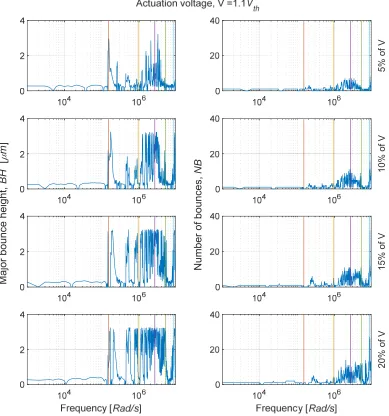
Chapter 3 presents a transient dynamic analysis of a typical cantilever type MEM switch. Bouncing which is responsible for switch performance degradation is illustrated. Performance parameters that describe the bouncing behavior of the switch such as initial contact time, permanent contact time, major bounce height, and number of significant bounces have been introduced and quantified. In addition, effect of harmonic dither in actuation electrostatic voltage as well as harmonic perturbations in the secondary PZT actuator voltage on the bouncing behavior have been illustrated. Regions of improvement in the switch bounce behavior due to frequency and amplitude of the harmonic perturbations are also demonstrated.
Chapter 5 provides the mathematical models that describe the dynamic behavior of cantilever NEM switches which are actuated electrostatically or via Casimir force. In both models, surface effects, intermolecular forces and damping are considered. Based on the surface elasticity model and the generalized Young-Laplace equation, both surface stress and surface elasticity are incorporated in governing equations, while intermolecular forces are taken into consideration using quantum field theory. Damping has also been incorporated in the model with consideration of the rarefication effect. The idea of switchable Casimir-force devices is proposed for the purpose of paving a new way to operate a switch by purely altering the magnitude of the Casimir force.
Chapter 6 presents the bouncing dynamic analysis of a typical electrostatically actuated cantilever type NEM switch. Performance parameters similar to the ones described of MEM switches are also introduced. The influence of surface effects on the pull-in parameters has been studied considering the bouncing behavior under different vacuum pressures. For pure Casimir actuated switch, the bouncing dynamic response has also been studied. The influence of switching parameters on the bouncing behavior have also been presented for different vacuum pressure values.
21 CHAPTER 2
MODELING OF A MEM SWITCH
2.1 Introduction
In this chapter, mathematical models of cantilever beam-based MEM switches are derived to describe the bouncing dynamics. A model that includes a comprehensive set of interacting forces as multimodal interactions is employed to study the bouncing dynamics of micro-switches. For the purposes of capturing accurate bouncing dynamics, a more realistic asperity-based contact force which represents the nonlinear contact mechanics between the beam tip and the substrate has been developed. This model also incorporates a squeeze-film damping force based on a modified Reynolds’ equation. An electrostatic actuation force with consideration of the fringing effect has also been incorporated in the model. In addition to these forces, an induced moment due to the piezoelectric layer effect has also been formulated and further incorporated in the equation of motion of an alternative switch model with combined actuation. Euler-Bernoulli beam theory is utilized to formulate the equation of motion that governs the switch dynamics. For response predictions, natural frequencies and mode shapes of the cantilever beam are evaluated and then an approximate numerical approach based on Galerkin’s method is employed, since closed-form solutions are not achievable in such nonlinear systems.
2.1 Equations of motion for a switch under electrostatic actuation
The MEM switch is generally modelled as a cantilever beam or a clamped-clamped beam. In the current work, a typical micro switch device which has a cantilever configuration of
length 𝐿, beam tip gap 𝑑 , beam initial gap 𝑑 , beam thickness 𝑏 , beam tip length 𝐿 , and
beam width 𝑎 as shown in Figure 2.1 is employed. In this configuration, an electrostatic
force is used to actuate this switch. When sufficient voltage 𝑉 is applied via an electrode
of length 𝐿 𝐿 , an electrostatic force is generated, and the beam is pulled down to make
cannot be ignored, and hence, a modified Reynolds’ equation is employed to formulate the damping force. Further, the contact boundary condition is also included using an asperity-based contact model which is more realistic when compared with linear spring models. The material for the switch is assumed to be as isotropic and homogeneous.
Euler-Bernoulli beam theory is used to develop the equation of motion that governs the flexural dynamics of the switch. When the electrostatic force, air-damping force, and the
contact force are incorporated in the modeling, the equation takes the form (Tung et al.,
2014):
𝐸𝐼 𝑥 , 𝜌𝐴 𝑥 , 𝑓 𝑓 𝑓 , (2.1)
where 𝑦 𝑥, 𝑡 is the transverse displacement of the beam. 𝐸 is the Young’s modulus and 𝜌
is beam material mass density per unit volume, while 𝐴 , 𝐼, respectively, denote the area
and moment of inertia associated with the beam’s cross-section. 𝑓 represents the actuation
electrostatic force while 𝑓 and 𝑓 , respectively, denote the squeezed-film damping force
and the contact force. It may be noted that all applied forces are expressed per unit length of the beam. The detailed expressions for these forces are discussed in the following sections
23 2.1.1 Electrostatic force
When a voltage 𝑉 is applied between the two electrodes of the switch, an electrostatic force
is generated, which is equivalent to applying a distributed transverse load to the movable electrode. Ideally the electrostatic field is uniform between the opposite electrodes; however, a uniform electrostatic field cannot drop to zero abruptly at the edges of the electrodes, and a “fringing field” always exists in a real situation. With the consideration
of the fringing effect, the electrostatic force per unit length of the beam is denoted by 𝑓
and it takes the following form (Bao, 2001):
𝑓 𝜀 𝑉 𝑎
2ℎ 1 𝛽 𝐻 𝑥 𝐿 𝐻 𝑥 𝐿 . (2.2)
The parameter 𝜀 denotes the permittivity of air, 𝑉 represents the applied voltage between
the electrode and the beam, ℎ 𝑑 𝑦, and 𝛽 represents the fringe effect correction
coefficient. The function, 𝐻 𝑥 , denotes the Heaviside step function, and the electrostatic
force is considered to act on the beam segment between lengths 𝐿 and 𝐿 . The fringe effect
correction coefficient takes the following form (Bao, 2001):
𝛽 ℎ
𝜋𝑎 ln 𝜋𝑎
ℎ ℎ
𝜋𝑎 ln 1 2𝑏
ℎ 2
𝑏 ℎ
𝑏
ℎ . (2.3)
2.1.2 Squeeze-film damping force
damping force. A simplified form of the Navier–Stokes equation, the Reynolds equation, has been employed to derive the squeeze-film damping pressure due to the air film between the beam and the substrate. Reynolds equation assumes that the effects of inertia are small compared to those of viscosity and pressure forces in the fluid film. The motion of the beam is assumed to be in the transverse direction such that surfaces of the beam and substrate approaching normally. For this type of relative motion, the beam sliding velocity is equal to zero and the Reynolds equation can be reduced to
𝜕 𝜕𝑥 𝜌ℎ 12𝜇 𝜕𝑃 𝜕𝑥 𝜕 𝜕𝑧 𝜌ℎ 12𝜇 𝜕𝑃 𝜕𝑧 𝜕 𝜌ℎ
𝜕𝑡 , (2.4)
where 𝜇 denotes the air viscosity that takes a value of 1.86 10 𝑁. 𝑠/𝑚 at 30 𝐶 and
𝜌 is the density of air. The air gap between the beam and the substrate is denoted by ℎ
where ℎ 𝑑 𝑦. When 𝜌 and 𝜇 are constant throughout the fluid and assuming that ℎ is
independent of z, this equation can be further simplified by assuming that the pressure, 𝑃 𝑥, 𝑧 , is a separable function in 𝑥 and 𝑧 directions and takes a parabolic shape in the
z-direction. Further, the thin film pressure 𝑃 consists of the ambient atmospheric pressure 𝑃
and the dynamic pressure ∆𝑃 as given below:
𝑃 𝑥, 𝑧 𝑃 ∆𝑃 𝑃 𝑃 𝑥 1 4𝑧
𝑎 . (2.5)
Use of non-dimensional quantities 𝑥̅ 𝑥/𝐿, ℎ ℎ/ℎ and 𝑎 𝑎/ℎ where ℎ is the
initial air gap between the beam and the substrate and substitution of Eq. (2.5) into Eq. (2.4), yield the following equation:
3 ℎ ℎ 𝐿 𝜕ℎ 𝜕𝑥̅ 𝜕𝑃 𝑥̅ 𝜕𝑥̅ 1 4𝑧 𝑎 ℎ ℎ 𝐿 𝜕ℎ 𝜕𝑥̅ 𝜕 𝑃 𝑥̅ 𝜕𝑥̅ 1 4𝑧 𝑎 8ℎ 𝑃 𝑥̅
𝑎 12𝜇
𝜕ℎ 𝜕𝑡 ,
(2.6)
Since ℎ ≪ 𝐿, Eq. (2.6) can be simplified by neglecting terms of order and the
25
𝑃 𝑥 12𝜇 𝑎
8ℎ 𝜕ℎ
𝜕𝑡 12𝜇
𝑎 8ℎ
𝜕ℎ
𝜕𝑡 . (2.7)
Thus, the squeeze film force per unit length is
𝑓 𝑃 𝑥 1 4𝑧
𝑎 𝑑𝑧
/
/
𝜇𝑎 ℎ
𝜕ℎ
𝜕𝑡 . (2.8)
2.1.3 Contact force
The first statistical elastic contact model of rough surfaces was presented by Greenwood and Williamson (1966). In this model, the contact of two rough surfaces is equivalently treated as the contact between a smooth plane and a nominally flat surface with some roughness profile. Contact between individual asperities was assumed to deform elastically according to Hertz theory. The heights of the asperities vary randomly and are defined by
a Gaussian height distribution function 𝜙 𝜉 , where 𝜉 denotes the asperity height.
Asperities are spherical near their summits and all asperity summits have the same radius
R; and are sufficiently separated to be mechanically independent. There is no bulk
deformation and only the asperities deform during contact. Fig 2.2 shows the model of such contacting rough surfaces. Hence, the force upon contact can be formulated as follows:
𝜂 𝐴 𝑃 𝑤 𝜙 𝜉 𝑑𝜉 , (2.9)
where 𝜂 is the area density of asperities, 𝐴 represents the nominal contact area,
𝜙 𝜉 denotes the asperity height distribution function, while 𝑤 𝜉 𝑦 𝑑 . The
applied load for a single asperity based on Hertzian contact theory is represented by 𝑃 𝑤
(Greenwood & Williamson, 1966):
𝑃 𝑤 𝐸∗𝑅 𝑤 , (2.10)
1 𝐸∗
1 𝑣
𝐸
1 𝑣
𝐸 . (2.11)
In Eq. (2.10), 𝑃 represents the applied load while 𝑅 and 𝑤, respectively, denote the radius
of the spherical asperity and the contact interference. The equivalent Young’s modulus 𝐸∗
is based on the Young’s moduli 𝐸 , 𝐸 and the Poisson’s ratios 𝑣 , 𝑣 of the two contact
surfaces. Since the asperity height distribution is Gaussian, therefore 𝜙 𝜉 can be
formulated as:
𝜙 𝜉 𝑒 , (2.12)
where 𝑀 denotes the mean value of the asperity height, while 𝜎 represents the variance
of the asperity height.
Theoretically, the assumed height distribution implies that the height of the asperities can be infinity. This assumption is not practical for dynamic studies since impacting bodies (surfaces) must have a clear boundary before and after contact. In other words, no force acts on the surfaces before the contact is made. Wang (2009) modified this model to overcome this unrealistic dynamic situation and proposed two simplified models based on the Greenwood-Williams model. A model with uniformly distributed asperity height and identical radii and another model with a Gaussian asperity radius distribution and asperity height are equal to the asperity radius or equal to a fixed value whichever is less. Simulations of the above two models carried out by Wang (2009) revealed that both models provide more realistic situation since the contact force becomes zero for zero interference