A High Efficiency Power Factor Correction Scheme
Based AC/DC Converter fed PMDC Drive
M.Kannan1, G.Neelakrishnan2, S.Selvaraju3
1,2Assistant Professor, Department of Electrical and Electronics Engineering 3
Assistant Professor, Department of Electronics and Communication Engineering 1,2,3Muthayammal College of Engineering, Namakkal, Tamilnadu.
[email protected], [email protected], [email protected]
Abstract— A new power factor correction scheme based on ac to dc flyback converter fed PMDC motor is presented in this paper. In the proposed circuit, the efficiency and power factor is improved by using an auxiliary (third) winding coupled to the transformer secondary of a dc to dc flyback converter. The flyback converter is placed between the input diode rectifier and drive as PMDC motor. Where the dc to dc flyback converter is operated at very high switching frequency and produces a high frequency pulsating source, so that input current harmonics is reduced. It results in higher efficiency and power factor. This circuit is not required to use of control circuit for power factor correction. In circuit input inductor is designed to operate in discontinuous current mode to get lower harmonic content.
Index Term s— AC to DC flyback converter, power factor, power factor correction, PMDC motor.
1. INTRODUCTION
The existing system power converters with diode rectifiers have resulted in distorted input current waveforms with high harmonic contents. A two-stage scheme results in high power factor and fast response output voltage by using two independent controllers and optimized power stages. The main drawbacks of this scheme are its relatively higher cost and larger size resulted from its complicated power stage topology and control circuits, particularly in low power applications. In order to reduce the cost, the single-stage approach, which integrates the PFC Stage with a dc/dc converter into one stage, is developed. It is shown in figure 1.
Fig.1 Typical single stage PFC converter
These integrated single-stage power factor correction (PFC) converters usually use a boost converter to achieve PFC with discontinuous current mode (DCM) operation. Usually, the DCM Operation gives a lower total harmonic distortion (THD) of the input current compared to the continuous current mode (CCM). However, the CCM operation yields slightly higher efficiency compared to the DCM operation.
Generally, single-stage PFC converters meet the regulatory requirements regarding the input
power factor and reduce the THD as much as their conventional two-stage counterpart. The power factor could be as low as 0.8, however, they still meet the regulation. In addition, although the single-stage scheme is especially attractive in low cost and low power applications due to its simplified power stage and control circuit, major issues still exist, such as low efficiency and high as well as wide-range intermediate dc bus voltage stress. To overcome the disadvantages of the single-stage scheme, many converters with input current shaping have been presented, in which a high frequency ac voltage source (dither signal) is connected in series with the rectified input voltage in order to shape the input current. A new concept of quasi-active PFC is proposed to improve the efficiency of a single-stage converter by preventing the input current or voltage stress due the PFC cell from being added to the active switch.
The PFC circuit, operation principles, analysis and results of the proposed converter are presented in Section II. The simulation results are presented in Section III.
2. PROPOSED POWER FACTOR CORRECTION CIRCUIT
132
between rectifier and flyback converter. The PFC cell consists of L, C and auxiliary winding. This improves the power factor up to above 0.9.Where the dc to dc flyback converter is operated at high-switching frequency, the auxiliary windings produce a high frequency pulsating source, which results in the input current harmonics is reduced.
Fig.2 Block diagram of PFC
The Controller generates PWM signal for MOSFET switch used in flyback converter is fed to PMDC motor. The input inductor LB operates in
DCM such that a lower THD of the input current can be achieved. The proposed quasi-active PFC circuit is analyzed in this section. As shown in Fig.3, the circuit comprised of a bridge rectifier, a boost inductor LB, a bulk capacitor Ca in series with the auxiliary windings L3, an intermediate dc-bus voltage capacitor CB, and a discontinuous input current power load, such as flyback converter. The flyback transformer (T) has three windings N1, N2, and N3. The secondary winding N2 = 1is assumed. In the proposed PFC scheme, the dc/dc converter section offers a driving power with high-frequency pulsating source. The quasi active PFC cell can be considered one power stage but without an active switch. All the capacitors are high enough so that the voltage across them is considered constant.
2.1Principles of Operation of the Proposed Circuit
To facilitate the analysis of operation, Fig. 4(a) and (b) shows the topological stages and the key waveforms of the proposed circuit. It is assumed that both the input inductor LB and the magnetizing inductance of the flyback converter operate in DCM. Therefore, currents iLB, im, and i2 are zero at the beginning of each switching period. It is also assumed that the average capacitor voltage VCa is greater than the average rectified input voltage |vin |. To ensure proper operation of the converter, the Transformer’s turn’s ratio should be (N1/N3) ≥ 2
and the boost inductor LB < Lm. In steady-state operation, the topology can be divided into four operating stages.
1) Stage 1 (to − t1): When the switch (SW) is
turned on at t = to, diodes D1 and Do are OFF, therefore, the dc-bus voltage VCB is applied to the magnetizing inductor Lm, which causes the magnetizing current to linearly increases. This current can be expressed as
And since diode D1 is OFF, the input inductor LB is charged by input voltage, therefore, the inductor current iLB is linearly increased from zero since it is assumed that the PFC cell operates in DCM. At this stage, iLB = −i3 and the capacitor Ca is in the charging mode. On the other hand, Do is reversed biased and there is no current flow through the secondary winding. Since the transformer is assumed ideal, based on Ampere’s Law, it has
N1 i1 + N2 i2 − N3 iLB = 0
Fig.3 Proposed PFC circuit diagram
2) Stage 2 (t1 − t2): When the switch is turned
OFF at t = t1, output diode Do begins to be forward biased. Therefore, the energy stored in the transformer magnetizing inductor is delivered to the load through the secondary winding. Similarly, the diode D1 is also forward biased and the voltage across LB now Vin − VCB. Therefore, the current
ILB is linearly decreased to zero at t = t2 (DCM
operation), and the energy stored in LB is delivered to the dc bus capacitor CB . Therefore
The capacitor (Ca ) is also discharging its energy to the dc bus capacitor CB and the current i3 reverse its direction. Therefore, the capacitor current is given by
iD1 = iCB = iLB + i3
3) Stage 3 (t2 − t3): At this stage, the input
inductor current iLB reaches zero and the capacitor
Ca continues to discharge its energy to the dc bus
capacitor CB. Therefore, iD1 = iCB = i3. At t = t3 , the magnetizing inductor releases all its energy to the load and the currents im and i2 reach to zero level because a DCM operation is assumed.
4) Stage 4 (t3 − t4): This stage starts when the
currents im and i2 reach to zero. DiodeD1 still forward biased, therefore, the capacitor Ca still releasing its energy to the dc bus capacitor CB. This stage ends when the capacitor Ca is completely discharged
Fig.4 Equivalent circuit operation stages of the proposed PFC circuit during one switching period
3. EXPERIMENTAL VERIFICATION
In order to verify the proposed concept, a prototype of the converter shown in Fig.3 was constructed and experimentally tested. To ensure proper operation of the converter, the dc bus voltage (VCB) must be higher than the input voltage, such that the diode D1 is OFF and the inductor LB stores energy when the switch (SW) is ON. Therefore, the inductor Lm must be higher than the input inductor
LB. The DCM flyback converter was designed and implemented for 50 V/80 W output,
The major components of the circuit are follows: transformer turns ratio (N1 = 30,N2 =
134
sinusoidal waveform and it meets the regulation standards. Fig. 5 shows the DC to DC Flyback converter circuit.
Fig.5 DC to DC Flyback Converter Circuit
Fig.6 Measured harmonics content of the input current
4. SIMULATION CIRCUIT
The Simulink model for the proposed quasi active PFC with ac/dc converter is given in the Fig.7. A 230V AC voltage is given as the input to the rectifier. The circuit consists of INPUT rectifier along with a three winding linear transformer. The AC source power factor is improved in simulation circuit.
Fig.7 Simulation circuit of the proposed quasi active PFC
5. OUTPUT WAVEFORMS
From fig.8 it clearly shows that the power factor has been improved. The proposed PFC converter gives power factor about 0.987 and also harmonics are reduced. It shows the fig.9.
Fig-8 Power factor waveform
Fig.10 Converter Output voltage Waveform
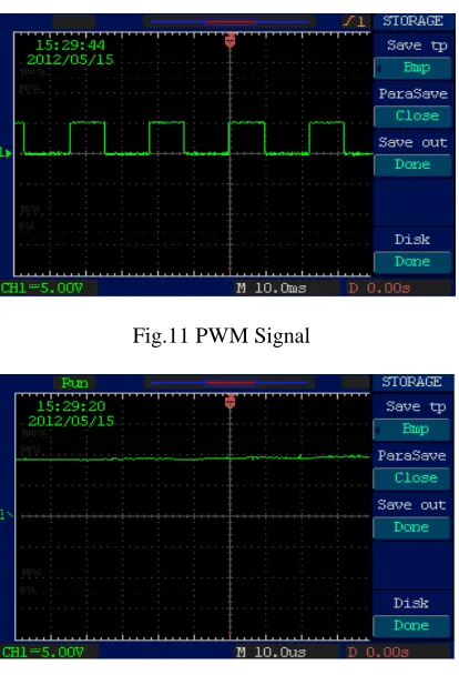
Fig.11 PWM Signal
Fig. 12 Converter Output voltage Waveform
6. CONCLUSION
In this paper, a new ac/dc converter based on a quasi-active PFC scheme has been presented. The proposed method produces a current with low harmonic content to meet the standard specifications as well as high efficiency. This circuit is based on adding an auxiliary winding to the transformer of a cascade dc/dc DCM flyback converter. The input inductor can operates in DCM to achieve lower THD and high power factor. By properly designing the converter components, a trade off between efficiency and harmonic content can be established to obtain compliance with the regulation and efficiency as high as possible. Operating principles, analysis, and experimental results of the proposed method are presented.
[1] O. Gracia, J. A. Cobos, R. Prieto, and J. Uceda, “Single-phase power factor correction: A survey,” IEEE Trans. Power Electron., vol. 18, no. 3, pp. 749–755, May 2003.
[2] R. Redle, L. Balogh, and N. O. Sokal, “A new family of single-stage isolated power factor correctors with fast regulation of the output voltage,” in Proc. IEEE PESC 1994 Conf., pp. 1137–1144.
[3] C. Qian and K. Smedley, “A topology survey of single-stage power factor with a boost type input current-shaper,” IEEE Trans. Power
Electron., vol. 16, no. 3, pp. 360–368, May
2001.
[4] T.-F. Wu, T.-H. Yu, and Y.-C. Liu, “An alternative approach to synthesizing single-stage converters with power factor correction feature,” IEEE Trans. Ind. Electron., vol. 46, no. 4, pp. 734–748, Aug. 1999.
[5] L. Huber, J. Zhang, M. Jovanovic, and F.C. Lee, “Generalized topologies of single-stage input-current-shaping circuits,” IEEE Trans.
Power Electron, vol. 16, no. 4, pp. 508–513,
Jul. 2001.
[6] H. Wei, I. Batarseh, G. Zhu, and K. Peter, “A single-switch AC-DC converter with power factor correction,” IEEE Trans. Power
Electron., vol. 15, no. 3, pp. 421–430, May
2000.
[7] L. K. Chang and H. F. Liu, “A novel forward AC/DC converter with input current shaping and fast output voltage regulation via reset winding,” IEEE Trans. Ind. Electron., vol. 52, no. 1, pp. 125–131, Feb. 2005.
[8] H. L. Do, “Single-stage single-switch power factor correction AC/DC converter,” Inst.
Electr. Eng. Proc. Electr. Power Appl., vol.
152, no. 6, pp. 1578–1584, Nov. 2005.
[9] J. Qian, Q. Zhao, and F. C. Lee, “Single-stage single-switch power factor correction ac/dc converters with dc-bus voltage feedback for universal line applications,” IEEE Trans.
Power Electron., vol. 13, no. 6, pp. 1079–
1088, Nov. 1998.
[10] S. Luo,W. Qiu,W.Wu, and I. Batarseh, “Flyboost power factor correction cell and a new family of single-stage AC/DC converters,” IEEE Trans. Power Electron., vol. 20, no. 1, pp. 24–33, Jan. 2005.
[11] M. M. Jovanovic, D. M. Tsang, and F. C. Lee, “Reduction of voltage stress in integrated high-quality rectifiers-regulators by variable frequency control,” in Proc. IEEE
APEC 1994 Conf., pp. 569– 575.