36
B. Maheswara Rao
1, G.Sreenivasa Rao
21
Department of Electronics and communication engineering Khammam Institute of Technology & sciences
Jawaharlal Nehru Technological University, Andhra Pradesh, India 2
Department of Electronics and communication engineering GUNTUR Engineering college,
Jawaharlal Nehru Technological University, Andhra Pradesh, India 1Email: [email protected]2
ABSTRACT
This paper describes the design of FPGA based signal processing card. An on board real time digital signal processing system is designed using FPGA. The platform can decode process of various kinds of digital and analog signals simultaneously. The design trend in this card is towards small size, high integration and fast real time processing. For the optimum performance a 16 bit 1 MSPS ADC is used which is interfaced with FPGA to make all the data processing onboard in real time. This card can be used in many signal processing based applications like audio signal processing, audio compression, digital image processing, video compression, speech processing, speech recognition, digital communications by interfacing several separate board using inbuilt I/O’s, each with a number of input channels that will communicate with each other in real time over a high speed communication link. The resulting images can be displayed directly on LCD or OLED panel displays using I/O’s peripherals. The project introduces many challenging issues, which are being addressed in turn with different prototype design. These issues are the ADC performance, interfacing the ADCs to the FPGA, implementing the flexible processing algorithms and high speed interconnection between the boards.
Keywords –
Xilinx New version, mentor graphics, EDA-Tools.1.
INTRODUCTION
Digital hardware is generally superior and more reliable than its analogue counterpart which can be prone to ageing and can give uncertain performance in production. DSP on the other hand gives a guaranteed accuracy and essentially perfect reproducibility. In addition, there is considerable interest in merging the multiple networks that transmit these signals; this provides a strong motivation to convert a wide range of information formats into their digital formats. Microprocessors, DSP micros and FPGAs perform a suitable platform for processing such digital signals, more recently, the field-programmable gate array (FPGA) has been proposed as a hardware technology for DSP systems in many new designs and applications For a variety of reasons but primarily because of their extreme-high performance and flexibility. This is particularly true now that FPGAs have integrated gigabit serial communications, memory interfaces, immersed processors, and a wide range of available core firmware modules .
This card is tested for laser beam communication which requires very fast data processing although it can also be used for a vast range of signal processing’s simultaneously. For that purpose a high speed system is being developed that not only delivers high performance, but also a high degree of flexibility that is not commercially available. To limit energy in a reasonable size battery, minimum power dissipation in the mixed-signal integrated circuits is necessary. The analog-to-digital converter (ADC) is the key component because it bridges the gap between the analog physical world and digital logic world.
2.
DEVELOPMENT
STRATEGY
The main concept is that by using A/D converter we can maintain the good energy and time resolution. We are using AD7671 ADC with 16-bit resolution, 1 MSPS, charge redistribution SAR, analog-to-digital converter
37
that operates from a single 5 V power supply. It contains a high speed 16-bit sampling ADC, a resistor input
scalar that allows various input ranges, an internal conversion clock, error correction circuits, and both serial and parallel system interface ports. For superior performance and highest flexibility, a PROM flash memory LHF00L28 (16Mbit- 1MX16 with a read operation of 70ns) externally connected to the FPGA. Is used for storing the data, allowing the implementation of high performance signal processing tasks. Resulting images can be displayed directly on LCD or OLED panel displays using me /O’s peripherals. In this FPGA, volatile memory devices can also be programmed via the JTAG port normally during development work. In addition, newer parts, for instance Xilinx Virtex-4, have internal monitoring capability (temperature, voltage and current) accessible via the JTAG port.
Connecting the peripherals to a logic analyzer
The first step to evaluate an RS232, OLED, GPIOs, ADC and memories that could be suitable for our design, was to connect the evaluation board to a logic analyzer through custom designed adapter boards. Data from the logic analyzer was transferred to a computer using hypertext terminal for offline processing. After checking the functionality of all these peripherals which are required for developing the signal processing system, are being used.
Development and interfacing of FPGA with ADC, flash memory
The second step was to develop a prototype board with a Virtex-4SX FPGA to interface with ADC, Memory RS232, Power Supply, OLED and GPIOs. For interfacing these peripherals their Drivers has to be made, hence VHDL coding is used for making drivers. The bit file generated after coding is burned in PROM memory of FPGA. After the proper interfacing all the peripherals are tested and their responses are adjusted accordingly. Therefore the outcome is a adaptive hardware that continuously change in response to the input data, the design trends in this card are towards small size, high integration and fast real time processing.
3.
SIGNAL
PROCESSING
SYSTEM
This FPGA based signal processing card is compatible for both types of signals, digital as well as analog. This card uses FFT, it gives capability to accelerate and verify their real time signal processing design. The new stem signal processing kit radically reduces simulation time and simplifies the overall design process. The tool allows designer to easily incorporate their FPGA hardware directly into the impact tool using a JTAG interface.
By using push button a designer can automatically generate a FPGA bit stream from the tool and incorporate the FPGA back into the system level simulation .this card also gives a tremendous choice of FPGA based boards to target a unique capability. The AD7671 has a maximum integral nonlinearity of 2.5 LSB with no missing 16-bit code.ADC output samples stored in 16 bit flash memory i.e. LHF00L28 IC .Flash memory used to store multiple samples which are coming from LASER beam through ADC. After the comparison of different samples the effective data pass through the DDS interface.
4.
PROTOTYPE
BOARD
38
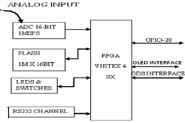
Figure1: Block diagram of signal processing card
Block diagram of signal processing card which is shown in Figure.1, the FPGA interfaced with I/O and other peripheral device. As far as our card specification is concerned:
Area of the PCB - 70mX130m Execution time- 200ms Power consumption- 40mw
Input signal- various analog signals ranging from 10mv to 30mv as well as digital signals. Tested for LASER beams incident on a photo diode.
[image:3.595.137.456.130.343.2]5.
RESULT AND DISCUSSION
Figure 2: PCB Design steps
39
6.
WORKING
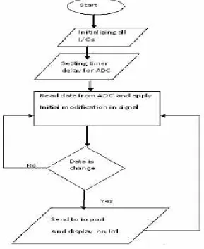
[image:4.595.157.446.238.591.2]The following flow chart shows the working of signal processing card (Figure.4), first the FPGA is initialized for all I/O peripherals. Then analog data is applied to the ADC in the form of LASER beam, where it gets converted to digital form and stored in FLASH memory. This digital signal is then retrieved and processed by FPGA and synthesized by DDS interface, the o/p of this stage is noise free analog signal. This analog signal is then compared with the previous analog signal and is checked for noise removal. If the noise has been removed the signal is transferred to the display. If there is no change in the compared signal then it is again send for processing and synthesizing.
Figure 3: Working of signal processing card
7.
CONCLUSION
40
simultaneously depending upon the need, this shows the processing of signal at a high speed . FPGA based
platform is addressing the problems by allowing add-on cards to meet application-specific feature and performance requirements.
R
EFERENCES[1] Attila Hidvegi et.al.”A High Speed Data Acquisition System for Segmented GE-Detectors”, IEEE, 2006
[2] A.Hidvegi et al., A High-Speed Data Acquisition System for Segmented Ge-Detectors, IEEE Nuclear Science Symposium Conference Proceedings, (2006) ISSN: 1082-3654
[3] Hitachi HD44780U (LCD-II) Dot Matrix Liquid Crystal Display Controller/Driver Datasheet, Revision 0.0. Hitachi Ltd.
[4] Kung SY VLSI Array Processors. Prentice Hall
[5] DeHon A Dynamically programmable gate arrays: A step toward increased computational density. [6] http://www.latticesemi.com/documents/doc26686x11.pdf
[7] http://www.eetimes.com/design/programmable-logic/ 4014823/
[8] http://www.xilinx.com/publications/archives/solution guides/ memory interfaces.pdf [9] http://e2e.ti.com/support/data converters/ high speed data converters /f /68/ t /102548.aspx [10] http://wenku.baidu.com/view/2b6ffffc910ef12d2af9e7f5.html
[11]http://www.mentor.com/products/pcb-system-design/blog/post/pcb-design-perfection-starts-in-thecad- library-part-19-e2558ae4-04e4- 42c6-94f5-31207e92ffd1
[12]http://www.mentor.com/products/pcb-system-design/blog/tag/hyperlynx-c3befda1-74cf-49b4-8d49-22bb460766e4 [13] http://www.docstoc.com/docs/26451369/Mentor-Graphics-PCB-Layout-Tips
About Author.1
Mr. BHUKYA MAHESWARA RAO, He has completed his B.Tech in ECE from – Sri Raja Rajeswari Engineering College-Karepally Khammam (JNTUH) in 2006 and M.Tech(VLSISD)-From Hyderabad Institute of Technology & Management (JNTUH)in 2010. Now Pursuing Ph.D in COMMUNICATION ENGINEERING from VEL TECH TECHNICAL UNIVERSITY. Avadi, Chennai. His interested areas are Digital Design, Low Power VLSI Design, Analog VLSI Design, FPGA Technology and wireless communications.