Design of Low Power Adder and Multiplier Using Reversible
Logic Gates
M.Veerendra Kumar
P1
P
, K.Prasad Babu
P2
P
S.Ahmed Basha
P3 P
H.Devanna
P 4 PK.Sudhakar
P 5 P 1 , PMtech VLSISD 13G31D5710, ECE, JNTUA/SJCET,
Yerrakota kurnool, Andhra Pradesh 518360, India, [email protected]
P
2
P
Assistant Professor ECE, JNTUA/SJCET,
Yerrakota kurnool, Andhra Pradesh 518360, India, 31TU[email protected]U31T
P
3
P
Assistant Professor ECE, JNTUA/SJCET,
Yerrakota kurnool, Andhra Pradesh 518360, India, [email protected]
P
4
P
Associate Professor ECE, JNTUA/SJCET,
Yerrakota kurnool, Andhra Pradesh 518360, India, [email protected]
P
5
P
Associate Professor & HOD ECE dept, JNTUA/SJCET,
Yerrakota kurnool, Andhra Pradesh 518360, India, [email protected]
Abstract
In this project reversible logic gates are designed. Reversible logic is a prominent technology in Quantum computing technology. The devices used by this technology operate at ultra high speed and consume very low power. In this work basic reversible logic gates are implemented using hardware description language. The Wallace tree multiplier is implemented using basic half adder and full adder using verilog. GCD processor is also implemented using verilog. The reversible logic gates are designed and a 4bit reversible adder, irreversible adder along multiplier is designed. Various foundry technologies are used for the design of layouts and comparison among these technologies is done. The least power dissipation technology is concluded
.
In this paper a 4x4 bit reversible multiplier circuit is proposed and designed. The proposed reversible multiplier is faster and has lower hardware complexity compared to the existing counterparts. It is also better than the existing counterparts in term of number of gates, garbage outputs and constant inputs. Haghparast and Navi recently proposed a 4x4 reversible gate called "HNG". The reversible HNG gate can work singly as a reversible full adder. In this paper we use HNGgates to construct the reversible multiplier circuit. The proposed reversible multiplier circuit using HNG gate can multiply two 4-bits binary numbers. The proposed reversible 4x4 multiplier circuit can
be generalized for NxN bit multiplication.
Keywords:
Reversible gates, Power Dissipation,Verilog, Adder, Multiplier
1.
Introduction
Reversible computing was started when the basis of thermodynamics of information processing was shown that conventional irreversible circuits unavoidably generate heat because of losses of information during the computation . The different physical phenomena can be exploited to construct reversible circuits avoiding the energy losses. One of the most attractive architecture requirements is to build energy lossless, small and fast quantum computers. Most of the gates used in digital design are not reversible for example NAND, OR and EXOR gates.
A Reversible circuit/gate can generate unique output vector from each input vector, and vice versa, i.e., there is a one to one correspondence between the input and output vectors. Thus, the number of outputs in a reversible gate or circuit has the same as the number of inputs, and commonly used traditional NOT gate is the only reversible gate. Each Reversible gate has a cost associated with it called Quantum cost. The Quantum cost of a Reversible gate is the number of 2*2 Reversible gates or Quantum logic gates required in designing. One of the most important features of a Reversible gate is its garbage output i.e., every input of the gate which is not used as input to other gate or as a primary output is called garbage output.
In digital design energy loss is considered as an important performance parameter. Part of the energy dissipation is related to non-ideality of switches and materials. Higher levels of integration and new fabrication
processes have dramatically reduced the heat loss over the last decades. The power dissipation in a circuit can be reduced by the use of Reversible logic. Landauer’s [2] principle states that irreversible computations generates heat of K*Tln2 for every bit of information lost, where K is Boltzmann’s constant and T the absolute temperature at which the computation performed. Bennett [3] showed that if a computation is carried out in Reversible logic zero energy dissipation is possible, as the amount of energy dissipated in a system is directly related to the number of bits erased during computation. The design that does not result in information loss is irreversible.
A set of reversible gates are needed to design reversible circuit. Several such gates are proposed over the past decades. Arithmetic circuits such as Adders, Sub tractors, Multipliers and Dividers are the essential blocks of a Computing system. Dedicated Adder/Sub tractor circuits are required in a number of Digital Signal Processing applications. Several designs for binary Adders and Sub tractors are investigated based on Reversible logic. Minimization of the number of Reversible gates, Quantum cost and garbage inputs/outputs are the focus of research in Reversible logic.
Pawel Kerntopf [20] explained multipurpose Reversible gates and example of efficient binary multipurpose reversible gates. Thapliyal and Ranganathan [5] proposed the design of Reversible Binary Sub tractor using TR Gate. The particular function like Binary Subtraction is implemented using TR gate effectively by reducing number of Reversible gates, Garbage outputs and Quantum Cost. Thapliyal and Ranganathan [6] presented a design of Reversible latches viz., D Latch, JK latch, T latch and SR latch that are optimized in terms of quantum cost, delay and garbage outputs. Lihui Ni et al., [7] described general approach to construct the Reversible full adder and can be extended to a variety of Reversible full-adders with only two Reversible gates. Irina Hashmi and Hafiz Hasan Babu [8] designed an efficient reversible barrel shifter which is capable of left shift/rotate used for high speed ALU applications.
Robert Wille et al., [9] explored two techniques from irreversible equivalence checking applied in the reversible circuit domain. (i) Decision diagram Technique equivalence checking for quantum circuits and (ii) Boolean satifiability checking for garbage input/outputs. Noor Muhammed Nayeem et al., [10] presented designs of Reversible shift registers such as in out, in parallel-out, parallel-in serial-out, parallel-in parallel-out and universal shift registers. Majid Mohammadi, Mohammad Eshghi et al., [11] proposed a synthesis method to realize a Reversible Binary Coded Decimal adder/subtractor circuit. Genetic algorithms and don’t care concepts used to design and optimize all parts of a Binary Coded Decimal adder circuit
in terms of number of garbage inputs/outputs and quantum cost.
Majid Mohammadi and Mohammad Eshghi [12] explained about the behavioral description and synthesis of quantum gates. To synthesize reversible logic circuits, V and V+ gates are shown in the truth table form and shown that bigger circuits with more number of gates can be synthesized. Rekha James et al.,[13] proposed an implementation of Binary Coded Decimal adder in Reversible logic, which is basis of ALU for reversible CPU.
VLSI implementations using one type of building block can decrease system design and manufacturing cost. Himanshu Thapliyal and Vinod [14] presented the Transistor realization of a new 4*4 Reversible TSG gate. The gate alone operates as a Reversible full adder. The Transistor realizations of 1-bit Reversible full adder, ripple carry adder and carry skip adder are also discussed. Himanshu Thapliyal and Srinivas [15] proposed a 3x3 Reversible TKS gate with two of its outputs working as 2:1 multiplexer. The gate used to design a Reversible half adder and further used to design multiplexer based Reversible full adder. The multiplexer based full adder is further used to design Reversible 4x4 Array and modified Baugh Woolley multipliers
Yvan Van Rentergem and Alexis De Vos [16] presented four designs for Reversible full-adder circuits and the implementation of these logic circuits into electronic circuitry based on C-MOS technology and pass-transistor design. The chip containing three different Reversible full adders are discussed. Mozammel Khan [17] proposed realizations of ternary half and full-adder circuits using generalized ternary gates. Mozammel Khan
[18] discussed quantum realization of ternary Toffoli gate which requires fewer gates than the existing literature. Abhinav Agrawal and Niraj Jha [19] presented 6 the first practical synthesis algorithm and tool for Reversible functions with a large number of inputs. It uses positive-polarity Reed-Muller decomposition at each stage to synthesize the function as a network.
In digital design energy loss is considered as an important performance parameter. Part of the energy dissipation is related to non-ideality of switches and materials. Higher levels of integration and new fabrication processes have dramatically reduced the heat loss lover the last decades. The power dissipation in a circuit can be reduced by the use of reversible logic.
According to Landaulet’s principle states that irreversible computations generates heat of K*Tln2 for every bit of information lost, where K is Boltzmann’s constant and T the absolute temperature at which the computation performed. Bennett showed that if a computation is carried out in reversible logic zero energy dissipation is possible, as the amount of energy dissipated in a system is directly related to the number of bits erased during computation. The design that does not results in information loss is irrieversible. A set of reversible gates are needed to design reversible circuit. Several such gates are proposed over the past decades.
2.
Reversible logic gates
A reversible logic gate is an n-input n-output logic device with one-to-one mapping. This helps to determine the outputs from the inputs and also the inputs can be uniquely recovered from the outputs. Also in the synthesis of reversible circuits direct fan-Out is not allowed as one–to-many concept is not reversible. However fan-out in reversible circuits is achieved using additional gates. A reversible circuit should be designed using minimum number of reversible logic gates. From the point of view of reversible circuit design, there are many parameters for determining the complexity and performance of circuits.
Figure 1: Reversible Gate
A gate with k inputs and k outputs is called k*k gate. The gate/circuit that does not loose information is called reversible. The input vector and output vector of a reversible gate is as shown in equations (1) & (2).
Input Vector
IRk R=( IR1R , IR2R , IR3 R, … , IRk-1R, IRk R) . . . .(1)
Output Vector
ORk R=( OR1R , OR2R , OR3 R, … , ORk-1R, ORk R) . . .
.(2)
3.
Implementation of Reversible
Gates
Reversible computation is related to other emerging technologies such as quantum computation optical computing and nanotechnologies that use a similar or slightly extended set of gates.
First implementations and fabrications of reversible logic in CMOS technology have also been accomplished. These exploit that reversible logic is particularly suitable when it comes to reuse of signal energy (in contrast to static CMOS logic that sinks the signal energy with each gate), and, when using adiabatic switching to switch transistors in a more energy efficient way.
In fact, reversible circuits have shown that such implementations have the potential to reduce energy consumption by a factor. A drawback of these implementations comes from another law related to transistors, namely that the energy consumption is directly related to the execution frequency. If one performs many computations every second, the energy consumption per computation rises. Performing fewer computations lowers the energy consumption per computation. Of course, this implies that not all applications are necessarily suited for implementation using reversible circuits. However, many embedded devices do not need to perform billions of computations every second. In the rest of this section will focus on how to implement reversible gates in CMOS. First, we briey review some basics of CMOS transistor implementation as used in this work, and afterward we explain how this is used in an implementation of reversible gates. The following are various types of reversible gates
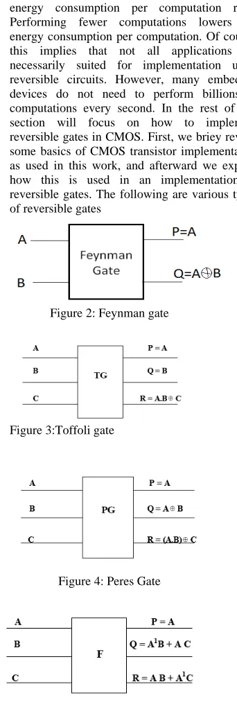
Figure 2: Feynman gate
Figure 3:Toffoli gate
Figure 4: Peres Gate
Figure 5: Fred kin gate
Figure 6: HNG gate
Figure 7: 4x4 reversible multiplier circuit using HNG gates and Peres gates The basic cell for such a multiplier is a full adder (FA) accepting three bits. We use HNG gates as reversible full adder which is depicted in Fig. 8. The proposed reversible multiplier circuit uses eight reversible HNG full adders. In addition, it needs four reversible half adders. It is possible to use HNG gate as half adder, but we use Peres gate as reversible half adder because it has less hardware complexity and quantum cost compared to the HNG gate.
Figure 8: reversible adder circuit using HNG gates
Figure 9: partial products in multiplier
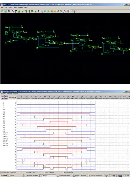
Figure 10: Reversible adder and its simulation.
Figure 11: Irreversible adder and its simulation.
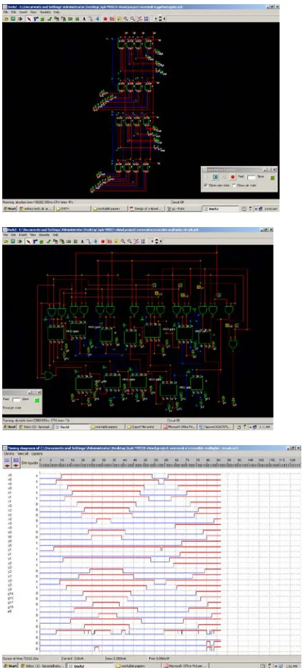
Figure 12: Reversible multiplier and its simulation
4.
Layout
Figure 13: Layout of Reversible multiplier
Figure 13: 250nm technology Reversible multiplier power dissipation
Figure 14: 120nm technology Reversible multiplier power dissipation
Figure 15: 90nm technology Reversible multiplier power dissipation
Figure 17: 45nm technology Reversible multiplier power dissipation
5.
Implementation of Wallace tree
multiplier and GCD processor:
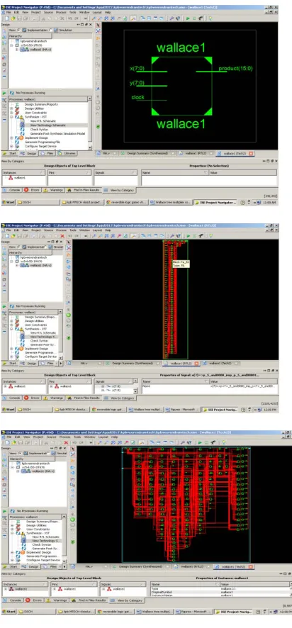
Figure 18: Wallace tree multiplier and GCD processor implementation using Verilog
6.
RESULTS
Table 1: Comparison of foundry technologies for reversible multiplier
Sl.No Technology Power Dissipation
1 250nm 4.35mW
2 120nm 63.235µW
3 90nm 16.856 µW
4 45nm 1.3µW
CONCLUSION & FUTURESCOPE
From Table 1, we conclude that using 45nm the reversible multiplier is having lower dissipation Power dissipation in multiplier designs has been much-researched in recent years, due to the importance of the multiplier circuit in a wide variety of microelectronic systems. The focus of multiplier design has traditionally been delay optimization, although this design goal has recently been supplemented by power consumption considerations. Our goal has been first to understand how power is dissipated in multipliers, and secondly to devise ways to reduce this power consumption. We have presented an investigation of multiplier power dissipation, along with some techniques which allow reductions in power consumption for this circuit. Given the importance of multipliers, it is likely that further research efforts will be directed at optimizing this block for delay and power efficiency. In this paper, we presented a novel 4x4 bit reversible multiplier circuit using HNG gates and Peres gates. Table 2 demonstrates that the proposed reversible multiplier circuit is better than the existing designs in terms of hardware complexity, number of gates, garbage outputs and constant inputs. Furthermore, the restrictions of reversible circuits were highly avoided. Our proposed reversible multiplier circuit can be applied to the design of complex systems in nanotechnology. All the proposed circuits are technology independent since quantum logic and optical logic implementations are not available.
REFERENCES
[1] C H Bennett, (1998) "Notes on the History of Reversible Computation", IBM Journal of Research and Development, vol. 32, pp. 16-23.
[2] R Landauer, (1961) “Irreversibility and Heat Generation in the Computational Process”, IBM Journal of Research and Development, vol. 5, no. 3, pp. 183-191.
[3] C H Bennett, (1973) “Logical Reversibility of Computation”, IBM Journal of Research and Development, vol. 17, no. 6, pp. 525-532.
[4] T Toffoli, (1980) “Reversible Computing”, Technical Memo MIT/LCS/TM-151, MIT Lab for Computer Science. [5] H Thapliyal and N Ranganathan, (2009) “Design of Efficient Reversible Binary Sub tractors Based on a New Reversible Gate”, IEEE Proceedings of the Computer Society Annual Symposium on VLSI, pp. 229-234. [6] H Thapliyal and N Ranganathan, (2010) “Design of Reversible Latches Optimized for Quantum Cost, Delay and Garbage Outputs”, Proceedings of Twenty Third International Conference on VLSI Design, pp. 235-240. [7] Lihui Ni, Zhijin Guan, and Wenying Zhu, (2010) “A General Method of Constructing the Reversible FullAdder”, Third International Symposium on Intelligent Information Technology and Security Informatics, pp. 109-113.
[8] Irina Hashmi and Hafiz Md. Hasan Babu, (2010) “An Efficient Design of a Reversible Barrel Shifter”, Twenty Third International Conference on VLSI Design, pp. 93-98. [9] Robert Wille, Daniel Grobe , D Michael Miller, and Rolf Drechsler, (2009) “Equivalence Checking of Reversible Circuits”, Thirty Ninth International Symposium on Multiple-Valued Logic, pp. 324-330.
[10] Noor Muhammed Nayeem, Md. Adnan Hossain, Lafifa Jamal, and Hafiz Md. Hasan Babu, (2009) “Efficient Design of Shift Registers using Reversible Logic”, International Conference on Signal Processing Systems, pp. 474-478.
[11] Majid Mohammadi, Mohammad Eshghi, Majid Haghparast and Abbas Bahrololoom, (2008) “Design and Optimization of Reversible BCD Adder/Sub tractor Circuit for Quantum and Nanotechnology Based Systems”, World Applied Sciences Journal, vol. 4, no. 6, pp. 787-792. [12] Majid Mohammadi and Mohammad Eshghi, (2008) “Behavioral description of V and V+ gates to Design Quantum Logic Circuits”, Fifth International Multi-Conference on Systems, Signals and Devices, pp. 1-6. [13] Rekha K James, Shahana T K, K Poulose Jacob, and Sreela Sasi, (2007) “A New Look at Reversible Logic Implementation of Decimal Adder”, The International Symposium on System-On-Chip.
[14] Himanshu Thapliyal and A P Vinod, (2006) “Transistor Realization of Reversible TSG Gate and Reversible Adder Architectures”, Proceedings of IEEE Asia Pacific Conference on Circuits and Systems, pp. 418-421.
[15] Himanshu Thapliyal and M B Srinivas, (2006) “Novel Design and Reversible Logic Synthesis of Multiplexer Based Full Adder and Multipliers”, Forty Eight Midwest Symposium on Circuits and Systems, vol. 2, pp. 1593 – 1596.