C
o m p u t i n g
S
u r f a c e
SPARC/IO Processing Element
(MK401) Users Guide
This document may not be copied, in whole or in part, without the prior written consent of Meiko World Incor-porated.
© copyright 1995 Meiko World Incorporated.
The specifications listed in this document are subject to change without notice.
Meiko, CS-2, Computing Surface, and CSTools are trademarks of Meiko Limited. Sun, Sun and a numeric suffix, Solaris, SunOS, AnswerBook, NFS, XView, and OpenWindows are trademarks of Sun Microsystems, Inc. All SPARC trademarks are trademarks or registered trademarks of SPARC International, Inc. Unix, Unix System V, and OpenLook are registered trademarks of Unix System Laboratories, Inc. The X Windows System is a trade-mark of the Massachusetts Institute of Technology. AVS is a tradetrade-mark of Advanced Visual Systems Inc. Verilog is a registered trademark of Cadence Design Systems, Inc. All other trademarks are acknowledged.
Circulation Control:
Meiko’s address in the US is:
Meiko
130 Baker Avenue Concord MA01742
508 371 0088 Fax: 508 371 7516
Meiko’s address in the UK is:
Meiko Limited 650 Aztec West Bristol
BS12 4SD
Tel: 01454 616171 Fax: 01454 618188
Issue Status: Draft Preliminary
Release x
1.
Overview . . . .
1
2.
MK401 Board Description . . . .
3
MBus. . . 5
ROSS Pinnacle Module . . . 5
Texas Instruments Viking Module . . . 6
SBus Interfaces . . . 8
Memory Configurations . . . 9
IO Bus . . . 10
Board Control Processor . . . 11
3.
Using the MK401. . . .
13
Installation . . . 13
Removing the Module’s Front Panel . . . 13
Installing the Processor Board . . . 14
Field Serviceable Components . . . 15
Installing MBus Processor Modules . . . 17
Installing SBus Modules. . . 17
Memory . . . 18
Front Panel Connections. . . 20
RS232 Connections . . . 21
Adding SCSI Peripherals . . . 21
External Indicators . . . 22
A.
MBus Address Map . . . .
23
DRAM and SBus Slots . . . 24
SBus SCSI and Ethernet . . . 25
SBus DMA chip B and SCSI . . . 25
SBus DMA chip A, Ethernet and SCSI . . . 26
Memory Controller . . . 29
Boot ROM, Serial Ports, Real Time Clock, Miscellaneous 30 Control Area Network Interface . . . 31
Interrupt Request Control and Status Registers. . . 33
MBus to I/O Bus . . . 35
MBus to SBus Chip, Elan, and MBus Slot Slaves . . . 36
B.
NVRAM Variables . . . .
39
C.
Forth Monitor Commands . . . .
45
CAN Commands . . . 45
Testing the CAN Device. . . 46
CAN Addresses . . . 49
Querying CAN Objects . . . 50
Remote Console Connections. . . 51
1
Overview
1
The MK401 SuperSPARC/IO board offers high performance scalar computing power and flexible I/O options. It provides a general purpose compute server ca-pability, typically offering to the user community shared Solaris processing re-source and access to disk, networking, and other I/O rere-sources.
The board design encompasses at the lowest level the principle design objectives for the CS-2, offering a scalable modular construction with easy upgrade options, a reliance on state of the art commodity components, leading edge proprietary network components, and support for system-wide fault tolerance.
In outline the SuperSPARC/IO board offers:
•
Dual Superscalar SPARC MBus modules. Easy upgrade to next generation SPARC technology protects investment and extends system life.•
Meiko Elan Communications Processor offering a high bandwidth, low latency interface to the CS-2 data network.•
Up to 512Mbytes of field configurable memory with error correction, detection and logging.•
Dual SCSI-2 controllers for external storage devices.•
Three full size SBus slots for more network connectivity, storage capacity, or other third party options.•
Interface to the machine-wide control area network (CAN) offering remote diagnostic control and error logging facilities.•
Keyboard, mouse, and dual serial connections.•
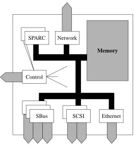
Fully compliant with the SPARC Compliance Definition (SCD); applications can be ported between SCD environments without change.Figure 1-1 Board Overview
Ethernet SPARC
SBus SCSI
Control
Memory
3
MK401 Board Description
2
Interconnection of the processing devices and the memory system is via the in-dustry standard SPARC MBus architecture using a 40MHz, level 2 cache coher-ent implemcoher-entation. Interfacing the MBus are two additional buses; the SBus connects the major I/O devices (such as the SCSI controllers), and the I/O bus connects minor I/O devices (such as the real time clock).
Running throughout the whole CS-2 system is a control network (CAN) used to distribute status and configuration information, to provide remote control and di-agnostics of all processors, and to create remote console connections to the proc-essors. The MK401 has two interfaces to this network; one connected to the I/O bus (and thus providing a direct interface to the SPARC processors) and one via a dedicated micro-controller which provides board control.
•
4 execution units offering parallel execution of major instruction types: Load/Store, Branch/Call, integer and floating point units.•
Dual instruction fetch per clock cycle.•
8Kbyte 2-way set-associative on-chip instruction cache.•
Instruction pipelining including a cache stage to accommodate the latency for second level cache accesses on data. Simultaneous accesses to on-chip and second level cache for each instruction fetch.•
High bandwidth 64bit Intra Module Bus (IMB) provides the interface between the CPU and the second level cache. Use of second level cache decouples the processor clock rate from the lower MBus clock rate.Key features of the RT625 (CMTU) and RT627 (CDU) devices are:
•
Full level 2 cache-coherent MBus compatibility.•
Each CDU has integral 16Kbytes x 32bit SRAM. MBus modules use either 2 or 4 CDUs for 128Kbyte or 256Kbyte second level direct-mapped cache.•
Physical cache tagging with virtual indexing allow the cache coherency logicto determine snoop hits and misses without stalling the CPU’s access to the cache.
•
Both copy-back and write-through cache modes supported.•
32 byte read buffer and 64 byte write buffer for buffering the 32 byte cache lines in and out of the second level cache.•
SPARC reference MMU offering 64 entry, fully set-associative TLB with 4096 contexts.Texas Instruments Viking Module
MK401 Board Description 9
2
Memory Configurations
The memory controller used by the MK401 offers a 128bit wide data bus for fast memory access, with single bit error correction, 2 bit error detection, and multi-ple bits within nibble detection. Memory errors are logged by kernel software and propagated via the CAN bus.
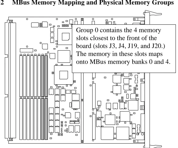
Up to 16 memory modules may be fitted to the MK401 offering a maximum of 512Mbytes. Both single and double sided, 4Mbit and 16Mbit SIMM may be used. The 16 sockets on the board are configured as 4 groups of 4 sockets; within each group the SIMMs must be identical, but there is no requirement for the groups to be the same.
Memory is mapped into the MBus address space in 8 banks of 64Mbytes. Bank 0 maps onto one side of the SIMMS in physical group 0. Bank 4 maps onto the second side of the SIMMS in physical bank 0. If less than 64Mbytes of memory is present in a bank it is echoed throughout the 64Mbytes. For each 128bit MBus data access 4 bytes are read from each SIMM.
Figure 2-2 MBus Memory Mapping and Physical Memory Groups
MK401 Board Description 11
2
•
A single CAN device provides both SPARCs with an interface to the machine-wide control area network (CAN). The SPARC processors write diagnostic information to this bus, and can also act as X-CAN or G-CAN routers. CAN routers transfer data between two levels of the CAN network; an X-CAN router handles transfers between the modules in a Cluster, and a G-CAN router handles transfers between Clusters. The configuration of a SPARC as a router will cause it’s CAN device to generate numerous level 2 interrupts which will impact on processor performance.Board Control Processor
13
Using the MK401
3
This chapter describes the usage of the MK401 in terms of its installation, hard-ware interfaces, and field serviceable components.
Installation
The MK401 is designed for use solely in a CS-2 Processor Module. The Proces-sor Module supplies the board’s power, cooling, and connection to the CS-2 data and control networks. The MK401 is fitted into one of the four vertical board slots behind the Processor Module’s removable front panel.
Warning – You must disconnect the power fr om the Processor Module be-fore removing or installing pr ocessor boards.
Warning – The board may be fitted with fragile or static sensitive devices. You must handle with car e and observe anti-static pr ecautions.
Removing the Module’s Front Panel
The module’s front panel is held in position by four clips, one in each corner. To remove the panel pull firmly away from the module.
Use the reverse procedure to install the LEDs and front panel.
Installing the Processor Board
Insert the board so that it fits into the guide rails at the top and bottom of the mod-ule’s board rack, ensuring that the component side is to the left (viewed facing the module). Gently push the board squarely on its front panel. Before pushing the board fully into position fold back the levers at each end of the front panel so that they are at 90o to the board; now push the board (while holding the levers) until the base of the two levers is touching the card cage. To lever the board into its final position push both levers until they lie flat on the board’s front panel. Se-cure the board by tightening the two captive screws.
Use the reverse procedure to remove the board.
Warning – You should take car e not to damage the connectors at the r ear of the board and on the module’ s backplane. Ensur e that the board mates squarely with the module’ s backplane.
Warning – When r emoving or installing a board you should take car e not to damage the RFI (copper) seals along the edge of the board’ s front panel.
Using the MK401 15
3
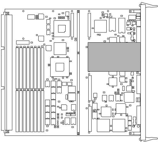
Field Serviceable Components
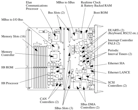
The MK401 has the following field serviceable components.
•
Superscalar SPARC processor modules fitted to MBus slots.•
Three SBus slots.•
16 memory slots.•
Boot ROM.•
H8 ROM.•
Realtime clock and non-volatile RAM (NVRAM).•
Fuses.The location of these components on the MK401 is shown in Figure 3-1.
Warning – User ’s are not permitted to make mechanical or electrical modi-fications to the equipment. Meiko is not r esponsible for r egulatory compli-ance of equipment that has been modified. Y ou will invalidate your warranty if you make unauthorised changes.
Figure 3-1 Field Serviceable Components
Elan
Bus Slots (2)
SBus Slots (3) Memory Slots (16)
Boot ROM Realtime Clock
H8 ROM
MBus (processor) and SBus (peripheral) plug-in modules are not shown.
& Battery Backed RAM Communications
Processor
Keyboard Fuse
Ethernet Fuse
Using the MK401 17
3
Installing MBus Processor Modules
Superscalar SPARC modules may be installed in the two MBus sockets — when using just one module it must be installed in position 0 (the slot nearest the com-munications processor and the rear of the board). The sockets are polarised to prevent incorrect installation.
Installation is simple — push the processor module into the connector on the MK401 and secure into position with an M3 screw at each corner.
Figure 3-2 Position of MBus Module 0
Installing SBus Modules
SBus devices are numbered from 0 to 2, device 0 being next to the processor slots. Device 4 is the board Ethernet and SCSI bus. Device 5 is the second on-board SCSI bus.
Figure 3-3 Position of SBus Module 0
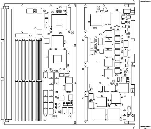
Memory
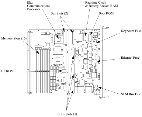
Up to 16 single in-line memory modules (SIMMs) may be fitted to the MK401 board (JEDEC 36 bit SIMMs). The array is constructed of 4 groups of 4 SIMMs, arranged as shown in Figure 3-4. Within each group the SIMMs must be identi-cal, but there is no requirement for the groups to be the same.
SIMMs can use either 4 Mbit DRAM or 16 Mbit DRAM technology, and be either single or double sided. This gives a minimum memory configuration of
Using the MK401 19
3
Figure 3-4 Memory slots on an MK401; the shaded region shows one of the 4 groups of 4 memory slots.
Boot ROM and H8 ROM
Both of these ROMs may be upgraded from time to time. They are held in sockets and are readily replaced. Note the position on pin 1 before removing the old de-vice (usually marked by a dot on the packaging).
Realtime Clock and Battery backed RAM
The real time clock and non-volatile RAM device is held in a DIL socket and is easily replaced. Before removing the old device note the position of pin 1 (usu-ally marked by a dot on the packaging). Note that the information within the RAM can only be restored by Meiko’s engineers.
Fuses
There are 3 fuses on the MK401:
Keyboard fuse: 20× 5mm 1 A quick blow ceramic. Ethernet fuse: 20× 5mm 1 A quick blow ceramic. SCSI bus fuse: 20× 5mm 500 mA quick blow ceramic.
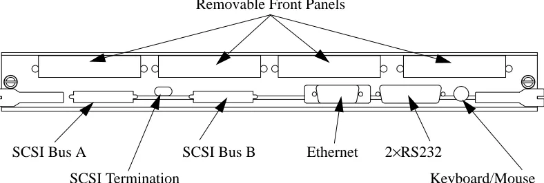
External Connections
External connections are provided for a keyboard/mouse (8 pin circular socket), serial interfaces (2 channels provided by one 25-way D-type connector), Ethernet (15-way D-type connector), and two independent SCSI buses (each via a 50-way miniature connector).
Front Panel Connections
Removable panels provide access to connectors on the optional SBus boards.
Figure 3-5 MK401 Front Panel Connections
Removable Front Panels
SCSI Bus A SCSI Bus B Ethernet 2×RS232
con-23
MBus Address Map
A
This section identifies the key devices used on the MK401 and lists their mapping into the MBus physical address space.
For detailed information about any of the devices you should refer to the manu-facturer’s data sheets.
The following notes are associated with the tables:
1. These locations are byte-wide and are mapped into all 4 bytes of a word. Care should be taken to generate correct byte-wide accesses to the least significant byte of the word in order to maintain future compatibility.
2. These locations are byte-wide memory, mapped into contiguous byte loca-tions. Word or halfword accesses will be automatically mapped into several successive byte-wide accesses.
3. These locations are byte sized registers which are only mapped into the most significant byte of a halfword. To ensure comparability with other boards only byte accesses at the correct address should be used.
SBus DMA chip A, Ethernet and SCSI
An Emulex FAS101 SCSI controller and an Advanced Micro Devices AM7990 Ethernet controller (LANCE) provide the MK401’s SCSI-A bus and Ethernet. The following table identifies the memory mapping for the SBus DMA device, the SCSI, and the Ethernet controllers.
e30800014 SCSI_B Interrupt R 2
e30800014 SCSI_B Select/Reselect Timeout W 2
e30800018 SCSI_B Sequence Step R 2
e30800018 SCSI_B Synchronous Period W 2
e3080001c SCSI_B FIFO Flags R 2
e3080001c SCSI_B Synchronous Offset W 2
e30800020 SCSI_B Configuration 1 RW 2
e30800024 SCSI_B Clock Conversion Factor W 2
e30800028 SCSI_B Test mode W 2
e3080002c SCSI_B Configuration 2 RW 2
e30800030 SCSI_B Configuration 3 RW 2
e30800034 SCSI_B Reserved
e30800038 SCSI_B Transfer Count High RW 2
e3080003c SCSI_B Reserved
e30800040 to e30bfffff
Unused (echoes of above)
e30c00000 to e3fffffff
Reserved (Read Undefined)
MBus Address Usage Read/
Write
MBus Address Map 29
A
Memory Controller
The MK401 uses an LSI Logic L64860 memory controller.
The following table shows the MBus memory maps for the memory controller’s control and diagnostic ports.
MBus Address Usage Read/
Write
Note
f00000000 Memory Enable RW
f00000004 Memory Delay RW
f00000008 Fault Status R(W)
f0000000c Video Config. RW
f00000010 Fault Address 0 R
f00000014 Fault Address 1 R
f00000018 ECC Diagnostics RW
f0000001c to f0fffffff
Unused (Read undefined)
f00000000 to fefffffff
39
NVRAM Variables
B
The battery-backed RAM in the realtime clock module is used to used to store basic machine start-up and communication options.
These parameters may be queried using the Forth Monitor (i.e. at theok prompt):
For example:
Alternatively the System Administrator can use theeeprom(1m) command to view and change the variables direct from a Unix command shell. For example:
Some of the parameters (those marked in the following list) may also be modified using the Set function in Pandora’s Network and Configuration Views.
printenv Display current variable settings.
setenv variable value Assign (or reassign) a value to a variable.
set-default variable Restore the variables default value.
set-defaults Restore the default values to all variables.
ok setenv output-device can
Variable Default Description
sbus-probe-list 43012 Identifies the SBus slots to probe and the probe order.
keyboard-click? false If true, enable keyboard click.
keymap no default Name of custom keymap file.
output-device
†
screen Power-on output device. One ofscreen,can,ttya, orttyb. Usecan to enable console connections to be grabbed bycancon(1m) and Pandora.
input-device
†
keyboard Power-on input device. One ofkeyboard,can,ttya, orttyb. Usecan to enable console connections to be grabbed bycancon(1m) and Pandora.
cancon-host 4294967295 Used to record the host of thecancon(1m) remote console connection through a reboot of this
processor. Do not change.
elanip-broadcast-high
†
4096 Highest Elan Id in network.elanip-broadcast-low
†
0 Lowest Elan Id in network.ep-btxpktlifetime
†
1000 Elan packet characteristics.ep-btxtimeout
†
1000 Elan packet characteristics.ep-txpktlifetime
†
10000 Elan packet characteristics.ep-txtimeout
†
10000 Elan packet characteristics.ep-bigmsgbcastboxes
†
4 Elan packet characteristics.ep-bigmsgboxes
†
32 Elan packet characteristics.ep-bigmsgsize
†
20416 Elan packet characteristics.ep-smallmsgbcastboxes
†
4 Elan packet characteristics.NVRAM Variables 43
B
†
These parameters may be changed using the Set function in Pandora’s Network and Configuration Views.security-#badlogins no default System set variable showing the number of times a bad password was specified.
oem-logo no default Byte array OEM logo (enabled byoem-logo?). Create a Forth array containing the logo and then copy into theoem-logo field.
oem-logo? false Enables OEM logo defined byoem-logo.
oem-banner no default Text displayed in the custom OEM banner alongside the OEM logo. Enabled byoem-banner?.
oem-banner? false Enables OEM banner text specified in oem-banner.
hardware-revision no default Hardware revision of this board (e.g. Rev D).
last-hardware-update no default Date of board’s manufacture or last upgrade (e.g. 25May94).
testarea 0 Unused.
mfg-switch? false If true, perform repeated self tests.
diag-switch? false Run in diagnostic mode.
45
Forth Monitor Commands
C
The following commands have been added to the Forth Monitor and are in tion to the commands that are normally present on a Solaris system. The addi-tional commands relate to the Control Network (CAN) and Elan network.
CAN Commands
To test and use the CAN bus you need to understand CAN addresses.
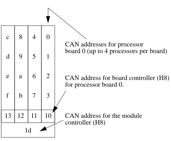
Nodes are addressed by their physical position in terms of Cluster, Module, and Node id’s (CMN). In CAN packets each of these id’s is represented by a 6bit field; the hexadecimal representation of these three 6bit fields is a Node Id. The module id is derived from the switch at the rear of the module. The number-ing of the nodes within a module is shown in Figure C-1.
Forth Monitor Commands 47
C
Testing the CAN Interface Device
Thetest command tests the SPARC’s CAN device by writing various values into its test register. The test is repeated using the test registers on the board con-troller’s H8 and the module concon-troller’s H8.
Testing the CAN Bus
You can test the CAN bus connection between nodes by using thertest com-mand. In the following example data is transferred from the current node to node 4:
ok test /can
Register test 0x00: OK Register test 0xff: OK Register test 0xaa: OK Register test 0x55: OK Checking on-board H8: OK.
Checking module controller: OK.
ok 4 rtest
Performing remote write/read test on node 4 Remote node type is MK405
Checking the Board and Module Controllers
You can check that both the board controller and module controller H8 proces-sors are running by using theping-h8 andping-module commands. Note that you need to change directory to/can before you use these commands.
Querying CAN Bus Usage
You can query the utilisation of the CAN bus by using theperf command. This command shows the number of CAN packets received since the machine was powered-up, and the number since the last query. You need to change to the
/can directory before using this command:
ok cd /can ok ping-h8
On-Board H8 is MK401. ok cd ..
ok cd /can ok ping-module
Module controller is MK515. ok cd ..
ok cd /can ok perf
Forth Monitor Commands 49
C
Monitoring CAN Bus Packets
You can snoop the CAN bus (monitor that packets on the bus) using thesnoop
command. Note that you cannot use this facility if you are connected to the Forth Monitor via a cancon connection. You need to change to thecan directory before using this command.
CAN Addresses
To determine the CAN address of this node use.can-id. This displays the node’s address in terms of its CMN, Node Id, and Slot Id. The Slot Id is for Meiko engineering use1.
Similarly the CAN address of the board’s controlling H8 processor can be ob-tained with the.h8-id command:
1. The slot id is the node’s physical position in the machine represented by a 5 bit cluster number, a 5 bit module number, a 2 bit slot number, 2 unused (always 0 bits), and a 2 bit processor number; the 2 bits that represent the slot number are transposed.
ok cd can ok snoop
Can’t can-snoop if you are a cancon slave ok cd ..
ok .can-id
SlotId: 0090, CAN Node-id: 00088 [00:02:08]
ok .h8-id
The CAN address of the H8 that controls the board’s module can be determined by the.module-id command:
You can convert from CAN node id’s to Cluster, Module, Node addresses (and vice versa) by using thecanid>cmn andcmn>canid commands respectively. Note that you need to change directory tocan before you use these commands.
Querying CAN Objects
Can packets include a 10 bit address space which, although not sufficient to map into the MBus/H8 physical address space, is adequate to map-in various status and control devices. These are referred to as CAN objects. Reading or writing to these objects allows you to query the status of a processor, board, or module, and to issue control instructions. See the header file /opt/MEIKOcs2/inclu-de/canio/canobj.h for a list of object addresses and their meanings. Local CAN objects are those that relate directly to this node. Remote CAN ob-jects maybe those of a board, module controller, or remote SPARC.
ok .module-id
The module controller is node 0009d.
ok cd can ok 4 canid>cmn 0 0 4
ok cd .. ok cd can
Forth Monitor Commands 51
C
You use therlo command to read a local object. You need to pass an object id on the Forth stack; in the following example we request the board type and are returned 191 (an MK401):
To read a remote object you need to push onto the Forth stack a CAN node id and the object id. In the following example we request the board type of nodec1
(module 3, board 0, node 2), which is an MK405:
The following additional example fetches the board type of nodedd, which is the controller for module 3, cluster 0:
Similar commands exist to write to CAN objects, but their direct use is not rec-ommended (they can reconfigure and reset the machine).
Remote Console Connections
You can create a console connection to a remote node by usingcancon. You need to pass on the Forth stack a CAN node id.
ok 0 rlo Read: 191
ok c1 0 rro Read: 195
You cannot create acancon connection from within an existing cancon connec-tion. If you are remotely interacting with a node’s Forth monitor viacancon (or Pandora) an attempt to create anothercancon connection will fail.
If your node is currently serving a remote console connection to someone else you can force it to disconnect that connection by usingcancon-dis. In the fol-lowing example the current connection to node 8 is dropped:
Elan Commands
The Elan device includes self test code that can be executed by thetest-all
command (which tests memory, SBus, CAN, Elan and all other devices with self test code) or explicitly by thetest /elan command.
ok 4 cancon
Connected to node 00004 cs2-4 console login:
ok 8 cancon-dis
Disconnecting node 00008 [00:00:08] ...
ok test /elan
Initialising Elan/Selftest software ... OK Checking threads processor ... OK
Testing from level 1 to level 1. Generating a route to level 1 ... OK Ping ... OK
Check-Ping ... OK
Spraying data to top switch ... OK Testing spray buffer ... OK