Iranian Journal of Electrical and Electronic Engineering, Vol. 16, No. 1, March 2020 1
A Coupled Inductor Based High Voltage Gain DC-DC
Converter Using Interleaved Voltage Multiplier Cells
S. Pourjafar*, H. Shayeghi*(C.A.), H. Madadi Kojabadi**, M. Maalandish***, and F. Sedaghati*
Abstract: In this work, a non-isolated high step up DC-DC converter using coupled inductor and voltage multiplier cell is proposed. The proposed converter conversion ratio is efficiently extended by using a coupled inductor. An interleaved configuration of two diode-capacitor cells is applied to step up the voltage conversion ratio and decrease the voltage stress across the switches. Also, in the suggested converter high voltage gain is provided by low turn ratio of the coupled inductor which decreases the volume of cores. Moreover, the reverse recovery problem of output diode is diminished by recycling the leakage inductance energy of the coupled inductor. It causes to increase the overall system efficiency. Furthermore, the voltage multiplier cells lead to clamp the voltage spikes through the switch, when the switch turns off. The comparison between the suggested converter and similar converters is provided to verify its advantages. To validate the effectiveness of the suggested converter, a 200W laboratory prototype with 20V input and 150V output voltages operating at 25kHz switching frequency is carried out and experimental test consequences are given.
Keywords: Non-Isolated Converter, High Conversion Ratio, Coupled Inductor, Voltage Multiplier Cell.
1 Introduction1
HOTOVOLTAIC (PV) is one of the best techniques for absorbing green energy to solve the serious problems of global warming and lack of energy that occurs by energy consumption [1-3]. Also, PV is one of the most significant systems for receiving energy in the world and it will have the largest share of electricity generation among all renewable energy candidates until 2040 [4]. But there are some drawbacks in terms of PV systems as follow [5, 6]:
Iranian Journal of Electrical and Electronic Engineering, 2020. Paper first received 14 April 2019, revised 02 November 2019, and accepted 06 November 2019.
* The authors are with the Electrical Engineering Department, University of Mohaghegh Ardabili, Ardabil, Iran.
E-mails: [email protected], [email protected], and
** The author is with the Faculty of Electrical and Computer Engineering, Sahand University of Technology, Tabriz, Iran. E-mail: [email protected].
*** The author is with the Faculty of Electrical and Computer Engineering, University of Tabriz, Tabriz, Iran.
E-mail: [email protected]. Corresponding Author: H. Shayeghi.
The magnitude of produced voltage by PV panels
is low and is changed by ambient temperature and solar radiation;
The capability of the used converter to track the maximum power point is complex;
The efficiency of PV modules is low.
Therefore, DC-DC converters with high conversion ratio are needed to convert the PV generated low voltage to the required high voltage level [7]. The conventional boost and buck-boost converters are famous topologies to step up the voltage. High voltage gain cannot obtain for these topologies due to losses caused by the inductor, filtering capacitor, switch and output diode. But then, the extreme increase in duty ratio of switch, makes the reverse recovery problem appear seriously and also, the power rating of the diode is increased [8-11]. The quadratic boost structure, which utilizes a single power switch, is another converter to step up the voltage, where the conversion ratio is specified as a quadratic function of the duty ratio [12, 13]. However, excessively increasing of duty cycle in these topologies restricts the switching frequency and system size. So, under this condition, the output voltage is very low and the problem of electromagnetic
P
Iranian Journal of Electrical and Electronic Engineering, Vol. 16, No. 1, March 2020 2
interference (EMI) is intensified [14]. However, a lot of active switches are necessary to realize a high voltage gain. Also, the control unit is complicated, which causes the complexity of the power circuit and also cost increasing [15]. A coupled inductor is modeled as a transformer function to increase the voltage conversion ratio in non-isolated DC-DC converters [16-19]. The main drawback in terms of these converters is voltage spikes through the active switches due to the leakage inductance and high costs. In order to solve these problems, the clamped circuits are utilized which can provide zero voltage operation of switches (ZVS) and zero current operation of switches (ZCS) conditions, which results in complexity of power circuit and its high cost [20-22]. Various high gain DC-DC structures based on the coupled inductor and switch capacitor structure have been introduced in the literature [23, 24]. The main features of these converters are that the voltage conversion ratio can be regulated in PWM mode; less active power switches and magnetic components are utilized. In order to achieve high voltage gain, the switched capacitor units and the boost converter can be combined [25-27]. These converters can obtain appropriate voltage gain with low current ripple contents which leads to reduce the EMI. The basic impediment of these topologies is high current and voltage ripples [27]. Interleaved converters with small size, weight and a small amount of magnetics are used in high power applications. Therefore, the sizes of input inductors and capacitors are intensely reduced. The voltage stress through the power switches is not higher than the half of the produced voltage for a single multiplier stage. However, reverse recovery currents through the multiplier diodes are large [28].
In this study, a novel non-isolated DC-DC converter with high conversion ratio is proposed. The suggested structure consists of a coupled inductor with two windings, just one active switch and two interleaved voltage multiplier units that are composed of diodes and capacitors. The voltage gain of the presented converter depends on the turn's ratio of the coupled inductor. The produced leakage inductance energy by coupled inductor is retrieved which leads to improving the overall efficiency of the converter. The diode-capacitor units are utilized to increase the output voltage and also, clamp the voltage through the switch which leads to reduce the voltage stress of the semiconductors. Thus, by using single switch with lower resistance RDS (on), the conduction losses are reduced.
2 Operational Function of Proposed DC-DC Converter
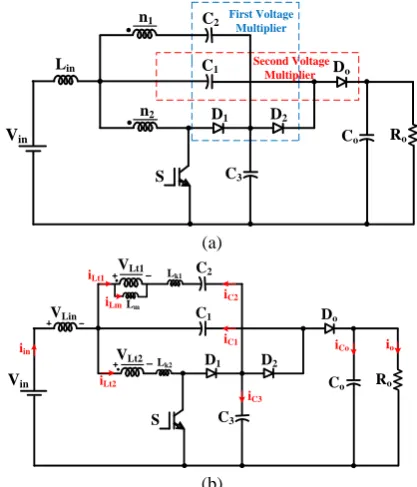
Fig. 1 illustrates the power circuit and equivalent circuit of the suggested topology. As shown in this figure, the proposed structure includes single active switch, an input inductor Lin for reduction of input
current ripple, a coupled inductor contains inductors Lt1
and Lt2 with n=2, the first voltage multiplier cell contains two capacitors C2 and C3, and diodes D1 and
D2, and second voltage multiplier cell contains capacitor
C1 and diode Do. Capacitor C3 and diode D1 act as a clamp circuit to decrease the peak voltage of the switch. The coupled inductor’s primary and secondary inductors are denoted via Lt1 and Lt2. An ideal transformer with turn ratio of n (n1/n2) is used for modeling the coupled inductor where Lk is leakage inductance and Lm is
magnetizing inductance.
To ease the analysis of the presented converter, the following suppositions are considered:
All capacitors have large contents as their voltages
are fixed during one switching period.
Input current (iLin) is continuous because of large
input inductance.
The used elements are ideal except the leakage
inductance of the coupled inductor.
The proposed converter operation in CCM
(Continuous Condition Mode) and DCM
(Discontinuous Conduction Mode) are analyzed as given in the following. In order to facilitate the analysis, the leakage inductor of the coupled inductor (Lk), is
ignored during the CCM and DCM operations.
2.1 CCM Operation
The basic waveforms of the converter operation in CCM are illustrated in Fig. 2(a). Two time intervals can be considered for each switching period in CCM operation.
First Mode: At this time instant, the switch S starts to conduct. Diodes D1 and Do are in reverse bias by
voltages VC3 and Vo-VC3, respectively. The only diode
n2
n1
C1
C2
C3
D1 D2
Do
Co Ro
Lin
Vin
S
First Voltage Multiplier
Second Voltage Multiplier
(a)
VLt1
Lm
VLin
iin V
Lt2
iLm
io
iC1
iC3
iC2
iCo
iLt2
iLt1
C1
C2
C3
D1 D2
Do
Co Ro
Vin
S
Lk1
Lk2
(b)
Fig. 1 Equivalent circuits of suggested converter: a) power circuit, and b) equivalent model.
Iranian Journal of Electrical and Electronic Engineering, Vol. 16, No. 1, March 2020 3 VGS
ILin
t
VDS
ILm
VD1
VD2
VDo
t
t
t
t
t
t DTs
(1-D)Ts VGS D
ILin
t
VDS
ILm
t
t
t DTs
ILt2
ID1
Ts
(a) (b)
Fig. 2 Basic waveforms of the suggested converter: a) CCM operation, and b) DCM operation.
D2 is conducting in this mode. DC energy from input source is transferred to the input inductor and the coupled inductor’s secondary side. It increases currents
iLin and iLt2 linearly and both inductances are charged. In this mode, capacitors C2 and C3 are discharged and
clamp through the voltage of capacitor C1 and
secondary side of the coupled inductor, Lt2. Therefore,
the capacitor C1 voltage can be increased by the stored
energy in the coupled inductor. The current track of the first mode is depicted in Fig. 3(a).
Second Mode: In this time instant, the power switch is switched off. At this time, diodes D1 and Do start to
conduct and diode D2 is blocked by voltage Vo-VC3. The stored energy in inductor Lin is transferred to the
magnetizing inductance of coupled inductor (Lm), and
input inductance is discharged. It increases current iLm
linearly. Also, the stored energy in inductor Lt2charges
capacitors C2 and C3. In this mode, the energy required for the load is provided from the input voltage Vin, input
inductor and the stored energy in capacitor C1 which increases the output voltage. The current track of this mode is depicted in Fig. 3(b).
2.2 DCM operation
Converter operation in DCM is divided in three switching modes. Fig. 2(b) illustrates the basic waveforms of voltage and current of the converter operation in DCM. Modes 1 and 2 are similar to modes 1 and 2 in CCM operations, which are depicted in Figs. 3(a) and 3(b), respectively. Mode 3 is occurred when the energy of the secondary side of the coupled inductor (Lt2), is completely depleted. In this time interval, the active switch is still OFF and diodes D1 and
D2 are reverse biased by voltages VC3-VSWand Vo-VC3,
respectively. Only diode Do conducts in this time
interval. During this switching time, the current which flows in the secondary side of the coupled inductor (iLt2), decrease to zero. The load required energy is provided from output capacitor Co, DC source, input
VLt1
Lm VLin
VLt2
io
iCo
iLt2
VC1
VC2
VD1 D2
VDo
VCo
Vin
S
Lk1
Lk2
VC3
Vo
(a) VLt1
Lm VLin
VLt2
iLt2
VC1
VC2
D1 VD2
Do
VCo Vin
S
Lk1
Lk2
VC3
Vo
(b) VLt1
Lm VLin
VLt2
iLt2
VC1
VC2
VD1 VD2
Do
VCo
Vin
S
Lk1
Lk2
VC3
Vo
(c)
Fig. 3 The current track of operation modes during switching time: a) switch is on, b) switch is off, and c) DCM operation.
inductor, and capacitor C1. Fig. 3(c) illustrates the current track of the third Mode in DCM operation.
3 Steady-State Analysis of Suggested Converter
This section provides the steady-state analysis of the suggested converter operation. In order to have a simple analysis, all converter elements are assumed to be ideal. In addition, the leakage inductance is ignored in analysis of the coupled inductor because of its small value. The converter operation is studied in all CCM, DCM, and BCM (Boundary Conduction Mode) conditions.
3.1 CCM Operation
Two different modes are considered for the converter operation in CCM. The equations related to Fig. 3(a), can be written as follows.
1 3
Lin in C C
V V V V (1) The voltages across inductors Lt1 and Lt2 are calculated as given in (2) and (3).
1 2 1
Lt C C
V V V (2)
2 3 1
Lt C C
V V V (3)
As shown in Fig. 3(b), the switch S is switched off in
Iranian Journal of Electrical and Electronic Engineering, Vol. 16, No. 1, March 2020 4
second mode and above equations can be rewritten.
1
Lin c in o
V V V V (4)
1 2 1 3
Lt o C C C
V V V V V (5)
2 1 3
Lt o C C
V V V V (6) Volt-second balance law is utilized for the inductors Lin,
Lt1, and Lt2 as follows:
1( ) 1( )
0 0
s s
s
DT T
Lt on DT Lt off
V dt V dt
(7)( ) ( )
0 0
s s
s
DT T
Lin on DT Lin off
V dt V dt
(8)2( ) 2( )
0 0
s s
s
DT T
Lt on DT Lt off
V dt V dt
(9)From (1)-(9), the voltages of the capacitors C1, C2, and
C3 can be obtained as follows:
2
1
( 1) (2 1)
1 2 1
o in
C O
V D V D n D
V V
D n
(10)
2
( 1)
1 2 1
C in o
D D n
V V V
D n
(11)
3
( 1)
1 2 1
in C o V n V V D n
(12)
The voltage gain in CCM operation (MCCM), is obtained
as follows:
2 1
( 1)(1 )
o CCM
in
V n
M
V n D
(13)
With regard to Fig. 3(a), the peak voltage of the main switch (VSw), is determined as follows:
3
1
2 1
SW C o
n
V V V
n
(14)
Also, the voltage across diodes (VD1, VD2, and VDo) are
calculated as follows:
1
1
2 1
D SW o
n
V V V
n (15) 2 2 1
D Do o
n
V V V
n
(16)
3.2 DCM Operation
There are three time intervals in DCM operation. Modes 1 and 2 in DCM are similar to the modes 1 and 2 in CCM. Fig. 3(c) illustrates the mode 3 in DCM
operation. In this mode, only diode Do conducts and so,
the following equations are derived:
1 1 2 3
Lt o C C C
V V V V V (17)
2 0
Lt
V (18)
1
Lin c in o
V V V V (19)
Volt-second law is used for the coupled inductors and the following equations are achieved:
( )
(1) (2) (3)
1 1 1
0 ( ) 0
s s s
s s
DT D D T T
Lt DT Lt D D T Lt
V dt V dt V dt
(20)( )
(1) (2) (3)
2 2 2
0 ( ) 0
s s s
s s
DT D D T T
Lt DT Lt D D T Lt
V dt V dt V dt
(21)( )
(1) (2) (3)
0 ( ) 0
s s s
s s
DT D D T T
Lin DT Lin D D T Lin
V dt V dt V dt
(22)Therefore, the voltage across the capacitors C1, C2, and
C3 can be determined in the following.
2
1
( )
( 1) ( 2 1)
o C
D nD D V V
D D D D n
(23)
2
( 1)
( 1) ( 2 1)
o C
D nD D V V
D D D D n
(24)
3
( 1) (2 1)
( 1) ( 2 1)
C o
D D D D
V V
D D D D n
(25)
D' and the voltage gain of the suggested converter
during this time interval are calculated as given in (26) and (27).
(1 )
( 2 1) ( 1)(1 )
in
in o
D D V D
V D n V n D
(26)
( 2 1) ( 1)
( 1)(1 )
o DCM
in
V D D n D D M
V D n D
(27)
The peak current value through the secondary side inductor of the coupled inductor (IL2), is equal to:
2
(1 )
(1 2 ) s Lt o D DT I V n L (28)
By knowing that in steady-state operation, the average currents through the capacitors are zero, the average current of diodes D1, D2, and Do are equal to the average
of output current (Io), so we have:
1 2 2
1 2
D D Do o L
I I I I D I (29)
Substituting (28) and (29) into (26), the voltage conversion ratio of the converter in DCM is achieved as follows:
2 1
( 1)(1 ) 1 2 (2 1)
DCM
crit
D n D D
M
n D n k n
(30)
3.3 BCM Operation
Since the voltage conversion ratio in CCM operation is equal to the voltage gain in DCM operation, it means that the converter operates in BCM. Based on (13) and (27), the normalized time constant of boundary operation is represented by the following equations.
Iranian Journal of Electrical and Electronic Engineering, Vol. 16, No. 1, March 2020 5
CCM DCM
M M (31)
2
2( )
(1 )
2(2 1)
L crit
D D
n
(32)
Fig. 4 illustrates the curve of boundary normalized secondary winding of the coupled inductor time constant τL2(cirt) versus duty ratio (D). The suggested converter operates in the CCM when τL2(cirt) is higher than τL2. Conversely, the converter operates in DCM when τL2 is determined to be higher than τL2(cirt).
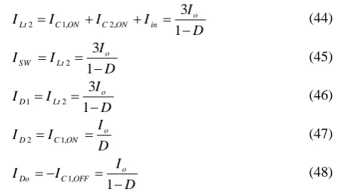
3.4 Current Analysis
In the first time interval, when the active switch is switched on, the capacitor currents are represented as follows:
1( ) 1 2
C ON Lt Lt in
I I I I (33)
2( ) 1
C ON Lt
I I (34)
3( ) 1( ) 2( )
C ON C ON C ON
I I I (35)
( )
CO ON O
I I (36)
When the switch is turned off in the second time interval, the following equations are achieved for the capacitors current:
1( ) 1 2
C OFF Lt Lt in
I I I I (37)
2( ) 1
C OFF Lt
I I (38)
3( ) 1 2( )
C OFF D C OFF
I I I (39)
( ) 1( )
CO OFF C OFF o
I I I (40)
By utilizing the current-second balance law for capacitors, the average current through the capacitors in the first and the second modes are achieved in the following:
1, 2, 3,
out
C ON C ON C ON
I
I I I
D
(41)
2, 1, 3,
1 out
C OFF C OFF C OFF
I
I I I
D
(42)
Now, by remarking n=2, the following equations are
obtained:
1 2,
o
Lt C ON
I I I
D
(43)
Fig. 4 Normalized inductor time constant of boundary operation.
2 1, 2,
3 1
o
Lt C ON C ON in
I
I I I I
D
(44)
2
3 1
o
SW Lt
I I I
D
(45)
1 2
3 1
o
D Lt
I I I
D
(46)
2 1,
o
D C ON
I I I
D
(47)
1,
1 o
Do C OFF
I I I
D
(48)
4 Key Parameters Design Procedure 4.1 Input Inductor
The converter input current ripple should be low as possible as, to increase the lifespan of energy sources connected to the converter. Therefore, input inductor (Lin) is designed to have an input current ripple value
nearly 10-20% of the average input current, which can be obtained as given in (49).
(2 1)
in in
s Lin
nV D L
n f I
(49)
4.2 Magnetizing Inductor and Turn Ratio of Coupled Inductor
Coupling inductive value is determined by magnetic
inductance (Lm). It is important to design the
magnetizing inductance as the converter works in CCM. So, the acceptable magnetizing inductor value is obtained as given in the following:
in m
s Lm
nV D L
f I
(50)
where ΔILm is the current ripple of the magnetizing
inductor. The turn ratio should be selected in such a way that the voltage rating of devices be low. To obtain the turn ratio of the coupled inductor, the following equation is used:
1
2
(1 )
(1 ) 2
o in
o in
V D V n
n
n V D V
(51)
The turn ratio of the coupled inductor is estimating by selecting the switching duty ratio, and also the power device voltage and current stresses can be determined.
4.3 Capacitors
The capacity of the output capacitor, Co, which limits
the output voltage in CCM operation, can be written as follows:
o o
s o o
P D C
f V V
(52)
Iranian Journal of Electrical and Electronic Engineering, Vol. 16, No. 1, March 2020 6
According to the capacitor currents, the capacity of the capacitors C1, C2, and C3is given as follows:
1,2,3
1,2,3 o
s o C
P C
f V V
(53)
ΔV is named as capacitor voltage ripple which is
considered 5-10% of average voltage. The voltage and current waveform of capacitors are depicted in Fig. 5.
4.4 System Losses Analysis
The power losses of the suggested converter can be divided into the following groups:
1. Power losses of the switch;
2. Power losses of the diodes;
3. Power losses of the Capacitors;
4. Power losses of the magnetic components.
Some variable symbols of parasitic elements are introduced in the following.
rDS-ON: resistance of power switch in On-state;
rC: ESR values of Capacitors;
rD: On-state resistance of diodes Do, D1, D2;
vFD: Diodes forward voltages;
rL: The ESR value of the magnetic components.
The power losses of the power switch can be determined by summation of the conduction and switching losses. The conduction loss of the active switch, PrDS, is achieved in the following.
2 ,
rDS DS S rms
P r I (54)
Switching loss is occurs when the active switch is switched ON and OFF. So, the converter switching loss (PSW), is written as follows:
1
( )
2
SW s r d sw sw
P f t t I V (55)
where fs is switching frequency, Vsw is the average
voltage through the switch, Isw is the average current
through the switch, tr is the rise time of the switch and td
is the turn-off delay time. Therefore, the total power loss of the switch (Pswitch) is obtained as given in (56).
switch rDS SW
P P P (56)
The major loss of a diode is conduction loss due to the existence of the internal resistance, and diode forwards voltage loss. The conduction losses through the Diodes are computed as follows:
2 ,
rf Diodes rms Diodes
P r I (57)
and diodes forward voltage losses are obtained as follows:
( Diodes) ( ) ( )
vF D F Diodes avg Diodes
P V I (58)
Power losses of capacitors due to ESR are determined as given in (58).
2
( ) ,
rC Capacitors Capacitors Capacitors rms
P r I (59)
The magnetic losses due to the existence of the coupled inductor and input inductor, are calculated in the following.
2 ,
rL L L rms
P r I (60)
By highlighting the overall system losses, the following equation is utilized to estimate the efficiency of the suggested converter:
100% out
out Loss
P P P
(61)
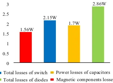
All mentioned losses by considering n=2, D=0.6 and
related to the experimental results in the nominal output power, are shown in Fig. 6. It should be noted that the core losses through the input inductor and coupled inductor are negligible by comparing to other conduction losses. Thus, in the efficiency calculation, the core losses are not considered.
4.5 Dynamic Response Analysis
The dynamic proficiency of the proposed structure is studied using the state-space average method. The system equations are provided as state, input and control
IC1
t
t DTs (1-D)Ts
VC1
ΔVC1
IC3
t
t DTs (1-D)Ts
VC3
ΔVC3
IC2
t
t DTs (1-D)Ts
VC2
ΔVC2
ICo
t
t DTs (1-D)Ts
VCo
ΔVCo
(a)
(b)
(c)
(d)
Fig. 5 Voltage and current waveforms of capacitors: a) C1,
b) C2, c) C3, and d) Co.
2.86W
0 0.5 1 1.5 2 2.5 3
Power losses of capacitors Magnetic components losses Total losses of switch
Total losses of diodes
1.56W
2.15W
1.7W
Fig. 6 Components power losses at full load.
Iranian Journal of Electrical and Electronic Engineering, Vol. 16, No. 1, March 2020 7
variable functions which are shown in the state-space form as follows.
ˆ ( ) ˆ ( ) ˆ( )
ˆ ( ) ˆ ( ) ˆ ( )
i i i
i i i
x t A x t Bu t
y t Cx t Du t
(62)
The following presumptions are investigated in order to have a state equation,
All components are considered ideal;
The input current is continuous.
In the analysis, ˆ ( )x ti is the vector of state variables,
ˆ ( )i
u t is the vector of input variables, and ˆ ( )y ti is the
vector of output variables which are defined as follow:
1 2 1 2 3
ˆ ˆ ˆ
ˆ [ Lin, Lk , Lk ,ˆC ,ˆC ,ˆC ,ˆCo]
x i i i v v v v (63)
1
ˆ ˆ ˆ
ˆ [ˆin, ,o D , ]
uv i i d (64)
ˆ ˆ [ in,ˆo]
y i v (65)
By utilizing Kirchhoff’s voltage and current laws for each mode of operations, the associated matrixes related to equation (62), is obtained:
1 1 1 1
2 2 2
1 1 1
2
3 3 3
1 1
0 0 0 0
1 1 1 1
0 0 0
1 2 1 1
0 0 0 0
1 1 1
0 0 0 0
0 0 0 0 0 0
1 2 1 3 1 2
0 0 0 0
1
0 0 0 0 0 0
in in in
k k k k
K K K
o
D D
L L L
D D
L L L L
D D
L L L
A
C C C
D C
D D D
C C C
D C (66) 3 3 1 3 2 1 2
1 2 1
3 3
1
0 0
0 0 0
2 0 0 0
0 0 0 0
0 0 0
3 1 0 0
1
0 0 0
o C in in C o k C o k Lk
Lk Lk Lin D
o V V L L V V L V V L B I C
I I I I
D C C C (67)
1 0 0 0 0 0 0
0 0 0 0 0 0 1
C
(68)
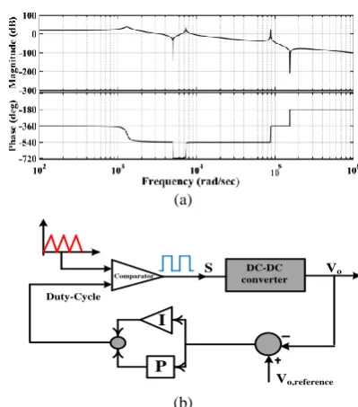
The dynamic analysis of the proposed converter based on open-loop transfer function has been performed using the Bode diagram. The element values are
determined as follows: Lk1=Lk2=2μH, Lin=1.5mH,
C1=C2=C3=200µF, Co=1500µF, D=0.6 and n=2. The
Bode diagram of the open-loop transfer function in the Laplace domain is depicted in Fig. 7. Regarding Fig. 7(a), the control loop can be designed for the suggested converter as depicted in Fig. 7(b).
5 Comparison Study
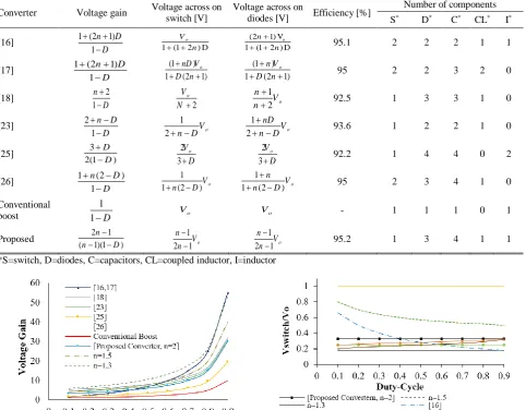
In this portion, the proposed DC-DC converter is compared with some similar topologies. Comparison results are given in Table 1.
By considering the voltage gain item, it is clear that
when the value of n is closer to 1, it leads to achieving
the higher voltage gain. In addition, it causes to reduce the normalized voltage stress through the power
components. Conventionally, n has to be large to
achieve a high conversion ratio, however, by increasing the value of n excessively, converter volume and cost will be increased. By considering the voltage gain equation of the suggested converter, it is clear that the high voltage conversion ratio is achieved for low value of n which leads to decrease in the core volume. Also, the efficiency of the proposed structure is compared with the other works at the same power.
Fig. 8(a) illustrates the voltage gain versus duty ratio for the proposed topology and the other converters. In this comparison, the coupled inductor turn ratio in all of the converters is equal to 2. The presented converters in [16] and [17] have high voltage rate, but they require an additional high rating switch which increases the cost of the converter. The converter proposed in [18] has high output voltage and high voltage stress through the switch. Also, the efficiency of the converter presented in [18] is too low for high voltage gain applications. Although, the structure introduced in [26] has a higher voltage gain in large duty cycles, but the peak voltage
(a) DC-DC converter Comparator S Vo,reference Vo Duty-Cycle P I (b)
Fig. 7 a) Open-loop transfer function of the suggested structure, and b) Control loop of the suggested structure.
Iranian Journal of Electrical and Electronic Engineering, Vol. 16, No. 1, March 2020 8
through the switch increases exponentially.
Related to the presented converter voltage gain equation, it can be noticed that by choosing the suitable turn ratio for the coupled inductor, a high voltage gain can be provided. Fig. 8(b) illustrates comparison results of the voltage stress through the active switch between the proposed structure and the other topologies. As shown in this figure, the voltage across the switch of the suggested converter is reduced when n > 1 and it is nearly equal to 1. Also, it can be concluded that the peak voltage of switch in the proposed topology is reduced by decreasing the turn ratio (turn ratio should be larger than 1). Indeed, the voltage gain and the peak voltage through the switch in the suggested converter have been improved by comparing the other converters.
Therefore, RDS-ON is decreased for the proposed
converter and also, the efficiency is increased. By considering the comparison results, it has to be
mentioned that the presented converter is a better choice for renewable energy systems.
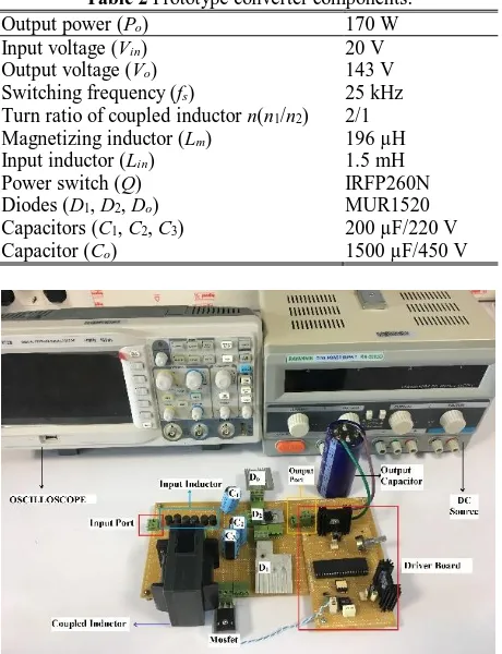
6 Experimental Test Result
For investigating the theoretical analysis, the topology of the suggested converter has been constructed and
tested in the laboratory. For the practical
implementation of the converter, a microcontroller is required to control and generate the switching signals. In this work, microcontroller ATMEGA16 has been used. The experimental prototype is shown in Fig. 9 which contains power circuit and control unit. The characteristic of the prototype components is shown in Table 2.
The basic experimental results waveforms of the converter operation in CCM are illustrated in Figs. 10-12. The voltage stress and gate driving waveforms of
Table 1 Comparison results of the proposed DC-DC converter with some of the previous converters.
Converter Voltage gain Voltage across on switch [V]
Voltage across on
diodes [V] Efficiency [%]
Number of components
S* D* C* CL* I*
[16] 1 (2 1)
1
n D
D
1 (1 2 ) D
o V
n
(2 1) V 1 (1 2 ) D
o n
n
95.1 2 2 2 1 1
[17] 1 (2 1)
1
n D
D
(1 ) 1 (2 1)
o
nD V D n
(1 ) 1 (2 1)
o
n V D n
95 2 2 3 2 0
[18] 2
1 n
D
2
o
V N
1 2 o n
V n
92.5 1 3 3 1 0
[23] 2
1 n D
D
1 2 n DVo
1
2 o
nD V
n D
93.6 1 2 2 1 0
[25] 3
2(1 )
D D
2 3
o
V D
2 3
o
V D
92.2 1 4 4 0 2
[26] 1 (2 )
1
n D
D
1 1n(2D)Vo
1 1 (2 ) o
n V n D
95 2 3 4 1 0
Conventional boost
1
1D Vo Vo - 1 1 1 0 1
Proposed 2 1
( 1)(1 )
n n D
1 2 1 o
n V n
1 2 1 o
n V n
95.2 1 3 4 1 1
*S=switch, D=diodes, C=capacitors, CL=coupled inductor, I=inductor
(a) (b)
Fig. 1 Comparison results of the presented converter and some similar structures: a) voltage gain in CCM operation, and b) voltage stress through the switch.
Iranian Journal of Electrical and Electronic Engineering, Vol. 16, No. 1, March 2020 9
the power switch are given in Figs. 10(a) and 10(b), respectively. As depicted in Fig. 10(b), the peak voltage through the main switch is about 49V which is too less than the output voltage. This advantage of the proposed converter allows utilizing a switch with low RDS-ON to
reduce the conduction loss. The input current waveform is shown in Fig. 11(a). It is obvious that the ripple of the input current is close to 0.6A and the percent of current ripple is about 6%. It is clear that the input current is continuous. The voltage waveforms of the high power diodes D1, D2, and Do are illustrated in Figs. 11(b)-(d),
respectively. The peak voltage through diode D1 is
about 49V which is shown in Fig. 11(b). The maximum
voltage across diode D2 is approximately 94V which is
shown in Fig. 11(c). Also, the voltage stress of diode Do
is about 94V which is illustrated in Fig. 11(d). It is clear that the voltage stress of the diodes is less than that of the other converters which leads to reduce conduction loss. The output voltage waveform and the measured voltage through the capacitors are illustrated in Figs. 12(a)-(d), respectively. Fig 12(a) shows the voltage waveform of the capacitor C1 which is about
66V. The voltage waveform of the capacitor C2 is given
in Fig. 12(b) which is approximately equal to 29V. As depicted in Fig. 12(c), the voltage through the capacitor
C3 is about 49V. The input voltage is 20V, as shown in
Fig. 12(d), the output voltage is boosted to almost145V. It has to be mentioned that the output voltage ripple is low and close to zero.
Table 2 Prototype converter components.
Output power (Po) 170 W
Input voltage (Vin) 20 V
Output voltage (Vo) 143 V
Switching frequency (fs) 25 kHz Turn ratio of coupled inductor n(n1/n2) 2/1
Magnetizing inductor (Lm) 196 µH
Input inductor (Lin) 1.5 mH
Power switch (Q) IRFP260N
Diodes (D1, D2, Do) MUR1520 Capacitors (C1, C2, C3) 200 µF/220 V
Capacitor (Co) 1500 µF/450 V
Fig. 9 Experimental prototype of the presented converter.
Theoretical analysis and experimental measurement results confirm that the suggested converter would be an appropriate choice for renewable energy systems such as PV due to its low input current ripple and high voltage gain. Because of the less number of power switch, lower peak voltage through semiconductors and the higher output voltage, the presented converter can be used for various power levels.
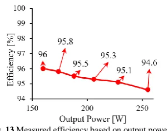
Converter measured efficiency based on output power is illustrated in Fig. 13. The used parameters in calculating the efficiency are n=2, D=0.6, fs=25kHz.
The maximum efficiency of the suggested structure is about 96% in output power of 150W. The measured efficiency for the proposed topology is almost 95.5% at full load operation (input source is 20V and produced power is 170W). According to Fig. 13, it is clear that tolerance at the measured power level is not high in the presented converter. When the output power changes between 150W and 250W, the efficiency tolerance is about 1.4%. By increasing the diode-capacitor unit, the produced voltage and current levels are increased,
(a) (b)
Fig. 10 Experimental measurement result of a) VGate, and b) VDS.
(a) (b)
(c) (d)
Fig. 11 Experimental measurement result of input current and voltage of diodes: a) iin, b) VD1, c) VD2, and d) VDo.
(a) (b)
(c) (d)
Fig. 12 Experimental measurement results of capacitors voltage: a)VC1, b) VC2, c) VC3, and d) VCo=Vo.
Iranian Journal of Electrical and Electronic Engineering, Vol. 16, No. 1, March 2020 10 Fig. 13 Measured efficiency based on output powers.
therefore, the produced power level will be increased. It leads to improve the efficiency of the suggested converter for a similar power range.
7 Conclusion
In this study, a novel non-isolated high step-up boost DC-DC converter using a coupled inductor was proposed. The voltage conversion ratio of the presented converter is increased by adjusting the turn ratio of the coupled inductor. The main merits of the suggested converter consist of decreasing the number of cores (with integrated coupled inductor), achieve to high voltage gain with lower turn ratio, decreasing the peak voltage through the power switch by adjusting the turn ratio, and get a high efficiency (about 95.5% at 170W). The mathematical and experimental results verify each other and also, indicate that the proposed structure is a suitable as an interface converter for renewable applications like PV panels.
References
[1] M. Maalandish, S. H. Hosseini, T. Jalilzadeh, and
S. Pourjafar, “A buck-boost DC/DC converter with high efficiency suitable for renewable energies,”
International Journal of Emerging Electric Power System, Vol. 19, No. 4, 2018.
[2] E. Babaei and Z. Saadatizadeh, “High voltage gain
DC–DC converters based on coupled inductors,”
IET Power Electronics, Vol. 11, No. 3, pp. 434–52, 2017.
[3] M. Maalandish, S. H. Hosseini, and T. Jalilzadeh,
“High step-up DC-DC converter using switch-capacitor techniques and lower losses for renewable
energy applications,” IET Power Electronics,
Vol. 11, No. 10, pp. 1718–1729, 2018.
[4] B. S. Revathi and P. Mahalingam, “Non-isolated
high gain DC–DC converter with low device stress and input current ripple,” IET Power Electronics, Vol. 11, No. 15, pp. 2553–2562, 2018.
[5] M. Maalandish, S. Pourjafar, S. H. Hosseini, and K. Taghizadegan, “Leakage current elimination with improved non-isolated nine-level inverter for
grid-connected PV panels,” Journal of Energy
Management and Technology, Vol. 1, No. 2, pp. 46-55. 2017.
[6] T B. Akhlaghi, N. Molavi, M. Fekri, and
H. Farzanehfard, “High step-up interleaved ZVT converter with low voltage stress and automatic
current sharing,” IEEE Transaction on Industrial
Electronics, Vol. 65, No. 1, pp. 291–299, 2018.
[7] P. Thounthong, B. Davat, S. Rael, and P Sethakul,
“Fuel cell high-power applications,” IEEE Industry
Electronic Magazaine, Vol. 3, No. 1, pp. 32–46, 2009.
[8] M. Maalandish, S. H Hosseini, S. Ghasemzadeh,
E. Babaei, R. S. Alishah, and T. Jalilzadeh, “Six-phase interleaved boost DC-DC converter with
high-voltage gain and reduced high-voltage stress,” IET Power
Electroics, Vol. 10, No. 14, pp. 1904–1914, Jul. 2017.
[9] F. M. Shahir, E. Babaei, and M. Farsadi, “A new structure for non-isolated boost DC–DC converter,”
Journal of Circuits, Systems and Computers; Vol. 26, No. 10, pp. 1750012, Jan. 2017.
[10]M. Maalandish, S. H. Hosseini, T. Jalilzadeh, and N. Vosoughi, “High step-up DC–DC converter using one switch and lower losses for photovoltaic
applications,” IET Power Electronics, Vol. 11,
No. 13, pp. 2081–2092, 2018.
[11]J. Leyva-Ramos, M. G. Ortiz-Lopez, L. H.
Diaz-Saldierna, and J. A. Morales-Saldana, “Switching regulator using a quadratic boost converter for wide
DC conversion ratios,” IET Power Electronics,
Vol. 2, No. 5, pp. 605–613, 2009.
[12]P. Saadat and K. Abbaszadeh, “A single-switch
high step-up DC–DC converter based on quadratic
boost,” IEEE Transaction on Industrial Electronics,
Vol. 63, No. 12, pp. 7733–7742, 2016.
[13]L. H. Barreto, E. A. Coelho, V. J. Farias,
L. C. de Freitas, and J. B. Vieira, “An optimal lossless commutation quadratic PWM boost
converter,” in Seventeenth Annual IEEE Applied
Power Electronics Conference and Exposition (Cat. No. 02CH37335), Vol. 2, pp. 624–629, 2002.
[14]J. Leyva-Ramos, R. Mota-Varona, M. G.
Ortiz-Lopez, L. H. Diaz-Saldierna, and D. Langarica-Cordoba, “Control strategy of a quadratic boost converter with voltage multiplier cell for
high-voltage gain,” IEEE Journal of Emerging and
Selected Topics in Power Electronics, Vol. 5, No. 4, pp. 1761–1770, 2017.
Iranian Journal of Electrical and Electronic Engineering, Vol. 16, No. 1, March 2020 11
[15]Y. Tang, T. Wang, and Y. He “A
switched-capacitor-based active-network converter with high
voltage gain,” IEEE Transactions on Power
Electronics, Vol. 29, No. 6, pp. 2959–2968, 2014. [16]H. C. Liu and F. Li, “Novel high step-up DC–DC
converter with an active coupled-inductor network
for a sustainable energy system,” IEEE Transactions
on Power Electronics, Vol. 30, No. 12, pp. 6476– 6482, 2015.
[17]Y. Tang, D. Fu, T. Wang, and Z. Xu “Analysis of
active-network converter with coupled inductors,”
IEEE Transactions on Power Electronics. Vol. 30, No. 9, pp. 4874–7882, 2015.
[18]M. Muhammad, M. Armstrong, and M. A Elgendy,
“Analysis and implementation of high-gain
non-isolated DC–DC boost converter,” IET Power
Electronics, Vol. 10, No. 11, pp. 1241–1249, 2017.
[19]M. Eskandarpour Azizkandi, F. Sedaghati, and
H. Shayeghi, “An interleaved configuration of modified ky converter with high conversion ratio for renewable energy applications; design, analysis and
implementation,” Journal of Operation and
Automation in Power Engineering, Vol. 7, No. 1, pp. 90–106, 2019.
[20]A. Ajami, H. Ardi, and A. Farakhor, “A novel high
step-up DC/DC converter based on integrating coupled inductor and switched-capacitor techniques
for renewable energy applications,” IEEE
Transactions on Power Electronics, Vol. 30, No. 8, pp. 4255–4263, 2015.
[21]F. Sedaghati, S. H. Hosseini, M. Sabahi, and G. B.
Gharepetian, “Analysis and Implementation of a
modular isolated zero-voltage switching
bidirectional DC–DC converter,” IET Power
Electronics, Vol. 7, No. 8, pp. 2035–2049, 2014.
[22]F. Sedaghati, S. H. Hosseini, M. Sabahi, and
G. B. Gharepetian, “Extended configuration of dual active bridge DC–DC converter with reduced
number of switches,” IET Power Electronics, Vol. 8,
No. 3, pp. 401–416, 2015.
[23]S. M. Chen, M. L. Lao, Y. H. Hsieh, T. J. Liang, and K. H. Chen, “A novel switched-coupled-inductor DC–DC step-up converter and its
derivatives,” IEEE Transaction on Industry
Application, Vol. 51, No. 1, pp. 309–314, 2015.
[24]Y. P. Hsieh, J. F. Chen, T. J. Liang, and L. S. Yang,
“Novel high step-up DC–DC converter with
coupled-inductor and switched capacitor
techniques,” IEEE Transaction on Industrial
Electronics, Vol. 59, No. 2, pp. 998–1007, 2012.
[25]S. Saravanan and N. R. Babu, “Design and
development of single switch high step-up DC-DC
converter,” IEEE Journal of Emerging and Selected
Topics in Power Electronics, Vol. 6, No. 2, pp. 855– 863, 2018.
[26]S. Sathyan, H. M. Suryawanshi, M. S. Ballal, and A. B. Shitole, “Soft-switching DC–DC converter for distributed energy sources with high step-up voltage
capability,” IEEE Transaction on Industrial
Electronics, Vol. 62, No. 11, pp. 7039–7050, 2015.
[27]B. Zhu, L. Ran, and X. Wu, “Kind of high step-up
DC-DC converter using a novel voltage multiplier
cell,” IET Power Electronics, Vol. 10, No. 1,
pp. 129–133, 2017.
[28]M. Khalilzadeh, B. Asaei, and M. R. Nikzad, “A novel interleaved DC-DC converter with reduced
loss for fuel cell vehicle application,” Iranian
Journal of Electrical and Electronic Engineering, Vol. 13, No. 1, pp. 89–99, 2017.
S. Pourjafar was born in May 1993 in Ardabil, Iran. He received his B.Sc. degree in Electrical Engineering from Azerbaijan Shahid Madani University, Tabriz, Iran, in 2015. He also received his M.Sc. at Power Electronics and Drives from Sahand University of Technology, Faculty of Electrical and Computer Engineering, Tabriz, in 2017. He is currently Ph.D. Candidate in Electrical Engineering Department, University of Mohaghegh Ardabili. His research interests include DC-DC converters, inverters, application of power electronics in energy conversion systems (wind energy, solar energy, grid connected inverters), battery charging application in electric vehicles.
H. Shayeghi received the B.Sc. and M.S.E. Degrees in Electrical and Control Engineering in 1996 and 1998, respectively, and the Ph.D. degree in Electrical Engineering from Iran University of Science and Technology, Tehran, Iran, in 2006. Currently, he is a Full Professor in the Technical Engineering Department of the University of Mohaghegh Ardabili, Ardabil, Iran. His research interests are in the application of robust control, artificial intelligence and heuristic optimization methods to power system control design, operation, and planning, power system restructuring, and renewable energies applications. He has authored and co-authored five books in the electrical engineering area, all in Farsi, one book and two book chapters in international publishers, and more than 320 papers in international journals and conference proceedings. Prof. Shayeghi collaborates with several international journals as reviewer board member and works on the editorial committee of eight international journals. He has served on several other committees and panels in governmental, industrial, and technical conferences. He was selected distinguished researcher of the University of Mohaghegh Ardabili several times. In 2007, 2010, 2011, 2013,
Iranian Journal of Electrical and Electronic Engineering, Vol. 16, No. 1, March 2020 12 and 2017 he was also elected as distinguished researcher in
engineering field in Ardabil province of Iran. He has been included in the Thomson Reuters' list of the top one percent of most-cited technical engineering scientists in 2015, 2016, 2017, and 2018, respectively. Also, he is a member of the Iranian Association of Electrical and Electronic Engineers (IAEEE).
H. Madadi Kojabadi (M’15) received the Ph.D. degree in Electrical Engineering from the University of New Brunswick, Fredericton, N.B., Canada in 2003. Since 1993, he has been a Faculty Member at Sahand University of Technology, Tabriz, Iran. During 2003-2004 he was Post-Doctoral Fellow at the University of New Brunswick, Fredericton, N.B., Canada. He has published over 100 papers in technical journals and conference proceedings and three books. He is currently a Professor and managing director of the Renewable Energy Research Center at SUT. His main research interests include renewable energy conversion, power electronic converters and variable-speed drives.
M. Maalandish was born in September 1990 in Marand (Yamchi), Iran. He received the B.Sc. degree in Electrical Engineering from Azarbaijan Shahid Madani University, Tabriz, Iran, in 2013 and the M.Sc. degree in Power Electronics in 2016 from Faculty of Electrical and Computer Engineering, Power Engineering Department, University of Tabriz, Tabriz, Iran, where he is currently working toward the Ph.D. degree. He is the author of more than 20 journal and conference papers. His research interests include power conversion (DC–DC and DC–AC), designing and controlling of power electronic converters, multi-input multioutput (MIMO) converters, MPC method, leakage current elimination, and renewable energies.
F. Sedaghati was born in Ardabil, Iran, in 1984. He received the M.Sc. and Ph.D. Degrees both in Electrical Engineering in 2010 and 2014 from the University of Tabriz, Tabriz, Iran. In 2014, he joined the Faculty of Engineering, Mohaghegh Ardabili, where he has been an Assistant Professor since 2014. His current research interests include renewable energies and power electronic converters design and applications.
© 2020 by the authors. Licensee IUST, Tehran, Iran. This article is an open access article distributed under the terms and conditions of the Creative Commons Attribution-NonCommercial 4.0 International (CC BY-NC 4.0) license (https://creativecommons.org/licenses/by-nc/4.0/).