EEMCS / Electrical Engineering
Control Engineering
On FPGAs with embedded processor cores
for application in robotics
Roderick Colenbrander
MSc report
Supervisors:
prof.dr.ir. J. van Amerongen dr.ir. J.F. Broenink ir. M.M. Bezemer ir. E. Molenkamp
August 2009
Glossary
ACE - Advanced Configuration Environment APU - Auxiliary Processor Unit
BIT - FPGA bitstream programming file BSP - Board Support Package
CE - Control Engineering CW - Configware
EDK - Platform Studio Embedded Development Kit ELF - Executable and Linkable Format
FPGA - Field Programmable Gate Array HDL - Hardware Description Language LVDS - Low Voltage Differential Signalling LUT - Lookup Table
MHS - Microprocessor Hardware Specification PLB - Processor Local Bus
SysACE - System Advanced Configuration Environment SysGen - System Generator for DSP
UCF - User Constraints File
Summary
The industry makes heavy use of embedded systems. Traditionally they consist of an embedded computer running real-time software on a real-time operating system. The complexity of embedded systems has increased due to higher demands. More design effort is required to ensure that real-time requirements can be met.
The emergence of powerful, low-cost FPGAs has initiated a trend in which real-time tasks are moved from software to FPGAs. When moving tasks away from the CPU, the demands on both the CPU and software become less harsh which simplifies design. In the end a simple CPU running non-real-time software might suffice.
The Control Engineering group has acquired an FPGA platform which they intend to use for application in robotics. This platform is the Xilinx ML510 FPGA board which contains a Virtex-5 FX130T FPGA. The Virtex-5 FX130T contains a large number of logic cells and two PowerPC CPUs which allow a tight coupling between FPGA logic and software. The Virtex-5 FX130T offers a large amount of parallel computation power which is enough for performing the PID calculations of 50,000 Production Cell setups.
The main goal of this project is to investigate the use of the ML510 platform for application in robotics. The assignment consists of two parts. The first part of this assignment is devoted to the creation of a development platform. The required work required consisted of: porting Linux to the ML510, development of a ML510 configware package in order to boot Linux and setting up the FPGA and software development tools. In the second part of this assignment a robotic demonstrator is developed in which the position of a motor is controlled by the Virtex-5.
The CE design flow has been adopted with a Xilinx hardware/software co-design flow. This extended design flow, advocates to use a mix of software and configware for a controller design. This way a better design can be obtained at a lower design effort because each part can be implemented using the best technology, either software or configware, for the task.
Preface
This report marks the end of my study Electrical Engineering at the University of Twente. During the six years of my study here I have learned a lot on the academic level but also extracurriculary. The activity I enjoyed most and will never forgot was organizing of Study Project Ohiariha to Canada in 2006-2007.
I would like to thank a number of people who have assisted me during this project. First of my supervisors Jan Broenink, Maarten Bezemer and Bert Molenkamp for their support and guidance throughout the project. Second, I would like to thank Marcel Groothuis for his assistance with adding ML510 support to Embryo, discussion on the Linux kernel and help with other parts of my assignment.
As part of this assignment Linux was ported to the ML510. During this work I have been assisted by PowerPC Linux developers. I would like to thank Benjamin Herrenschmidt (IBM Corporation) and Grant Likely (SecretLab) for the dozens of hours of support they gave me by IRC and e-mail.
Finally I would like to thank my fellow students at the Control Engineering Lab and my housemates for their questions and feedback on my project for bringing it to a higher level.
Contents
1 Introduction 1
1.1 Context . . . 1
1.2 Goals and approach of the project . . . 2
1.3 CE methodology in context of this board . . . 2
1.4 FPGA terminology . . . 4
1.5 Report outline . . . 4
2 ML510 6 2.1 Overview . . . 6
2.2 Virtex-5 FX130T FPGA . . . 7
2.3 User I/O . . . 11
2.4 Operating system support . . . 12
2.5 Virtex-5 compared to FPGAs used in previous CE projects . . . 14
3 Preparation of the ML510 for control applications 17 3.1 Linux kernel . . . 17
3.2 Embryo . . . 18
3.3 ML510 I/O board . . . 19
4 Xilinx Design flow 21 4.1 Hardware/Software co-design . . . 21
4.2 Hardware/software co-design using Platform Studio EDK . . . 23
4.3 Software development using Platform Studio SDK . . . 25
4.4 Configware development using ISE Foundation . . . 26
4.5 Configware development using System Generator for DSP . . . 27
5 Proposed design flow 33 5.1 Partitioning of a controller design in software and configware . . . 33
5.2 Configware development . . . 35
5.3 Software development . . . 36
6 Design of a robotic demonstrator 39 6.1 Description of demonstrator setup . . . 39
6.2 FPGA implementation of position controller . . . 40
6.3 Results . . . 46
7.2 Recommendations . . . 49
A PowerPC Linux kernel 52 A.1 PowerPC Linux boot process . . . 52
A.2 ML510 PCI driver . . . 53
B Installation of Embryo and Linux on the ML510 55 B.1 Create Linux compatible BIT-file [1.2 - 1.4] . . . 55
B.2 Implement algorithm in software and SW compilation [2.b.1, 2.b.4] . . . 58
B.3 Embryo configuration and compilation [2.b.2] . . . 58
B.4 Create BSP [2.b.3] . . . 60
B.5 Build Embryo ACE file - CW/SW integration [1.5] . . . 61
B.6 Upload to CompactFlash [2.b.6] . . . 61
C SysGen implementation of PID algorithm 64
1 Introduction
1.1 Context
The industry makes heavy use of embedded systems. Traditionally they consist of an embedded computer running real-time software on a real-time operating system. The complexity of embedded systems has increased due to increased requirements. More design effort is required to ensure that real-time requirements can be met.
The emergence of powerful, low-cost FPGAs has initiated a trend in which real-time tasks are moved from software to FPGAs. When moving tasks away from the CPU, the demands on both the CPU and software become less harsh which simplifies design. In the end a simple CPU running non-real-time software might suffice.
FPGAs offer a flexible platform for building systems-on-a-chip. Traditionally FPGAs offered only a small number of programmable LUTs and a large amount of I/O pins. Modern FPGAs contain a large amount of LUTs but next to that they also integrate CPU cores, DSP blocks, memory and other cores. Thus they allow the integration of all hardware and software, of which an embedded system is composed, into a single device. New promising applications of FPGAs have arisen, for instance, in the field of robotics. A popular research topic in robotics is the creation of human-like robots with vision. The im-age processing algorithms needed for vision require a large amount of computation power. Currently, these vision algorithms run on high performance general purpose processors, but these are not well suited for this task. Trade-offs between the complexity of the im-age processing algorithm and its execution time are needed in order to meet real-time demands. The parallel computation power of FPGAs is suitable to accelerate these tasks and allows for the creation of more sophisticated algorithms.
Development for an FPGA is a trade-off between development time, FPGA resource usage (LUTs), timing, accuracy and performance. An example of these trade-offs can be seen in the implementation of the controllers of the Production Cell setup into an FPGA (Sassen, 2009; Groothuis et al., 2008). The original software implementation made use of double precision floating-point. Due to resource constraints in the number of FPGA LUTs extra work was required in order to fit the design into the FPGA. This rework included trade-offs in accuracy by converting double precision floating-point computations to single procision floating-point or trade-offs in timing by sequential execution of floating-point calculations. In order to be able to perform FPGA trade-off studies and to build more complex robots, a platform featuring an FPGA with a large amount of computation power has been acquired. This platform is the Xilinx ML510 FPGA board (Xilinx, 2008c) which contains a Virtex-5 FX130T FPGA. The Virtex-5 FX130T contains a large number of LUTs and two PowerPC CPUs which allow a tight coupling between FPGA logic and software. This makes it possible to realize a complete embedded control system as a system-on-a-chip.
1.2 Goals and approach of the project
The main goal for this assignment is to investigate the use of the ML510 in robotics. This investigation should result in recommendations on situations in which to use the ML510 and how to use the it.
In order to find these answers, three tasks are performed:
1 The creation of a development platform consisting of FPGA and software develop-ment tools.
2 Integration of the development platform into the CE design flow.
3 Development of a robotic demonstrator in which a motor is controlled by the FPGA. The first task focuses on the creation of a development platform, so that others can easily take advantage of the ML510 platform. The second task integrates FPGA and software development tools for ML510 development into the CE design flow. As part of the third task, the modified CE design flow is applied to the creation of a robotic demonstrator which proves the usability of the ML510 for robotics. The robotic demonstrator consists of a rotating platfrom of which the position is controlled by the FPGA by actuating a motor.
1.3 CE methodology in context of this board
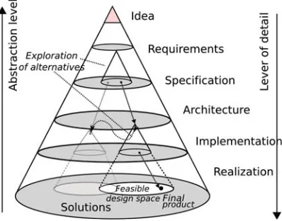
The process of designing a system can be described using the pyramid shown in Figure 1.1. The figure splits the design process in several stages. The design process starts at the top and by making choices a lower stage is reached and more detail is achieved. The choices made during the design result in different final products.
[image:10.612.195.394.418.574.2]The pyramid model is useful for FPGA design because trade-offs need to be made during design in e.g. accuracy, development time, FPGA resource usage, timing and performance. The large capacity of the Virtex-5 allows for this sort of trade-off studies.
Figure 1.1: System design process (Corporaal, 2006; Groothuis and Broenink, 2009)
Figure 1.2: CE design flow (Broenink et al., 2007)
The figure shows a design flow developed within the Control Engineering group (CE). The design flow consists of four design phases:
• Physical System Modeling: A model of the physical system is designed.
• Control Law Design: The model of the physical system is used to create a controller for controlling the physical system.
• Embedded System Implementation: In this step the model is prepared for implemen-tation on a hardware platform. Effects of operations like sampling, digital-to-analog / analog-to-digital conversion are included into the model.
• Realization: The system is transferred to hardware and tested on the physical system.
The result of each design phase is analyzed. In the first three design phases this is done by simulation. By simulation, it can beverified whether the model, as it has been written down in the simulation program, behaves as it was designed to do so. For this check, test simulations can be run to judge the behavior of the model under particular circumstances, like equilibrium, step response and transient response. Important aspects to look at are the shape of the curves and the value range of the variables. During the realization phase measurements on the real physical system can be performed. These measurement results can be compared to the simulations results, this is calledvalidation.
The verification step is critical as it allows for stepwise refinement of the model. This means that a problem is divided into small, manageable subproblems. Solving of such a subproblem leads to a more complete answer to the whole problem e.g. the design of a model.
The prefered design for mechatronic design within CE is 20-sim (Controllab Products, 2009). It can be used during all four design phases from modelling a physical system to C/C++ code generation when the target hardware platform uses a general purpose processor. When the code has to be executed on an FPGA, the 20-sim code generator cannot be used. This is because FPGAs are not programmed using C/C++ but using a
Hardware Description Language(HDL) and 20-sim does not provide a code generator for this.
In previous projects targetting an FPGA, the design was ported to Handel-C during the Realization phase. Handel-C is a hardware desciption language based on ANSI-C with language extensions for paralellism inspired by CSP. It would make sense to use Handel-C for this project but it proved not to be suitable:
• The Handel-C tools do not provide glue logic for interfacing Handel-C designs with a PowerPC CPU; writing your own Handel-C/VHDL interfaces for this is possible but it is a lot of work.
in previous CE projects. This method is not suitable for a large FPGA due to long synthesize times.
• The future of Handel-C is uncertain after the company which developed it (Agility Design Solutions, 2009), has been acquired by its competitor Mentor Graphics.
This project focusses on the ”Embedded Control System Implementation” and ”Realiza-tion” phases. Models of a plant and controller are reused from previous projects and are modified were needed. FPGA design tools from Xilinx will be used to realize the design in the Virtex-5.
1.4 FPGA terminology
In electrical engineering and computer science some terms have a different meaning. One such term is hardware which in case of electrical engineering refers to components like resistors or circuit boards while in case of computer science the content used to configure an FPGA is considered hardware as well. To prevent confusion within CE, terminology is introduced here which is used throughout the rest of this report. The terminology is introduced by explaining CPUs and software first.
A CPU is a device which can execute a fixed number of operations like additions and multiplications. The tasks which a CPU has to perform are contained in a software program. A software program is a sequence of instructions which defines the operations a CPU has to perform in a specified order.
An FPGA is a parallel device of which the functionality can be configured at device startup. Both software and ’FPGA functionality’ are expressed in a human readable language which is compiled to respectively a software program or an FPGA programming file. The main difference is that an FPGA programming file does not contain instructions but it defines a structure of a digital circuit. Depending on performance constraints specified to a HDL compiler more operations are performed in parallel, which takes more FPGA building blocks, or operations are performed sequentially to save FPGA building blocks. If writing software is a 1-dimensional problem in execution time, FPGA programming is a 2-dimensional problem in FPGA area and execution time.
In this report the content which is used to configure an FPGA is calledconfigware instead of hardware (Hartenstein, 2006).
Vendors of FPGAs provide pre-built configware blocks in order to save design time. Pre-built configware blocks are calledIntellectual Properties (IPs) or soft-cores. The last term is used in this report. The term hard-core exists as well and it refers to fixed blocks integrated into FPGAs like DSP blocks or CPU cores.
1.5 Report outline
This report provides some background information on various topics regarding the Xilinx hardware and software. Some of the chapters can be seen as a continuation of these background chapters but they cover the work carried out in this assignment e.g. work in order to get the ML510 board working. The choice was made to place chapters containing own work after the corresponding background chapter.
2 ML510
In this chapter an overview of the capabilities of the ML510 is given. The first two paragraphs give a look at the ML510 and the Virtex-5 FPGA from a computer architecture point of view. The third section gives an overview of the User I/O ports of the ML510. The fourth section gives an overview of supported operating systems. The last section compares the Virtex-5 FPGA with FPGAs used in previous CE projects.
2.1 Overview
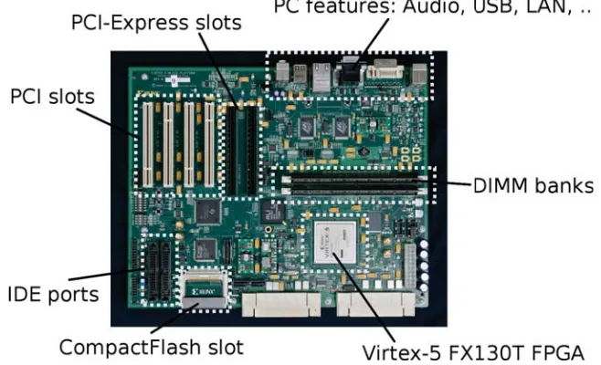
[image:14.612.129.458.287.487.2]A picture of the Xilinx ML510 development board is shown in Figure 2.1. At first glance the board looks like an ATX-sized PC motherboard with features common on PC moth-erboards like PCI slots, IDE ports, DIMM banks and more. Closer inspection reveals that there is no general purpose processor like a x86-processor on the board but a Virtex-5 FX130T FPGA.
Figure 2.1: Xilinx ML510 FPGA board
General FPGA development boards offer a large number of User I/O pins in combination with communication interfaces like UARTs and Ethernet. The ML510 offers this as well but also offers a large amount of features normally found in PCs. An overview of the features of the ML510 is given below:
• FPGA: Virtex-5 FX130T
• CPU: 2x IBM PowerPC 440 core (inside the Virtex-5 FX130T)
• Memory: 2x DIMM banks for DDR2 memory (by default each contains 512MB • Expansion slots: 4x PCI, 2x PCI-Express
• Storage: 1x CompactFlash interface, 256Mbit onboard Flash, 2x IDE, 2x Serial ATA • LAN: 2x Gigabit Ethernet physical layers
• Video: 1x DVI-I, max resolution 640x480
• Audio: AC97 audio with headphone and microphone ports • I/O-ports: 2x RS232, 2x PS/2, 2x USB 1.1
• User I/O: 124 GPIO pins, 4x debug LED/switch
FPGA. Xilinx and their partners ship a large number of different soft-cores which can be flashed inside the FPGA. This way the ML510 can be configured to the requirements of the designer.
In case of Ethernet: the ML510 contains two onboard Ethernet physical layers. Different Ethernet soft-cores are available, which allow for realization of different types of Ethernet cards. Two of the available Ethernet soft-cores are a Gigabit Ethernet core by Xilinx and a real-time Ethernet core EtherCAT core by Beckhoff (Beckhoff, 2008).
2.2 Virtex-5 FX130T FPGA
This section gives an overview of the Virtex-5 FX130T FPGA and two of its components namely DSP blocks and the embedded IBM PowerPC 440 processor cores.
2.2.1 Overview
Xilinx offers two families of FPGAs: the low-cost Spartan and the high-end Virtex. A recent Virtex family is the Virtex-5. It is made using 65nm technology and it offers various architectural improvements over previous Xilinx FPGAs.
The most significant change in the Virtex-5 over previous Xilinx FPGAs is the design of its logic cells. In previous Xilinx FPGAs, these were made up of a 4-input lookup-table (LUT) in combination with a flip-flop and some other logic. The Virtex-5 uses larger logic cells, each consisting of 6-input LUT paired with a flip-flop and the other logic. Four logic cells are grouped together in slices.
A 6-input LUT has a capacity of26 entries which is equivalent to four traditional 4-input LUTs, which have24 entries each. Not all designs can take advantage of the larger LUTs. For example basic bitwise operations which need less than six inputs, do not use a 6-input LUT up to its maximum capacity. Xilinx claims that on average one Virtex-5 logic cell is equivalent to 1.6 traditional logic cells (Xilinx, 2007). This factor will be used throughout this report when comparing resource usage with previous FPGA designs.
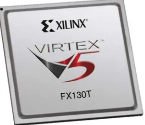
[image:15.612.234.380.555.681.2]Within the Virtex-5 family, there are five product lines each optimized for a different application. The differences can be found in the number of logic cells, the number of DSP blocks and the number of high-speed communication links. The FPGA on the ML510 is a Virtex-5 FX130T (see Figure 2.2) which belongs to the FXT product line. This product line is optimized for embedded processing and offers one or more embedded IBM PowerPC 440 processors in combination with a moderate amount of logic cells and DSP blocks. The Virtex-5 FX130T is one of the largest Virtex-5 FXT models.
An overview of the features of the Virtex-5 FX130T is given below: • Slices: 20,480 (contains logic cells and flip-flops)
• Logic cells: 81,920 6-input LUTs (equivalent to 131,072 traditional 4-input LUTs) • Flip-flops: 81,920
• Maximum operating frequency: 550MHz • DSP blocks: 320x DSP48E
• Processor block: 2x IBM PowerPC 440 cores
• Block RAM: 298 blocks of 36kbit for a total of 10,278kbit
• Hard-core memory controller with support for DDR2 using soft-core bridge • LAN: 6x 10/100/1000 Ethernet MAC blocks
• High-speed serial I/O: 20x RocketIO transceivers capable of 150Mbps to 6.5Gbps
2.2.2 DSP48E block
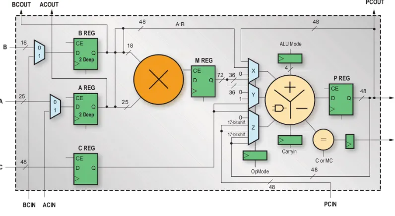
Algorithms make frequent use of arithmetic operations like additions, subtractions and multiplications. These operations can all be implemented in logic cells, but the use of logic cells has two disadvanages. First, when a high number of bits is needed (e.g. for accuracy) a large number of logic cells is required. Second performance of a design implemented solely using logic cells is limited. This is because a structure like a multiplier can require hundreds of logic cells which all have to be connected. Connecting these using an internal network reduces performance. For this reason DSP blocks which can perform arithmetic and logic operations have been added to modern FPGAs.
The Virtex-5 FX130T contains 320 DSP48E blocks which can operate at a frequency upto 550MHz. The DSP blocks are spread in columns and rows over the FPGA. Within a column DSP blocks are connected to each other using an internal network.
[image:16.612.96.494.430.648.2]A DSP block (see Figure 2.3) consists of a 2-complement 25x18 multiplier in parallel with an integrated 48-bit ALU and logic for buffering and signal routing.
Figure 2.3: Virtex-5 DSP48E block, image (Przybus, 2007)
PCIN or from the output data of the multiplier. It can also be fed with previous results stored in the P register and in this way it acts like an integrator.
There are three ways using which DSP blocks can be used in a design. First, smart FPGA synthesis tools are able to automatically realize logic and arithmetic operations using DSP blocks when it makes sense to them. Second, the designer can explicitly instantiate DSP blocks in his design but this requires additional work. The work includes configuration of multiplexers and other logic in the DSP block. Third, design tools can offer wizards for the creation of filters and floating-point cores which use the DSP blocks internally. The DSP block can be used in various applications, two of these are explained here. One such an application is the creation of digital filters. Digital filters consist of a large number of stages and each stage performs multiplications and subtractions. Each stage can be mapped on a single DSP block. Using PCIN and PCOUT multiple stages can be chained together.
A second application of the DSP block is the implementation of floating-point. Xilinx provides a floating-point core wrapper named Floating-Point Operator (Xilinx, 2009a) which can be used for implementing single and double-precision floating-point. For single-precision, the floating-point wrapper requires two DSP blocks and the wrapper can operate upto 410MHz. Each calculation requires multiple clock cycles. For instance a multipli-cation takes 8 clock cycles and an addition takes 11. The effective operating frequency of the wrapper is approximately 50MHz (=410MHz/8) for multiplications and 40MHz (=410MHz/11) for additions. The effective operating frequency can be increased by us-ing more DSP blocks. For example, doublus-ing the operatus-ing frequency requires twice the number of DSP blocks.
2.2.3 IBM PowerPC 440 CPU core
The Virtex-5 FX130T features two separate IBM PowerPC 440 cores. PowerPC is a RISC based processor architecture developed by IBM in coorperation with Apple and Motorola (IBM, 2009). These days PowerPC based CPUs are used in all sorts of devices ranging from consumer devices, like Wii, Playstation3 and Xbox360 to high performance servers and embedded systems. For integration into SoCs, IBM offers embedded PowerPC cores. This type is used in the Virtex-5 FXT series.
The PowerPC 440 is a 32-bit big-endian CPU, based on the PowerPC Book-E specification for embedded processors (IBM, 2003). This specification defines a common subset of the PowerPC architecture which all Book-E designs must implement. Extra functionality like 64-bit support or a hardware floating-point unit is optional.
The Book-E specification also defines an interface for anAuxiliary Processor Unit (APU) which can hook into the execution engine of the processor for the creation of custom CPU instructions. Xilinx for instance offers a PowerPC-compatible soft-core floating-point unit which makes use of it.
A list of features is shown below.
• Architecture: 32-bit PowerPC (RISC) • Endianness: Big-Endian
• Clock frequency: upto 475MHz1 • Integrated memory management unit
• APU-bus for creation of custom CPU instructions • Floating point: available using APU-connected soft-core
Xilinx has added logic around the PowerPC 440 core for high-performance, low latency
1In the FX130T FPGAs with the fastest speed grade PowerPC 440 cores can run upto 550MHz, the
access to system memory and periperhals inside the FPGA. The resulting hard-core em-bedded processor block is shown in Figure 2.4. The block consists of the PowerPC 440 core, an APU-bus for interfacing with co-processors,Device Control Registers (DCR) and a Crossbar interface.
Figure 2.4: Embedded PowerPC 440 processor block with Crossbar (Abramson et al., 2008)
The Device Control Registers are a special type of registers which are visible from inside the CPU core (and also have their own special CPU instructions) but are actually implemented outside the CPU core as a soft-core. The registers are meant as a control interface for busses and custom peripherals implemented in FPGA logic. Some soft-cores like the Xilinx Ethernet core and the Xilinx VGA core use the DCR interface.
The Crossbar is used by both the CPU and the FPGA to access system memory and peripherals. A more detailed diagram of the Crossbar interface which illustrates this is shown in Figure 2.5. The light colored areas are inside the FPGA, the DDR2 memory is outside the FPGA in the ML510 dimm banks. The Crossbar has five input connections (on the left) and two output connections (on the right).
Figure 2.5: Crossbar with peripherals attached (Abramson et al., 2008)
wide. Three of the PLB inputs, named ICURD, DCURD and DCURW, are used by the CPU for respectively reading instructions, reading data and writing data. The other two ’PLB Slave’ inputs can be used as a PLB as well but they can also be used as a LocalLink DMA port as shown in Figure 2.4. A LocalLink interface is used by high-speed devices like Ethernet cores.
The two output connections are connected to respectively aMemory Controller Interface
(MCI) and a PLB to which PLB slave devices can be attached.
Peripherals connected to the input connections are called masters. They can initiate data read or write transactions on the Crossbar. As part of a transaction a master provides a memory address. Based on this address, the Crossbar forwards a transaction to either the MCI or aPLB Master (MPLB). In case of the ML510, the MCI is wired to DDR2 system memory using a soft-core memory controller. The PLB Master is interfaced to PLB slave devices for GPIO and UART.
Communication between a soft-core in the FPGA and the CPU can be done in various ways. First of all a soft-core can be connected as a PLB slave device to the MPLB. The crossbar is then able to provide a direct connection between soft-core and a master like the CPU. Another method is to use shared memory. For this the soft-core uses a PLB Slave or a LocalLink to access system memory and writes his data there. The CPU can read it there but there would be no direct connection. Performance can be higher because both soft-core and CPU do not have to be synchronized.
2.3 User I/O
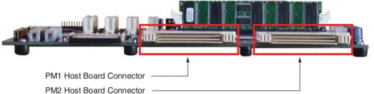
[image:19.612.116.501.462.559.2]The ML510 board has been designed for high-performance embedded applications. For this reason it offers various high-speed communication busses like PCI, PCI-Express, S-ATA and Ethernet. Standard development boards offer pin headers for interfacing with custom peripherals. These pin headers are not suited for high-speed communication at hundreds of megahertz and for this reason Xilinx provides two ’Xilinx Personality Module’ (XPM) interfaces named ’PM1’ and ’PM2’ as shown in Figure 2.6.
Figure 2.6: ML510 XPM connectors
The connectors as shown in Figure 2.7 are Tyco ’Z-Dok’ connectors. They are designed for high-speed differential communication at bitrates upto 6.5Gbps and for this reason they are expensive. In control applications the highest frequent signals are needed for Pulse Width Modulation (PWM). When using a PWM frequency of 10kHz, a duty cycle of 1% corresponds to a bitrate of 1MHz, so the Z-Dok connectors can operate at three orders of magnitude higher bitrate than needed.
with an opposite sign and the signal level is not relative to ground. LVDS is less sensitive to disturbances and for this reason used for high-frequent signals. Each LVDS pair can be used single-ended as well and in this way act like a normal pin. While most pins use 2.5V, a small number of pins is also suited for 3.3V.
Figure 2.7: Tyco Z-Dok connectors
Both PM1 and PM2 ports combined provide the ML510 with upto 158 I/O pins. The features of each connection are given below. The PM1 connector provides the following signals:
• 8 high-speed RocketIO serial links
• 3 LVDS pairs at 2.5V (can be used as 6 single-ended I/O at 2.5V) • 1 LVDS clock pair at 2.5V
• 12 single- ended I/O at 2.5V • 26 single-ended I/O at 3.3V • 1 single-ended clock at 2.5V • 1 pin not connected
The PM2 connector on provides the following signals:
• 39 LVDS pairs at 2.5V (can be used as 78 single-ended I/O at 2.5V) • 1 single-ended clock at 2.5V
• 1 pin not connected
2.4 Operating system support
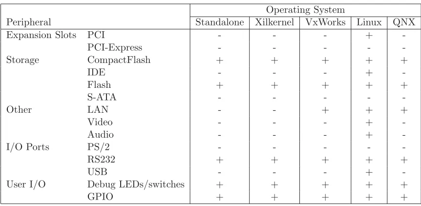
The availability of a PowerPC 440 CPU inside the Virtex-5 FX130T allows the use of operating systems with PowerPC support. The Xilinx ML510 is officially supported by three operating systems: Xilinx standalone, Xilinx Xilkernel and VxWorks. Other Xilinx boards based on a similar FPGA as used on the ML510 are supported on Linux and QNX as well. Due to support for other Virtex-5 FXT FPGAs in Linux and QNX, there is also a limited amount of unofficial support for the ML510.
As part of this assignment Linux support has been added for the ML510 and this is available in the Linux 2.6.31 kernel (see chapter 3). The performed work includes adding support of peripherals not available on other Xilinx boards which are supported on Linux. An overview of the features of the different operating systems kernels is shown in Table 2.1. In case of Linux the table reflects the features as supported in Linux 2.6.31. For QNX the table reflects the features supported on the ML507.
Operating System kernel
Feature Standalone Xilkernel VxWorks Linux QNX
Console + + + + +
Memory management – – + + +
Timers – + + + +
Real-time support – – + ? 2 +
Multithreading – + + + +
Networking +/– +/– + + +
Filesystem support +/– +/– + + +
Table 2.1: Features of operating system kernels
It can boot the CPU and bring up a console with input and output on the UART. From software there is access to all board periperhals including flash memory, Ethernet and user I/O using user mode libraries for which Xilinx provides a few examples. The Xilinx Xilk-ernel is similar to Xilinx Standalone but adds support for Posix threads and timers. Both Xilinx Standalone and Xilinx Xilkernel are suited for running basic control algorithms, but since each kernel provides only limited functionality the user needs to guarantee real-time behavior and provide memory management.
VxWorks (Wind River Systems, 2009) is a commercial, closed-source, real-time operating system developed by Wind River Systems, a subsidiary of Intel. This operating system supports a large number of hardware platforms and it is widely used by the industry in aerospace, automotive, military and telecommunication applications.
Linux (Torvalds, 2009) is an open-source, UNIX-compatible operating system with support for a large number of hardware platforms. This operating system is frequently used for real-time applications within CE. This requires the use of real-time patches like RTAI (DIAPM, 2009) or Xenomai (Xenomai Project, 2009) patches. These are also available for the PowerPC 440 architecture but whether they work on the ML510 is not known. Most likely changes in the Xilinx interrupt controller driver are needed.
QNX (QNX Software Systems, 2009) is a commercial, real-time, operating system for use in embedded systems. This operating system uses a micro-kernel which is responsible for task creation, scheduling, interprocess communication and interrupts. All other tasks are handled using ’servers’ in user-space, which are applications running in the background. This allows disabling of features without recompiling the operating system. The source code of the QNX kernel is available for non-commercial use.
An overview of the peripherals supported by each operating system is given in Table 2.2. As is shown in the table, Standalone and Xilkernel offer basic I/O support and access to flash storage. VxWorks and QNX add support for LAN. Linux supports most periperhals including including Audio, IDE, PCI, USB and Video.
Peripherals unsupported by any of the operating systems are: PCI-Express, S-ATA and PS/2. For PCI-Express there is a soft-core but no driver for it has been written. In case of ATA there is no ATA controller core available. The reason the board contains S-ATA connectors at all is because they allow for creation of a high-speed communication link using commercial-of-the-shelf cables. PS/2 is part of a ALI M1533 PCI chipset and depends on PCI support. Linux support for it can easily be added but it is not available at this point.
2Real-time Linux patches (RTAI and Xenomai) are available for PowerPC 440 Linux, but whether they
Operating System
Peripheral Standalone Xilkernel VxWorks Linux QNX
Expansion Slots PCI - - - +
-PCI-Express - - - -
-Storage CompactFlash + + + + +
IDE - - - +
-Flash + + + + +
S-ATA - - - -
-Other LAN - - + + +
Video - - - +
-Audio - - - +
-I/O Ports PS/2 - - - -
-RS232 + + + + +
USB - - - +
-User I/O Debug LEDs/switches + + + + +
[image:22.612.93.524.71.282.2]GPIO + + + + +
Table 2.2: ML510 peripheral support in operating systems
2.5 Virtex-5 compared to FPGAs used in previous CE projects
The preceeding sections described the Virtex-5 from a computer architecture point of view. It is described using quantities like logic cells and DSP blocks. This section illustrates the use of the Virtex-5 for control. This is done by estimating the FPGA resource usage of a control design, previously made for a different FPGA, if would be transferred to a Virtex-5. The results of a recent FPGA project on floating-point based control of the Production Cell setup (Sassen, 2009; Groothuis and Broenink, 2009) are used as a reference.
The FPGA used for the control of the Production Cell is a Xilinx Spartan-3 XC3S1500. The Spartan-3 is based on a less modern architecture than the Virtex-5 and it offers less features but at a lower price. A comparison between the two FPGAs is shown in Table 2.3.
FPGA
Feature Spartan-3 XC3S1500 Virtex-5 FX130T
Logic cells 29,952 131,0723
Flip-flops 29,952 81,920
Maximum operating frequency 200 MHz 550 MHz
Processor cores 0 2
DSP blocks 0 320
Multipliers 32 04
Block RAM 576kbit 10,278 kbit
Table 2.3: Comparison between Virtex-5 FX130T and Spartan-3 XC3S1500
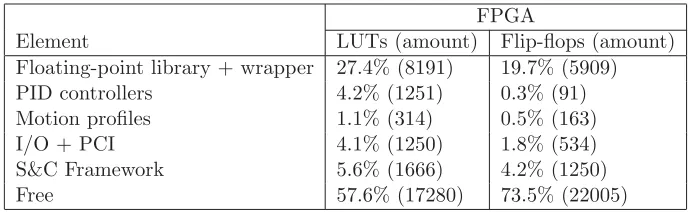
The Production Cell setup consists of six motors and each motor requires a PID controller and a motion profile. The setup uses a sample frequency of 1 kHz. The Spartan-3 did not offer enough FPGA resources for a parallel floating point implementation of six PID controllers. In order to fit the design into the Spartan-3, a single PID controller block was designed in such a way that it could be reused for all six PID calculations. The same was done for the calculation of motion profiles. The results are shown in Table 2.4 (Groothuis and Broenink, 2009).
3Equivalent number of 4-input LUTs
FPGA
Element LUTs (amount) Flip-flops (amount)
Floating-point library + wrapper 27.4% (8191) 19.7% (5909)
PID controllers 4.2% (1251) 0.3% (91)
Motion profiles 1.1% (314) 0.5% (163)
I/O + PCI 4.1% (1250) 1.8% (534)
S&C Framework 5.6% (1666) 4.2% (1250)
Free 57.6% (17280) 73.5% (22005)
Table 2.4: Estimated FPGA resource usage of the Production Cell on a Xilinx Spartan-3 FPGA
The results in the table are estimated based on compile logs of the Handel-C compiler. As can be seen in the table a large number of LUTs and flip-flops is taken by a floating-point library. The design contains this library for carrying out the majority of the calculations for both the PID controllers and motion profiles. The compiler has placed a large portion of the FPGA resources which were only used in the PID controller or Motion profile code to the floating point library. For estimating how many times the design can fit into the Spartan-3 the FPGA resource usage of these three parts needs to be added together. In total the sequential design can fit the Spartan-3 twice but it is not big enough to fit it six times.
The Production Cell design could be moved changes in the pin-out to the Virtex-5. This recompilation has been attempted but during synthesis a lot of compile errors were en-countered which would take a lot of effort to fix. Instead, the results are calculated out of the Spartan-3 results using the approximation that one 6-input Virtex-5 LUT equals 1.6 Spartan-3 LUTs. This means that the amount Spartan-3 LUTs has been divided by 1.6, the number of flip-flops stays the same. The results are shown in Table 2.5.
FPGA
Element LUTs (amount) Flip-flops (amount)
Floating point library + wrapper 6.3% (5120) 7.2% (5909)
PID controllers 1.0% (780) 0.1% (91)
Motion profiles 0.2% (200) 0.2% (163)
I/O + PCI 1.0% (780) 0.7% (534)
S&C Framework 1.3% (1040) 1.5% (1250)
[image:23.612.137.487.73.179.2]Free 90.2% (74000) 90.3% (73973)
Table 2.5: Calculated FPGA resource for the Production Cell using a Xilinx Virtex-5 FPGA
2,000,000 PID calculations a second or 2,000 each sample period (1ms). The Virtex-5 contains 320 DSP blocks, so it allows for 320,000 PID calculations per sample period or 320,000,000 per second!
The motion profiles could also be realized using DSP blocks and this would save additonal LUTs and flip-flops. An even better way would be to store motion profiles in memory blocks which are filled by the PowerPC core at startup. This way only a small number of LUTs and flip-flops would be needed to create a bus interface to the processor, the rest would be located in block memory of which the Virtex-5 offers a large amount. An advantage of this approach would be that for a motion profile with a different shape only the software needs to be changed and no changes to the FPGA design have to be made. The described redesign of the Production Cell using Virtex-5 functionality would require only a few percent of LUTs and flip-flops since PID controllers and motion profiles can be implemented efficiently using DSP blocks and block memory. In total 320,000 PID calcu-lations could be calculated in a single sample period which is enough for 320,000/6=53,000 Production Cell setups. Though at some point the number of User I/O pins (158) becomes a limitation and serial communication busses e.g. EtherCAT must be used.
3 Preparation of the ML510 for control applications
The first half of this assignment is devoted to making the ML510 usable for CE projects. This work consisted of programming, hardware testing and documenting all steps on the CE wiki.
The first section describes the work carried out for adding ML510 support to the Linux kernel. The second section describes integration of the ML510 Linux code with Embryo. The third section describes work on an external I/O board which provides the ML510 with I/O pins for interfacing with external periperhals like a plant.
3.1 Linux kernel
Linux is the most used operating system at CE for use in embedded control systems. The availability of Linux support for the ML510, as claimed at the launch of the ML510 (Xilinx, 2008b), was one of the reasons for acquiring the board. After the board had arrived and tests were performed, it appeared that no Linux support was publicly available for the ML510.
Xilinx had written ML510 Linux support for an outdated Linux kernel but they decided not to release the code because it was incomplete and would have to be rewritten for use with modern Linux kernel versions which they decided not to do so.
Besides the ML510, Xilinx offers other FPGA boards based on the Virtex-5 FXT. One of these is the ML507 which contains a smaller FPGA with a single PowerPC 440 core and less onboard features compared to the ML510 for instance it lacks PC functionality like IDE, PCI, and VGA support but it does provide standard pin headers for I/O. Xilinx provides official support for the ML507 in Linux.
Due to similarities between the ML507 and the ML510, it was decided to port Linux to the ML510 and take the ML507 code as a starting point. In order to prepare the ML510 for vision, which was the intended test case for this assignment, work was also done on adding support for the PC features offered by the ML510.
The performed ML510 Linux work includes:
• Creation of a Linux-compatible configware package for the ML510. • Adopting ML507 Linux code for use on the ML510.
• Writing of a PCI driver for the ML510 to make previously unsupported board func-tionality available.
• Submission of the ML510 Linux work to the Linux developers for inclusion in the official Linux kernel distribution.
The remaining of this section describes the ML510 Linux work in detail. Instructions for installing Linux on the ML510 can be found in Appendix B.
Before the ML510 is able to run software, configware needs to be loaded into it for inter-facing the CPU to a memory controller and setting up board peripherals. For the ML507, Xilinx provides a pre-built configware package to boot Linux. For the ML510 such a Linux-compatible configware package had to be developed from scratch, see Appendix B.1.
• No debug output shown on the console
The most common issue is that no output appears on the UART which is used as a serial console for input and output. In general this issue is caused either by incorrect system information provided by a DTS-file to the Linux kernel or by a Linux kernel panic which occurs before the console is initialized. The first issue can be fixed by verifying by hand whether the DTS-file is correct. The second issue is hard to debug because no debugger is available, which means that the designer needs to act as a debugger. In this project special UART debug code was added to the Linux kernel boot process to reveal the kernel panic log.
• Linux kernel panic
A Linux kernel panic occurs when a driver or other part of the Linux kernel crashes. In general such issues are caused by driver bugs caused by null pointer exceptions or deeper issues. The kernel crash log and related driver code needs to be analyzed to find the root of the problem.
The two categories of issues described above give an idea about the issues encountered. In general debugging crashes on the ML510 is very time consuming and depending on the issue it takes hours or even days.
In order to prepare the ML510 for robotic applications a PCI driver was written to make previously unsupported PC functionality of the ML510 available. The driver allows the use of the on-board PC functionality but it also allows the use of PCI add-on cards e.g. a FireWire add-on card for interfacing with a video camera. Details on the PCI driver can be found in Appendix A.2.
The finished ML510 Linux code has been submitted for inclusion into the official Linux kernel distribution and is part of the Linux 2.6.31 which is to be released in September 2009. The inclusion of the code in the Linux kernel is important because it ensures that the code gets maintained and it proves the quality of the written code. Before any code enters the Linux kernel, it is reviewed by other developers and they provide feedback for improving the code. In general, a number of design iterations is needed before the code is considered clean enough for inclusion in the Linux kernel. In this case three iterations were required.
In total it has taken approximately three months for writing all ML510 Linux code. The process of getting the code integrated into the official Linux kernel distribution took an-other two months.
3.2 Embryo
Within CE a variety of different hardware platforms is used. Most of these run a Linux distribution named Embryo developed by ir. M. Groothuis from CE. Embryo is a small, embedded Linux distribution build on top of OpenWrt (OpenWrt, 2009) which is fre-quently used on wireless routers. As part of this assignment ML510 support has been added to Embryo. Below Embryo and the ML510 Embryo work are described. Installa-tion instrucInstalla-tions for Embryo can be found in Appendix B.
Embryo itself is a set of scripts and configuration files which automate all compilation tasks for building an embedded Linux distribution. These tasks include:
• Downloading source code of compilers, the Linux kernel, libraries and tools. • Building of cross-compilers.
• Configuration and building of the Linux kernel. • Compilation of Linux libraries and tools. • Creation of a Linux root file system.
system like Linux or Mac OS X. The first task is to configure the Embryo distribution. This includes the selection of hardware platform, a set of libraries and the tools to be bundled with the Embryo installation. After that Embryo downloads and compiles the source code of compilers, the Linux kernel and the selected libraries and tools. The compiled Linux kernel, libraries and tools can then be installed on a memory card or a hard disk for loading on the embedded hardware platform.
In case of the ML510, Embryo already had support for the PowerPC 440 architecture. Most work focused on configuration files for a ML510 Linux kernel and integration of a compiled Linux kernel with an FPGA programming file to allow the ML510 to launch Embryo. Details on this integration can be found in section 5.3.
3.3 ML510 I/O board
As explained in section 2.3, the ML510 lacks I/O pin headers which are needed for in-terfacing with custom peripherals like a plant. An extension board is needed to interface the Z-Dok connectors of the ML510 to I/O pins. Such a board has been designed by the Electronic Systems group of the Technical University of Eindhoven (TU/e) because they have also required access to I/O pins on a ML510 board. An empty PCB of the ML510 I/O board has been acquired from the TU/e. This section describes the board and the work needed to get it working for a CE setup.
The demonstrator which had to be interfaced to the ML510 at the TU/e, was a setup similar to the Production Cell. Originally this setup was controlled by a PLC and now it needs to be controlled by an FPGA. Their requirements for the I/O board were:
• Digital high level of 24V
• Signal frequency in the order of 1 kHz
• Prevent the test setup from damaging the FPGA
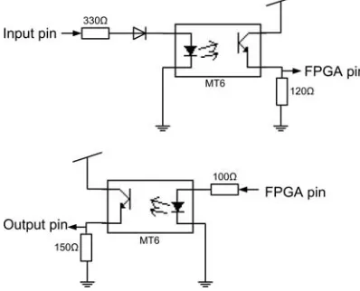
[image:27.612.208.407.530.691.2]Based on these requirements an I/O board was built which provides access to 78 pins of which one half is for input and the other half for output. The board uses optocouplers to isolate the FPGA from the setup. The type of optocouplers used in the design is meant for transmission of analog signals with an analog bandwidth of 100kHz. For use in setups as used within CE, the optocouplers are not ideal because PWM signals which are used for digital-to-analog conversion require a frequency of several MHz for high accuracy. Other types of optocouplers, optimized for digital I/O at high frequencies, are available but they use a different pinout and require different biasing, so they cannot be used on this board.
For interfacing with a CE setup modifications were made to the circuitry to get it to operate at 5V and component values were adjusted to improve performance of the optocouplers for use with PWM signals. A diagram of the circuitry is shown in Figure 3.1. With these modifications the I/O board is usable but the optocouplers severly limit the accuracy of input and output signals. For instance when outputting a square wave at a frequency of 100kHz with a 50% duty cycle, the signal is high for 55% instead of 50%. This results in losses in accuracy during digital-to-analog-conversions. Similar issues occur for the input pins. Another problem, only limited to inputs pins of the I/O board, is that optocouplers have current inputs while within CE voltage signals are used. A buffer chip is required to be able to drive the optocouplers.
4 Xilinx Design flow
The first section of this chapter introduces the concept of hardware/software co-design. Xilinx offers various FPGA design tools and multiple design flows (using their tools) for hardware/software co-design. For the creation of designs consisting of an embedded CPU and configware, the design flow recommended by Xilinx is build around a tool named
Platform Studio Embedded Development Kit (EDK). Development of software (SW) and configware (CW) takes place in specialized tools outside EDK, the EDK is used for their integration into the overall system design. The EDK is described in section two.
The third section describesPlatform Studio SDK which is used for software development. Xilinx offers two tools for the development of configware namely ISE Foundation and
System Generator for DSP (SysGen). The first tool, described in section four, is the one recommended by Xilinx for obtaining the best performance and lowest FPGA resource usage at the cost of a large design effort. The second tool, described in section five, requires a smaller design effort at the cost of performance and FPGA resource usage.
4.1 Hardware/Software co-design
When creating a design which consists of a CPU and an FPGA, decisions have to be made on which parts of an algorithm to implement in configware and which in software. Good candidates for implementation in configware are the parts which are either computation intensive or which have hard real-time requirements.
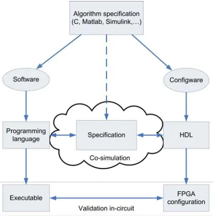
The process of paritioning an algorithm in configware and software is illustrated in Fig-ure 4.1. It starts with a specification of the algorithm for example in C, MATLAB, Simulink or 20-sim. Next, the algorithm should be analyzed by the designer to discover timing critical or CPU-intensive parts. A profiling tool can obtain statistics on how much CPU time is spent in different parts of the algorithm. This is done by analyzing the al-gorithm when it is running on a CPU. In the end, the decision on how to partition the algorithm lies by the designer.
When a partioning in configware and software has been made, both parts can be imple-mented using respectively a hardware description language (HDL) and a programming language. During development co-simulation can be employed to test the individual parts against the algorithm specification or against each other. Co-simulation (Damstra, 2008; Colenbrander et al., 2008) is a type of simulation in which models can be simulated to-gether while each uses a different simulation engine. This can prevent late integration problems.
Figure 4.1: Partitioning of an algorithm in configware & software (Colenbrander et al., 2008)
Figure 4.2: Different ’X’-in-the-loop simulation types, image from (Oosterom, 2006) The four types of ’X’-in-the-loop are described below:
• Model-in-the-loop: models of a plant and control algorithm are connected in a loop and are simulated on the same development PC, this is normal simulation.
• Software-in-the-loop: control algorithm runs as an executable on the development PC, plant and I/O are simulated on the development PC.
• Processor-in-the-loop: control algorithm runs as an executable on the target proces-sor, plant and I/O are simulated on the development PC.
• Hardware-in-the-loop: control algorithm runs on target processor, non-simulated I/O over wires, plant simulated on the development PC in real-time.
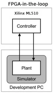
Figure 4.3: FPGA-in-the-loop simulation
4.2 Hardware/software co-design using Platform Studio EDK
The primary Xilinx design tool for hardware/software co-design is Platform Studio Em-bedded Development Kit. The program is used for overall system development and project management. Development of software and configware takes place in specialized tools, the EDK is used for their integration into the overall system design.
The program ships with a collection of templates and configware for the creation of an embedded design. A new foundation for an embedded design is created using a wizard calledBase System Builder (BSB). At the start of the BSB wizard a template of the target FPGA board, for example the ML510, has to be loaded. This template provides the wizard with information about the target board (e.g. available CPU, available configware and pin locations). The BSB wizard can then be used to configure the target board with a CPU and the peripherals needed to obtain a bootable system. All hardware information is stored in aMicroprocessor Hardware Specification file (MHS).
The base system can be extended with user created configware or with configware shipped with the EDK. Additional configware needs to be integrated into the overall system de-sign. Integration consists of connecting communication busses, the assignment of memory addresses and mapping of input/output pins to FPGA pins. The EDK automates most of this integration work but pin mapping has to be done manually. This is done by adding location constraints, which are the mappings of FPGA nets to FPGA pins, to a User Constraints File (UCF).
The EDK can be used to set up a simulation environment in which the completed system can be simulated. Different types of simulation can be carried out ranging from fast but inaccurate behavioral simulations to detailed timing-accurate simulations. The simulation time increases with the amount of detail requested. In order to decrease simulation time, the EDK ships with simulation models of busses, configware and processors but even then simulation time can be long. It is recommended to only verify the behavior of individual, custom designed cores and to verify behavior of the complete system on-target.
The ML510 contains a hardware based boot loader namedSystem Advanced Configuration Environment (SysACE). Its task is to initialize the FPGA and CPU at board startup. SysACE boots the ML510 from ACE-files which are stored on a CompactFlash card. An ACE-file is the integration of pre-compiled software in theExecutable and Linkable Format
(ELF) with aFPGA bitstream programming file (BIT).
three columns each representing a different program. The steps performed using EDK are numbered 1.x and the software and configware blocks have respectively the numbers 2 and 3. These last two numbers are also used for the numbering of steps carried out in software and configware design flows presented in the rest of this chapter and in chapter 5. The numbering schemes used for respectively software and configware are [2.y.x] and [3.y.x], where ’y’ is used for numbering the design flow and ’x’ for numbering a step within the specific design flow.
Figure 4.4: Recommended Xilinx EDK design flow The steps in the design flow are described below:
• Create Project [1.1]
The design flow begins with the creation of a project in EDK. This results in aXilinx Microprocessor Project file (XMP) which is used for project management.
• Choose target platform [1.2]
The BSB wizard is used to select an FPGA development board and to configure it with a CPU and the minimum amount of Xilinx provided configware needed to obtain a bootable system.
• Develop software [2]
Software is developed using a software development tool. • Develop configware [3]
Configware is developed using a configware development tool. • Configware integration [1.3]
During this phase, wrapper HDL-code is generated using the MHS-file. This wrapper code is the ’main-function’ which instantiates all selected configware.
• Design synthesis [1.4]
• Configware/Software integration [1.5]
The contents of the ELF-binary is combined with the BIT-file in order to generate an ACE-file.
• Upload to CompactFlash [1.6]
The final step consists of uploading the ACE-file to a CompactFlash.
4.3 Software development using Platform Studio SDK
Platform Studio SDK is a software development environment for Xilinx devices based on Eclipse (Eclipse Foundation, 2009). Eclipse is a software development environment consisting of an IDE and a plug-in framework for extending it. Originally, Eclipse was designed for software development in Java, using plug-ins it has been extended to support other programming languages (e.g. C, C++ and Python) and other tasks like LaTeX editing or modelling in UML.
Xilinx has used the plug-in mechanism offered by Eclipse to extend it with functionality for MicroBlaze and PowerPC development. This includes the creation of Board Support Packages (BSPs), uploading of software to a processor using JTAG and on-target debug-ging/profiling using JTAG.
Most functionality offered by Platform Studio SDK including C/C++ compilation, JTAG uploading/debugging and more is limited to Xilinx Standalone and Xilkernel operating systems. When a different operating system like Linux is used a different design tool is needed for instance the standard version of Eclipse.
[image:33.612.110.545.458.685.2]The design flow, recommended by Xilinx, for using Platform Studio SDK in conjunction with the EDK is shown in Figure 4.5. The figure can be seen as a realization of block [2] of Figure 4.4 which contains the EDK design flow. In this section numbering in the form 2.a.x is used for substeps of [2], the letter ’a’ is used because chapter 5 describes another software flow. For reference, three steps of the EDK flow have been drawn with a white background color.
The steps of the design flow are explained below: • Implement algorithm [2.a.1]
The software parts of the algorithm are implemented in C or C++. • Create BSP [2.a.2]
The EDK provides the SDK with an XML-file containing relevant hardware informa-tion. A BSP-generator extracts relevant information from the XML-file and bundles this with the source code of an operating system and drivers to create a BSP. Op-tionally the BSP-generator can also add system libraries.
• SW compilation [2.a.3]
The code of the algorithm is compiled using a cross-compiler and linked with headers and libraries from the BSP. This results in a binary in the ELF-format for execution on a PowerPC or MicroBlaze processor.
4.4 Configware development using ISE Foundation
Xilinx ISE Foundation is a design tool for the development of configware. It is used for writing HDL-code, simulation and the synthesis of HDL-code to a BIT-file.
Development of configware for an FPGA is different compared to software design. First of all development takes place using a HDL instead of a programming language like C/C++. The most important difference is that a HDL is inherently parallel while C/C++ code is sequential. This requires a different way of thinking and writing code. Second, devel-opment using a HDL requires knowledge of computer engineering including digital logic design. Third, configware development consists of longer design iterations due to addi-tional, time-consuming development steps.
ISE Foundation offers support for the synthesizable subsets of the HDLs: VHDL and Verilog. Both of these languages can be used to create high-performance designs which make efficient use of FPGA resources. Though development using VHDL or Verilog, which are low-level compared to Handel-C, can be time consuming.
The recommended Xilinx configware development flow using ISE is shown in Figure 4.6. The figure is a realization of block [3] of Figure 4.4. In this section numbering in the form 3.a.x is used for substeps of [3]. The letter ’a’ is used because more configware design flows are described in this chapter and in 5. The names of blocks 3.a.1 to 3.a.3 correspond to the names used by Xilinx in the documentation of ISE Foundation. All verification steps are carried out using ISE Foundation or QuestaSim.
The steps in the design flow are described below: • Design Entry [3.a.1]
The algorithm is implemented using a HDL in ISE. The functional behavior of the HDL-code is verified by simulation.
• Design Synthesis [3.a.2]
The functional HDL-code is captured to structural HDL-code which contains a rep-resentation of the design at register transfer level (RTL). The structural HDL-code needs to be simulated because its behavior can differ from the function HDL-code. • Design Implementation [3.a.3]
The netlist is mapped on FPGA building blocks. If design implementation succeeds the end-result is a BIT-file. In all cases a report is generated which contains timing information and FPGA resource usage. The timing information can be used to refine the design if parts do not meet their timing constraints. Further the timing information can be used during simulation for correct set-up and hold times of logic. This way more potential design errors can be found at an early stage.
• Upload to board [3.a.4]
Figure 4.6: ISE Foundation configware development flow
• Export to EDK [3.a.5]
The HDL-code of the finished configware can be exported back to the EDK for integration with CPU and software.
4.5 Configware development using System Generator for DSP
Besides ISE Foundation, Xilinx offers a second design tool for configware development named System Generator for DSP (SysGen). It is a model-driven design tool and com-pared to ISE Foundation development using SysGen requires a smaller design effort at the cost of performance and FPGA resource usage. This is because SysGen generates more code than a developer would have written by hand.
The first subsection gives an overview of SysGen. The second subsection describes hard-ware co-simulation. SystGen for DSP bears a strong resemblance to 20-sim. A comparison between the tools is given in the last subsection.
4.5.1 System Generator for DSP design flow
SysGen is a model-driven tool for configware development. The tool is build on top of MATLAB and Simulink, two tools which are widely used in the industry for solving all sorts of engineering problems. SysGen makes use of other Xilinx design tools and a finished design can be transferred to EDK and ISE Foundation.
time-discrete, uses a fixed time-step and uses a fixed-point datatype (the designer can customize the fixed-point format at the block level). Simulink offers additional timing simulations and offers more datatypes including integer and double precision floating-point.
Figure 4.7: Design which mixes Simulink and Xilinx blocks
A Xilinx block is similar to a Simulink block except it has additional properties. Each block is backed by HDL-code and it has options for time delays, precision and rounding. Xilinx guarantees that if a design consists solely of Xilinx blocks simulations are cycle and bit-accurate. This means that the design will behave exactly the same in simulation as in an FPGA. Hence no structural or timing simulations are necessary.
SysGen provides a library of more than one hundred Xilink blocks. The library includes clones of common Simulink blocks like constants, adders and multipliers but it also includes FPGA specific blocks like registers, DSP blocks, communication busses and processor blocks.
The tool also offers the ability to express parts of a design in a subset of the MATLAB programming language which it can translate to HDL-code. This is useful for algorithms which do not lend themselves for expression in a graph.
A configware development flow for using SysGen in combination with EDK is shown in Figure 4.8. The figure is a realization of block [3] of Figure 4.4. In this section numbering in the form 3.b.x is used for substeps of [3].
The SysGen design flow assumes a finished design in Simulink consisting of a model and a test environment. Step by step, parts of the original Simulink model (step [3.b.1]) can be re-implemented using Xilinx blocks. Meanwhile the behavior of the design can be verified using the original MATLAB/Simulink test environment.
When the design is complete, SysGen can perform code generation. The tool offers various output options including HDL-code and a BIT-file. In case of a BIT-file, SysGen auto-matically carries out the Design Synthesis [3.b.2] and Design Implementation [3.b.3] steps using ISE Foundation. Optionally the user can decide to carry out structural and timing simulations but as mentioned before, these steps are not necessary if the design consists solely of Xilinx blocks since Xilinx guarantees bit and cycle accuracy.
SysGen cannot predict beforehand whether the design meets all timing constraints. For this reason step [3.b.3] might fail and changes to the design might be required e.g. the addition of registers for adding a pipeline if the design contains long combinational paths. The end-result of step [3.b.3] is a BIT-file which can be tested on the FPGA in step [3.b.4]. If the design proves to work correctly for example when connected to a plant, the SysGen project can be exported to the EDK [3.b.5].
Figure 4.8: System Generator for DSP configware development flow
described in this section can be followed for it as well, but two additional flows are specially available for the MicroBlaze:
1 Import MicroBlaze EDK design into SysGen
An EDK design consisting of MicroBlaze and peripherals like a Uart and Ethernet can be imported into SysGen. The design can then be extended in SysGen with Xil-inx blocks and SysGen is responsible for generating a BIT-file of the complete design. This functionality allows someone without EDK experience to create a configware design.
2 MicroBlaze Xilinx block
The MicroBlaze is available as a special Xilinx block in Simulink. The block allows the inclusion of a MicroBlaze into a SysGen design without having to use EDK for setting up a design. A software executable in the form of an ELF-binary can can be set as an option in the block.
SysGen is not the only MATLAB/Simulink to HDL-code tool on the market. The MathWorks, the company behind MATLAB and Simulink, also offers an HDL-addon for Simulink called ’Simulink HDL Coder’ (The Mathworks, 2009). The tool has similarities with SysGen as both can generate HDL-code. The main difference is that HDL Coder can generate code of a normal Simulink model while SysGen is limited to special Xilinx provided blocks. The functionality of HDL Coder is is limited to code-generation and it exposes no FPGA-specific blocks for DSP blocks, processor busses or memory. Further external HDL design tools are needed for synthesis and ’FPGA-in-the-loop’ simulations.
4.5.2 Hardware co-simulation