NONRESIDENT
TRAINING
COURSE
SEPTEMBER 1998
Navy Electricity and
Electronics Training Series
Module 14—Introduction to
Microelectronics
DISTRIBUTION STATEMENT A: Approved for public release; distribution is unlimited. Although the words “he,” “him,” and
PREFACE
By enrolling in this self-study course, you have demonstrated a desire to improve yourself and the Navy. Remember, however, this self-study course is only one part of the total Navy training program. Practical experience, schools, selected reading, and your desire to succeed are also necessary to successfully round out a fully meaningful training program.
COURSE OVERVIEW: To introduce the student to the subject of Microelectronics who needs such a
background in accomplishing daily work and/or in preparing for further study.
THE COURSE: This self-study course is organized into subject matter areas, each containing learning
objectives to help you determine what you should learn along with text and illustrations to help you understand the information. The subject matter reflects day-to-day requirements and experiences of personnel in the rating or skill area. It also reflects guidance provided by Enlisted Community Managers (ECMs) and other senior personnel, technical references, instructions, etc., and either the occupational or naval standards, which are listed in the Manual of Navy Enlisted Manpower Personnel Classifications
and Occupational Standards, NAVPERS 18068.
THE QUESTIONS: The questions that appear in this course are designed to help you understand the
material in the text.
VALUE: In completing this course, you will improve your military and professional knowledge. Importantly, it can also help you study for the Navy-wide advancement in rate examination. If you are studying and discover a reference in the text to another publication for further information, look it up.
1998 Edition Prepared by TDCS Paul H.Smith
Published by
NAVAL EDUCATION AND TRAINING PROFESSIONAL DEVELOPMENT
AND TECHNOLOGY CENTER
Sailor’s Creed
“I am a United States Sailor.
I will support and defend the
Constitution of the United States of
America and I will obey the orders
of those appointed over me.
I represent the fighting spirit of the
Navy and those who have gone
before me to defend freedom and
democracy around the world.
I proudly serve my country’s Navy
combat team with honor, courage
and commitment.
TABLE OF CONTENTS
CHAPTER PAGE
1. Microelectronics ... 1-1 2. Miniature/Microminiature (2M) Repair Program and High-Reliability Soldering .. 2-1 3. Miniature and Microminiature Repair Procedures ... 3-1
APPENDIX
I. Glossary... AI-1 II. Reference List... AII-1
CREDITS
Many of the figures included in this edition of NEETS, Module 14, Introduction to Microelectronics, were provided by the 2M section of the Education and Training Division, Naval Air Rework Facility, Pensacola, Florida, and the Naval Undersea Warfare Engineering Center, Keyport, Washington. Their assistance is gratefully acknowledged.
Permission to use the trademark “PANAVISE” by Pana Vise Products, Inc., is gratefully acknowledged.
The illustrations indicated below were provided by the designated companies. Permission to use these illustrations is gratefully acknowledged:
SOURCE FIGURE
Siliconix, Inc. 1-33 Pana Vise Products, Inc. (former company name:
v
NAVY ELECTRICITY AND ELECTRONICS TRAINING
SERIES
The Navy Electricity and Electronics Training Series (NEETS) was developed for use by personnel in many electrical- and electronic-related Navy ratings. Written by, and with the advice of, senior technicians in these ratings, this series provides beginners with fundamental electrical and electronic concepts through self-study. The presentation of this series is not oriented to any specific rating structure, but is divided into modules containing related information organized into traditional paths of instruction. The series is designed to give small amounts of information that can be easily digested before advancing further into the more complex material. For a student just becoming acquainted with electricity or electronics, it is highly recommended that the modules be studied in their suggested sequence. While there is a listing of NEETS by module title, the following brief descriptions give a quick overview of how the individual modules flow together.
Module 1, Introduction to Matter, Energy, and Direct Current, introduces the course with a short history
of electricity and electronics and proceeds into the characteristics of matter, energy, and direct current (dc). It also describes some of the general safety precautions and first-aid procedures that should be common knowledge for a person working in the field of electricity. Related safety hints are located throughout the rest of the series, as well.
Module 2, Introduction to Alternating Current and Transformers, is an introduction to alternating current
(ac) and transformers, including basic ac theory and fundamentals of electromagnetism, inductance, capacitance, impedance, and transformers.
Module 3, Introduction to Circuit Protection, Control, and Measurement, encompasses circuit breakers,
fuses, and current limiters used in circuit protection, as well as the theory and use of meters as electrical measuring devices.
Module 4, Introduction to Electrical Conductors, Wiring Techniques, and Schematic Reading, presents
conductor usage, insulation used as wire covering, splicing, termination of wiring, soldering, and reading electrical wiring diagrams.
Module 5, Introduction to Generators and Motors, is an introduction to generators and motors, and
covers the uses of ac and dc generators and motors in the conversion of electrical and mechanical energies.
Module 6, Introduction to Electronic Emission, Tubes, and Power Supplies, ties the first five modules
together in an introduction to vacuum tubes and vacuum-tube power supplies.
Module 7, Introduction to Solid-State Devices and Power Supplies, is similar to module 6, but it is in
reference to solid-state devices.
Module 8, Introduction to Amplifiers, covers amplifiers.
Module 9, Introduction to Wave-Generation and Wave-Shaping Circuits, discusses wave generation and
wave-shaping circuits.
Module 10, Introduction to Wave Propagation, Transmission Lines, and Antennas, presents the
vi
Module 11, Microwave Principles, explains microwave oscillators, amplifiers, and waveguides. Module 12, Modulation Principles, discusses the principles of modulation.
Module 13, Introduction to Number Systems and Logic Circuits, presents the fundamental concepts of
number systems, Boolean algebra, and logic circuits, all of which pertain to digital computers.
Module 14, Introduction to Microelectronics, covers microelectronics technology and miniature and
microminiature circuit repair.
Module 15, Principles of Synchros, Servos, and Gyros, provides the basic principles, operations,
functions, and applications of synchro, servo, and gyro mechanisms.
Module 16, Introduction to Test Equipment, is an introduction to some of the more commonly used test
equipments and their applications.
Module 17, Radio-Frequency Communications Principles, presents the fundamentals of a
radio-frequency communications system.
Module 18, Radar Principles, covers the fundamentals of a radar system.
Module 19, The Technician's Handbook, is a handy reference of commonly used general information,
such as electrical and electronic formulas, color coding, and naval supply system data.
Module 20, Master Glossary, is the glossary of terms for the series.
Module 21, Test Methods and Practices, describes basic test methods and practices. Module 22, Introduction to Digital Computers, is an introduction to digital computers.
Module 23, Magnetic Recording, is an introduction to the use and maintenance of magnetic recorders and
the concepts of recording on magnetic tape and disks.
Module 24, Introduction to Fiber Optics, is an introduction to fiber optics.
Embedded questions are inserted throughout each module, except for modules 19 and 20, which are reference books. If you have any difficulty in answering any of the questions, restudy the applicable section.
Although an attempt has been made to use simple language, various technical words and phrases have necessarily been included. Specific terms are defined in Module 20, Master Glossary.
Considerable emphasis has been placed on illustrations to provide a maximum amount of information. In some instances, a knowledge of basic algebra may be required.
Assignments are provided for each module, with the exceptions of Module 19, The Technician's
Handbook; and Module 20, Master Glossary. Course descriptions and ordering information are in
vii
Throughout the text of this course and while using technical manuals associated with the equipment you will be working on, you will find the below notations at the end of some paragraphs. The notations are used to emphasize that safety hazards exist and care must be taken or observed.
WARNING
AN OPERATING PROCEDURE, PRACTICE, OR CONDITION, ETC., WHICH MAY RESULT IN INJURY OR DEATH IF NOT CAREFULLY OBSERVED OR FOLLOWED.
CAUTION
AN OPERATING PROCEDURE, PRACTICE, OR CONDITION, ETC., WHICH MAY RESULT IN DAMAGE TO EQUIPMENT IF NOT CAREFULLY OBSERVED OR FOLLOWED.
NOTE
INSTRUCTIONS FOR TAKING THE COURSE
ASSIGNMENTS
The text pages that you are to study are listed at the beginning of each assignment. Study these pages carefully before attempting to answer the questions. Pay close attention to tables and illustrations and read the learning objectives. The learning objectives state what you should be able to do after studying the material. Answering the questions correctly helps you accomplish the objectives.
SELECTING YOUR ANSWERS
Read each question carefully, then select the BEST answer. You may refer freely to the text. The answers must be the result of your own work and decisions. You are prohibited from referring to or copying the answers of others and from giving answers to anyone else taking the course.
SUBMITTING YOUR ASSIGNMENTS
To have your assignments graded, you must be enrolled in the course with the Nonresident Training Course Administration Branch at the Naval Education and Training Professional Development and Technology Center (NETPDTC). Following enrollment, there are two ways of having your assignments graded: (1) use the Internet to submit your assignments as you complete them, or (2) send all the assignments at one time by mail to NETPDTC.
Grading on the Internet: Advantages to
Internet grading are:
• you may submit your answers as soon as you complete an assignment, and
• you get your results faster; usually by the next working day (approximately 24 hours). In addition to receiving grade results for each assignment, you will receive course completion confirmation once you have completed all the
assignments. To submit your assignment answers via the Internet, go to:
http://courses.cnet.navy.mil
Grading by Mail: When you submit answer
sheets by mail, send all of your assignments at one time. Do NOT submit individual answer sheets for grading. Mail all of your assignments in an envelope, which you either provide yourself or obtain from your nearest Educational Services Officer (ESO). Submit answer sheets to:
COMMANDING OFFICER NETPDTC N331
6490 SAUFLEY FIELD ROAD PENSACOLA FL 32559-5000
Answer Sheets: All courses include one “scannable” answer sheet for each assignment. These answer sheets are preprinted with your SSN, name, assignment number, and course number. Explanations for completing the answer sheets are on the answer sheet.
Do not use answer sheet reproductions: Use
only the original answer sheets that we provide—reproductions will not work with our scanning equipment and cannot be processed. Follow the instructions for marking your answers on the answer sheet. Be sure that blocks 1, 2, and 3 are filled in correctly. This information is necessary for your course to be properly processed and for you to receive credit for your work.
COMPLETION TIME
PASS/FAIL ASSIGNMENT PROCEDURES
If your overall course score is 3.2 or higher, you will pass the course and will not be required to resubmit assignments. Once your assignments have been graded you will receive course completion confirmation.
If you receive less than a 3.2 on any assignment and your overall course score is below 3.2, you will be given the opportunity to resubmit failed assignments. You may resubmit failed assignments only once. Internet students will
receive notification when they have failed an assignment--they may then resubmit failed assignments on the web site. Internet students may view and print results for failed assignments from the web site. Students who submit by mail will receive a failing result letter and a new answer sheet for resubmission of each failed assignment.
COMPLETION CONFIRMATION
After successfully completing this course, you will receive a letter of completion.
ERRATA
Errata are used to correct minor errors or delete obsolete information in a course. Errata may also be used to provide instructions to the student. If a course has an errata, it will be included as the first page(s) after the front cover. Errata for all courses can be accessed and viewed/downloaded at:
http://www.advancement.cnet.navy.mil
STUDENT FEEDBACK QUESTIONS
We value your suggestions, questions, and criticisms on our courses. If you would like to communicate with us regarding this course, we encourage you, if possible, to use e-mail. If you write or fax, please use a copy of the Student Comment form that follows this page.
For subject matter questions:
E-mail: [email protected] Phone: Comm: (850) 452-1001, ext. 1728
DSN: 922-1001, ext. 1728 FAX: (850) 452-1370 (Do not fax answer sheets.) Address: COMMANDING OFFICER
NETPDTC N315
6490 SAUFLEY FIELD ROAD PENSACOLA FL 32509-5237
For enrollment, shipping, grading, or completion letter questions
E-mail: [email protected] Phone: Toll Free: 877-264-8583
Comm: (850) 452-1511/1181/1859 DSN: 922-1511/1181/1859
FAX: (850) 452-1370 (Do not fax answer sheets.) Address: COMMANDING OFFICER
NETPDTC N331
6490 SAUFLEY FIELD ROAD PENSACOLA FL 32559-5000 NAVAL RESERVE RETIREMENT CREDIT
If you are a member of the Naval Reserve, you will receive retirement points if you are authorized to receive them under current directives governing retirement of Naval Reserve personnel. For Naval Reserve retirement, this course is evaluated at 4 points. (Refer to Administrative Procedures for Naval
Reservists on Inactive Duty, BUPERSINST
Student Comments
Course Title:
NEETS Module 14
Introduction to Microelectronics
NAVEDTRA:
14186
Date:
We need some information about you:
Rate/Rank and Name: SSN: Command/Unit
Street Address: City: State/FPO: Zip
Your comments, suggestions, etc.:
Privacy Act Statement: Under authority of Title 5, USC 301, information regarding your military status is requested in processing your comments and in preparing a reply. This information will not be divulged without written authorization to anyone other than those within DOD for official use in determining performance.
CHAPTER 1
MICROELECTRONICS
LEARNING OBJECTIVES
Learning objectives are stated at the beginning of each topic. These learning objectives serve as a preview of the information you are expected to learn in the topic. The comprehensive check questions are based on the objectives. By successfully completing the OCC-ECC, you indicate that you have met the objectives and have learned the information. The learning objectives are listed below.
Upon completion of this topic, you will be able to:
1. Outline the progress made in the history of microelectronics.
2. Describe the evolution of microelectronics from point-to-point wiring through high element density state-of-the-art microelectronics.
3. List the advantages and disadvantages of point-to-point wiring and high element density state-of-the-art microelectronics.
4. Identify printed circuit boards, diodes, transistors, and the various types of integrated circuits. Describe the fabrication techniques of these components.
5. Define the terminology used in microelectronic technology including the following terms used by the Naval Systems Commands:
a. microelectronics b. microcircuit
c. microcircuit module d. miniature electronics e. system packaging
f. levels of packaging (0 to IV) g. modular assemblies
h. cordwood modules i. micromodules
6. Describe typical packaging levels presently used for microelectronic systems. 7. Describe typical interconnections used in microelectronic systems.
INTRODUCTION
In NEETS, Module 6, Introduction to Electronic Emission, Tubes, and Power Supplies, you learned that Thomas Edison's discovery of thermionic emission opened the door to electronic technology. Progress was slow in the beginning, but each year brought new and more amazing discoveries. The development of vacuum tubes soon led to the simple radio. Then came more complex systems of communications. Modern systems now allow us to communicate with other parts of the world via satellite. Data is now collected from space by probes without the presence of man because of microelectronic technology.
Sophisticated control systems allow us to operate equipment by remote control in hazardous situations, such as the handling of radioactive materials. We can remotely pilot aircraft from takeoff to landing. We can make course corrections to spacecraft millions of miles from Earth. Space flight, computers, and even video games would not be possible except for the advances made in
microelectronics.
The most significant step in modern electronics was the development of the transistor by Bell Laboratories in 1948. This development was to solid-state electronics what the Edison Effect was to the vacuum tube. The solid-state diode and the transistor opened the door to microelectronics.
MICROELECTRONICS is defined as that area of technology associated with and applied to the realization of electronic systems made of extremely small electronic parts or elements. As discussed in topic 2 of NEETS, Module 7, Introduction to Solid-State Devices and Power Supplies, the term
microelectronics is normally associated with integrated circuits (IC). Microelectronics is often thought to include only integrated circuits. However, many other types of circuits also fall into the microelectronics category. These will be discussed in greater detail under solid-state devices later in this topic.
During World War II, the need to reduce the size, weight, and power of military electronic systems became important because of the increased use of these systems. As systems became more complex, their size, weight, and power requirements rapidly increased. The increases finally reached a point that was unacceptable, especially in aircraft and for infantry personnel who carried equipment in combat. These unacceptable factors were the driving force in the development of smaller, lighter, and more efficient electronic circuit components. Such requirements continue to be important factors in the development of new systems, both for military and commercial markets. Military electronic systems, for example,
continue to become more highly developed as their capability, reliability, and maintainability is increased. Progress in the development of military systems and steady advances in technology point to an ever-increasing need for increased technical knowledge of microelectronics in your Navy job.
Q1. What problems were evident about military electronic systems during World War II? Q2. What discovery opened the door to solid-state electronics?
Q3. What is microelectronics?
EVOLUTION OF MICROELECTRONICS
VACUUM-TUBE EQUIPMENT
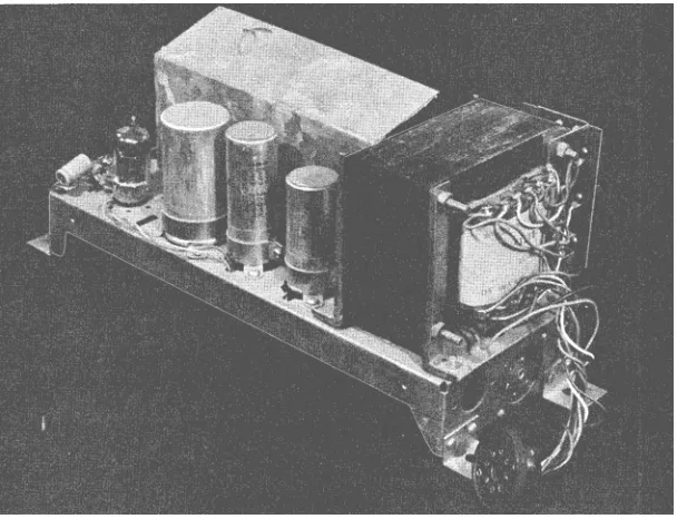
Vacuum tubes were found to have several built-in problems. Although the tubes were lightweight, associated components and chassis were quite heavy. It was not uncommon for such chassis to weigh 40 to 50 pounds. In addition, the tubes generated a lot of heat, required a warm-up time from 1 to 2 minutes, and required hefty power supply voltages of 300 volts dc and more.
No two tubes of the same type were exactly alike in output characteristics. Therefore, designers were required to produce circuits that could work with any tube of a particular type. This meant that additional components were often required to tune the circuit to the output characteristics required for the tube used.
[image:17.612.155.459.278.511.2]Figure 1-1 shows a typical vacuum-tube chassis. The actual size of the transformer is approximately 4 × 4 × 3 inches. Capacitors are approximately 1 × 3 inches. The components in the figure are very large when compared to modern microelectronics.
Figure 1-1.—Typical vacuum tube circuit.
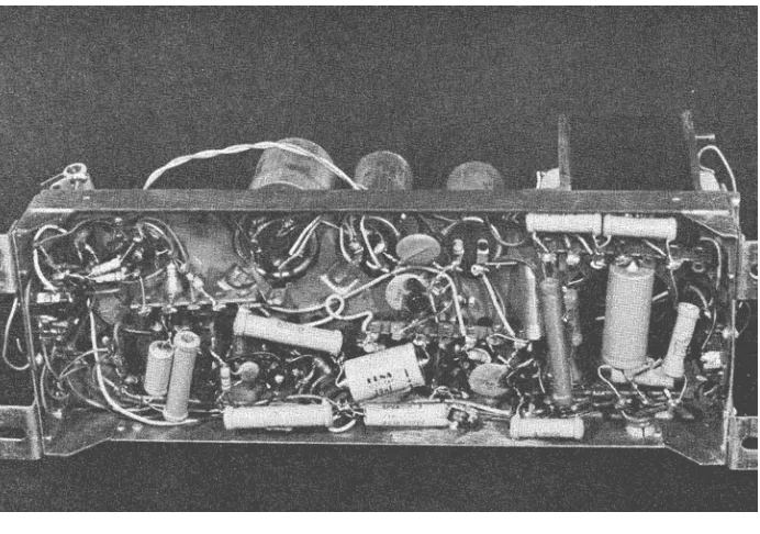
A circuit could be designed either as a complete system or as a functional part of a larger system. In complex systems, such as radar, many separate circuits were needed to accomplish the desired tasks. Multiple-function tubes, such as dual diodes, dual triodes, tetrodes, and others helped considerably to reduce the size of circuits. However, weight, heat, and power consumption continued to be problems that plagued designers.
Figure 1-2.—Point-to-point wiring.
Vacuum-tube circuits proved to be reliable under many conditions. Still, the drawbacks of large size, heavy weight, and significant power consumption made them undesirable in most situations. For
example, computer systems using tubes were extremely large and difficult to maintain. ENIAC, a completely electronic computer built in 1945, contained 18,000 tubes. It often required a full day just to locate and replace faulty tubes.
In some applications, we are still limited to vacuum tubes. Cathode-ray tubes used in radar, television, and oscilloscopes do not, as yet, have solid-state counterparts.
One concept that eased the technician's job was that of MODULAR PACKAGING. Instead of building a system on one large chassis, it was built of MODULES or blocks. Each module performed a necessary function of the system. Modules could easily be removed and replaced during troubleshooting and repair. For instance, a faulty power supply could be exchanged with a good one to keep the system operational. The faulty unit could then be repaired while out of the system. This is an example of how the module concept improved the efficiency of electronic systems. Even with these advantages, vacuum tube modules still had faults. Tubes and point-to-point wiring were still used and excessive size, weight, and power consumption remained as problems to be overcome.
Vacuum tubes were the basis for electronic technology for many years and some are still with us. Still, emphasis in vacuum-tube technology is rapidly becoming a thing of the past. The emphasis of technology is in the field of microelectronics.
Q4. What discovery proved to be the foundation for the development of the vacuum tube? Q5. Name the components which greatly increase the weight of vacuum-tube circuitry. Q6. What are the disadvantages of point-to-point wiring?
Q7. What is a major advantage of modular construction?
SOLID-STATE DEVICES
Now would be a good time for you to review the first few pages of NEETS, Module 7,Introduction to Solid-State Devices and Power Supplies, as a refresher for solid-state devices.
The transition from vacuum tubes to solid-state devices took place rapidly. As new types of transistors and diodes were created, they were adapted to circuits. The reductions in size, weight, and power use were impressive. Circuits that earlier weighed as much as 50 pounds were reduced in weight to just a few ounces by replacing bulky components with the much lighter solid-state devices.
The earliest solid-state circuits still relied on point-to-point wiring which caused many of the disadvantages mentioned earlier. A metal chassis, similar to the type used with tubes, was required to provide physical support for the components. The solid-state chassis was still considerably smaller and lighter than the older, tube chassis. Still greater improvements in component mounting methods were yet to come.
One of the most significant developments in circuit packaging has been the PRINTED CIRCUIT BOARD (pcb), as shown in figure 1-3. The pcb is usually an epoxy board on which the circuit leads have been added by the PHOTOETCHING process. This process is similar to photography in that copper-clad boards are exposed to controlled light in the desired circuit pattern and then etched to remove the
unwanted copper. This process leaves copper strips (LANDS) that are used to connect the components. In general, printed circuit boards eliminate both the heavy, metal chassis and the point-to-point wiring.
Figure 1-3.—Printed circuit board (pcb).
Although printed circuit boards represent a major improvement over tube technology, they are not without fault. For example, the number of components on each board is limited by the sizes and shapes of components. Also, while vacuum tubes are easily removed for testing or replacement, pcb components are soldered into place and are not as easily removed.
Another mounting form that has been used to increase the number of components in a given space is the CORDWOOD MODULE, shown in figure 1-4. You can see that the components are placed
perpendicular to the end plates. The components are packed very closely together, appearing to be stacked like cordwood for a fireplace. The end plates are usually small printed circuit boards, but may be
insulators and solid wire, as shown in the figure. Cordwood modules may or may not be
ENCAPSULATED (totally imbedded in solid material) but in either case they are difficult to repair.
Figure 1-4.—Cordwood module. Q9. List the major advantages of printed circuit boards.
Q10. What is the major disadvantage of printed circuit boards?
Q11. The ability to place more components in a given space is an advantage of the _______.
INTEGRATED CIRCUITS
Many advertisements for electronic equipment refer to integrated circuits or solid-state technology. You know the meaning of the term solid-state, but what is an INTEGRATED CIRCUIT? The accepted Navy definition for an integrated circuit is that it consists of elements inseparably associated and formed on or within a single SUBSTRATE (mounting surface). In other words, the circuit components and all interconnections are formed as a unit. You will be concerned with three types of integrated circuits: MONOLITHIC, FILM, and HYBRID.
FILM INTEGRATED CIRCUITS are broken down into two categories, THIN FILM and THICK FILM. Film components are made of either conductive or nonconductive material that is deposited in desired patterns on a ceramic or glass substrate. Film can only be used as passive circuit components, such as resistors and capacitors. Transistors and/or diodes are added to the substrate to complete the circuit. Differences in thin and thick film will be discussed later in this topic.
HYBRID INTEGRATED CIRCUITS combine two or more integrated circuit types or combine one or more integrated circuit types and DISCRETE (separate) components. Figure 1-5 is an example of a hybrid integrated circuit consisting of silicon chips and film circuitry. The two small squares are chips and the irregularly shaped gray areas are film components.
Figure 1-5.—Hybrid integrated circuit.
STATE-OF-THE-ART MICROELECTRONICS.
Microelectronic technology today includes thin film, thick film, hybrid, and integrated circuits and combinations of these. Such circuits are applied in DIGITAL, SWITCHING, and LINEAR (analog) circuits. Because of the current trend of producing a number of circuits on a single chip, you may look for further increases in the packaging density of electronic circuits. At the same time you may expect a reduction in the size, weight, and number of connections in individual systems. Improvements in reliability and system capability are also to be expected.
Thus, even as existing capabilities are being improved, new areas of microelectronic use are being explored. To predict where all this use of technology will lead is impossible. However, as the demand for increasingly effective electronic systems continues, improvements will continue to be made in state-of-the-art microelectronics to meet the demands.
used instead of one that has been separated into individual circuits. In lsi and vlsi, a variety of circuits can be implanted on a wafer resulting in further size and weight reduction. ICs in modern computers, such as home computers, may contain the entire memory and processing circuits on a single substrate.
Figure 1-6.—Large-scale integration device (lsi).
Large-scale integration is generally applied to integrated circuits consisting of from 1,000 to 2,000 logic gates or from 1,000 to 64,000 bits of memory. A logic gate, as you should recall from NEETS, Module 13,Introduction to Number Systems, Boolean Algebra, and Logic Circuits, is an electronic switching network consisting of combinations of transistors, diodes, and resistors. Very large-scale integration is used in integrated circuits containing over 2,000 logic gates or greater than 64,000 bits of memory.
Q12. Define integrated circuit.
Q13. What are the three major types of integrated circuits? Q14. How do monolithic ICs differ from film ICs?
Q15. What is a hybrid IC?
Q16. How many logic gates could be contained in lsi?
FABRICATION OF MICROELECTRONIC DEVICES
The purpose of this section is to give you a simplified overview of the manufacture of
Development of a microelectronic device begins with a demand from industry or as the result of research. A device that is needed by industry may be a simple diode network or a complex circuit consisting of thousands of components. No matter how complex the device, the basic steps of production are similar. Each type of device requires circuit design, component arrangement, preparation of a
substrate, and the depositing of proper materials on the substrate.
The first consideration in the development of a new device is to determine what the device is to accomplish. Once this has been decided, engineers can design the device. During the design phase, the engineers will determine the numbers and types of components and the interconnections, needed to complete the planned circuit.
COMPONENT ARRANGEMENT
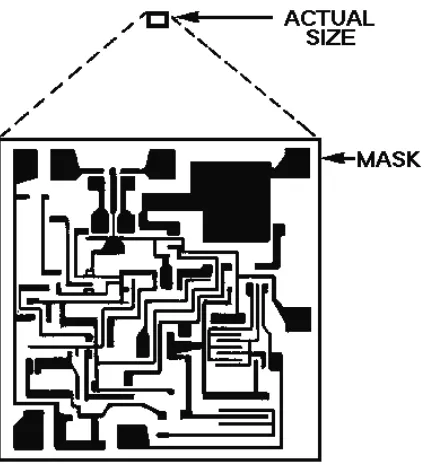
[image:23.612.204.419.415.652.2]Planning the component arrangement for a microelectronic device is a very critical phase of production. Care must be taken to ensure the most efficient use of space available. With simple devices, this can be accomplished by hand. In other words, the engineers can prepare drawings of component placement. However, a computer is used to prepare the layout for complex devices. The computer is able to store the characteristics of thousands of components and can provide a printout of the most efficient component placement. Component placement is then transferred to extremely large drawings. During this step, care is taken to maintain the patterns as they will appear on the substrate. Figure 1-7 shows a fairly simple IC MASK PATTERN. If this pattern were being prepared for production, it would be drawn several hundred times the size shown and then photographed. The photo would then be reduced in size until it was the actual desired size. At that time, the pattern would be used to produce several hundred patterns that would be used on one substrate. Figure 1-8 illustrates how the patterns would be distributed to act as a WAFER MASK for manufacturing.
Figure 1-8.—Wafer mask distribution.
A wafer mask is a device used to deposit materials on a substrate. It allows material to be deposited in certain areas, but not in others. By changing the pattern of the mask, we can change the component arrangement of the circuit. Several different masks may be used to produce a simple microelectronic device. When used in proper sequence, conductor, semiconductor, or insulator materials may be applied to the substrate to form transistors, resistors, capacitors, and interconnecting leads.
SUBSTRATE PRODUCTION
As was mentioned earlier in this topic, microelectronic devices are produced on a substrate. This substrate will be of either insulator or semiconductor material, depending on the type of device. Film and hybrid ICs are normally constructed on a glass or ceramic substrate. Ceramic is usually the preferred material because of its durability.
Substrates used in monolithic ICs are of semiconductor material, usually silicon. In this type of IC, the substrate can be an active part of the IC. Glass or ceramic substrates are used only to provide support for the components.
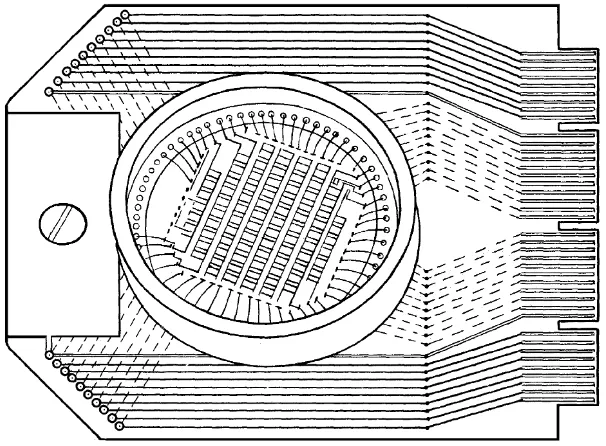
Semiconductor substrates are produced by ARTIFICIALLY GROWING cylindrical CRYSTALS of pure silicon or germanium. Crystals are "grown" on a SEED CRYSTAL from molten material by slowly lifting and cooling the material repeatedly. This process takes place under rigidly controlled atmospheric and temperature conditions.
Figure 1-9.—Crystal furnace.
The cylinder of semiconductor material that is grown is sliced into thicknesses of .010 to .020 inch in the first step of preparation, as shown in figure 1-10. These wafers are ground and polished to remove any irregularities and to provide the smoothest surface possible. Although both sides are polished, only the side that will receive the components must have a perfect finish.
Figure 1-10.—Silicon crystal and wafers.
Q17. What are the basic steps in manufacturing an IC?
Q18. Computer-aided layout is used to prepare _______ devices. Q19. What purpose do masks serve?
Q21. Describe the preparation of a silicon substrate.
FABRICATION OF IC DEVICES
Fabrication of monolithic ICs is the most complex aspect of microelectronic devices we will discuss. Therefore, in this introductory module, we will try to simplify this process as much as possible. Even though the discussion is very basic, the intent is still to increase your appreciation of the progress in microelectronics. You should, as a result of this discussion, come to realize that advances in manufacturing techniques are so rapid that staying abreast of them is extremely difficult.
Monolithic Fabrication.
Two types of monolithic fabrication will be discussed. These are the DIFFUSION METHOD and the EPITAXIAL METHOD.
DIFFUSION METHOD.—The DIFFUSION process begins with the highly polished silicon wafer being placed in an oven (figure 1-11). The oven contains a concentration impurity made up of impurity atoms which yield the desired electrical characteristics. The concentration of impurity atoms is diffused into the wafer and is controlled by controlling the temperature of the oven and the time that the silicon wafer is allowed to remain in the oven. This is called DOPING. When the wafer has been uniformly doped, the fabrication of semiconductor devices may begin. Several hundred circuits are produced simultaneously on the wafer.
Figure 1-11.—Wafers in a diffusion oven.
Figure 1-12.—Planar-diffused transistor.
1. An oxide coating is thermally grown over the n-type silicon starting material.
2. By means of the photolithographic process, a window is opened through the oxide layer. This is done through the use of masks, as discussed earlier.
3. The base of the transistor is formed by placing the wafer in a diffusion furnace containing a p-type impurity, such as boron. By controlling the temperature of the oven and the length of time that the wafer is in the oven, you can control the amount of boron diffused through the window (the boron will actually spread slightly beyond the window opening). A new oxide layer is then allowed to form over the area exposed by the window.
4. A new window, using a different mask much smaller than the first, is opened through the new oxide layer.
5. An n-type impurity, such as phosphorous, is diffused through the new window to form the emitter portion of the transistor. Again, the diffused material will spread slightly beyond the window opening. Still another oxide layer is then allowed to form over the window.
6. By means of precision-masking techniques, very small windows (about 0.005 inch in diameter) are opened in both the base and emitter regions of the transistor to provide access for electrical currents.
7. Aluminum is then deposited in these windows and alloyed to form the leads of the transistor or the IC.
EPITAXIAL METHOD.—The EPITAXIAL process involves depositing a very thin layer of silicon to form a uniformly doped crystalline region (epitaxial layer) on the substrate. Components are produced by diffusing appropriate materials into the epitaxial layer in the same way as the planar-diffusion method. When planar-planar-diffusion and epitaxial techniques are combined, the component
characteristics are improved because of the uniformity of doping in the epitaxial layer. A cross section of a typical planar-epitaxial transistor is shown in figure 1-13. Note that the component parts do not
penetrate the substrate as they did in the planar-diffused transistor.
Figure 1-13.—Planar-epitaxial transistor.
ISOLATION.—Because of the closeness of components in ICs, ISOLATION from each other becomes a very important factor. Isolation is the prevention of unwanted interaction or leakage between components. This leakage could cause improper operation of a circuit.
Techniques are being developed to improve isolation. The most prominent is the use of silicon oxide, which is an excellent insulator. Some manufacturers are experimenting with single-crystal silicon grown on an insulating substrate. Other processes are also used which are far too complex to go into here. With progress in isolation techniques, the reliability and efficiency of ICs will increase rapidly.
Thin Film
Thin film is the term used to describe a technique for depositing passive circuit elements on an insulating substrate with coating to a thickness of 0.0001 centimeter. Many methods of thin-film deposition exist, but two of the most widely used are VACUUM EVAPORATION and CATHODE SPUTTERING.
Figure 1-14.—Vacuum evaporation oven.
The wafers, with appropriate masks (figure 1-15), are placed above and at some distance from the material being evaporated. When the process is completed, the vacuum is released and the masks are removed from the wafers. This process leaves a thin, uniform film of the deposition material on all parts of the wafers exposed by the open portions of the mask. This process is also used to deposit
interconnections (leads) between components of an IC.
The vacuum evaporation technique is most suitable for deposition of highly reactive materials, such as aluminum, that are difficult to work with in air. The method is clean and allows a better contact between the layer of deposited material and the surface upon which it has been deposited. In addition, because evaporation beams travel in straight lines, very precise patterns may be produced.
CATHODE-SPUTTERING.—A typical cathode-sputtering system is illustrated in figure 1-16. This process is also performed in a vacuum. A potential of 2 to 5 kilovolts is applied between the anode and cathode (source material). This produces a GLOW DISCHARGE in the space between the electrodes. The rate at which atoms are SPUTTERED off the source material depends on the number of ions that strike it and the number of atoms ejected for each ion bombardment. The ejected atoms are deposited uniformly over all objects within the chamber. When the sputtering cycle is completed, the vacuum in the chamber is released and the wafers are removed. The masks are then removed from the wafers, leaving a deposit that forms the passive elements of the circuit, as shown in figure 1-17.
Figure 1-17.—Cathode-sputtering mask.
Finely polished glass, glazed ceramic, and oxidized silicon have been used as substrate materials for thin films. A number of materials, including nichrome, a compound of silicon oxide and chromium cermets, tantalum, and titanium, have been used for thin-film resistors. Nichrome is the most widely used.
The process for producing thin-film capacitors involves deposition of a bottom electrode, a
dielectric, and finally a top electrode. The most commonly used dielectric materials are silicon monoxide and silicon dioxide.
Thick Film
Thick films are produced by screening patterns of conducting and insulating materials on ceramic substrates. A thick film is a film of material with a thickness that is at least 10 times greater than the mean free path of an electron in that material, or approximately 0.001 centimeter. The technique is used to produce only passive elements, such as resistors and capacitors.
PROCEDURES.—One procedure used in fabricating a thick film is to produce a series of stencils called SCREENS. The screens are placed on the substrate and appropriate conducting or insulating materials are wiped across the screen. Once the conducting or insulating material has been applied, the screens are removed and the formulations are fired at temperatures above 600 degrees Celsius. This process forms alloys that are permanently bonded to the insulating substrate. To a limited extent, the characteristics of the film can be controlled by the firing temperature and length of firing time.
RESISTORS.—Thick-film resistance values can be held to a tolerance of ±10 percent. Closer tolerances are obtained by trimming each resistor after fabrication. Hundreds of different cermet
formulations are used to produce a wide range of component parameters. For example, the material used for a 10-ohm-per-square resistor is quite different from that used for a 100-kilohm-per-square resistor.
Hybrid Microcircuit
A hybrid microcircuit is one that is fabricated by combining two or more circuit types, such as film and semiconductor circuits, or a combination of one or more circuit types and discrete elements. The primary advantage of hybrid microcircuits is design flexibility; that is, hybrid microcircuits can be
designed to provide wide use in specialized applications, such as low-volume and high-frequency circuits. Several elements and circuits are available for hybrid applications. These include discrete
components that are electrically and mechanically compatible with ICs. Such components may be used to perform functions that are supplementary to those of ICs. They can be handled, tested, and assembled with essentially the same technology and tools. A hybrid IC showing an enlarged chip is shown in figure 1-18.
Figure 1-18.—Hybrid IC showing an enlarged chip.
Complete circuits are available in the form of UNCASED CHIPS (UNENCAPSULATED IC DICE). These chips are usually identical to those sold as part of the manufacturer's regular production line. They must be properly packaged and connected by the user if a high-quality final assembly is to be obtained. The circuits are usually sealed in a package to protect them from mechanical and environmental stresses. One-mil (0.001-inch), gold-wire leads are connected to the appropriate pins which are brought out of the package to allow external connections.
Q23. How do the two types of monolithic IC construction differ? Q24. What is isolation?
Q25. What methods are used to deposit thin-film components on a substrate? Q26. How are thick-film components produced?
Q27. What is a hybrid IC?
Q28. What is the primary advantage of hybrid circuits?
PACKAGING TECHNIQUES
Once the IC has been produced, it requires a housing that will protect it from damage. This damage could result from moisture, dirt, heat, radiation, or other sources. The housing protects the device and aids in its handling and connection into the system in which the IC is used. The three most common types of packages are the modified TRANSISTOR-OUTLINE (TO) PACKAGE, the FLAT PACK, and the DUAL INLINE PACKAGE (DIP).
Transitor-Outline Package
Transistor-Outline Package. The transistor-outline (TO) package was developed from early
Figure 1-19.—Exploded TO-5.
Figure 1-20.—TO-5 package.
Figure 1-21A.—TO-5 mounting PLUG-IN MOUNTING
Figure 1-21B.—TO-5 mounting EMBEDDED CAN(LEADS PLUGGED IN)
Flat Pack
Many types of IC flat packs are being produced in various sizes and materials. These packages are available in square, rectangular, oval, and circular configurations with 10 to 60 external leads. They may be
Figure 1-22.—Enlarged flat pack exploded view.
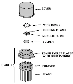
After the external leads are sealed to the mounting base, the rectangular area on the inside bottom of the base is treated with metal slurry to provide a surface suitable for bonding the monolithic die to the base. The lead and the metalized area in the bottom of the package are plated with gold. The die is then attached by gold-silicon bonding.
The die-bonding step is followed by bonding gold or aluminum wires between the bonding islands on the IC die and on the inner portions of the package leads. Next, a glass-soldered preformed frame is placed on top of the mounting base. One surface of the ceramic cover is coated with Pyroceram glass, and the cover is placed on top of the mounting base. The entire assembly is placed in an oven at 450 degrees Celsius. This causes the glass solder and Pyroceram to fuse and seal the cover to the mounting base. A ceramic flat pack is shown in figure 1-23. It has been opened so that you can see the chip and bonding wires.
Dual Inline Package
The dual inline package (DIP) was designed primarily to overcome the difficulties associated with handling and inserting packages into mounting boards. DIPs are easily inserted by hand or machine and require no spreaders, spacers, insulators, or lead-forming tools. Standard hand tools and soldering irons can be used to field-service the devices. Plastic DIPs are finding wide use in commercial applications, and a number of military systems are incorporating ceramic DIPS.
The progressive stages in the assembly of a ceramic DIP are illustrated in figure 1-24, views (A) through (E). The integrated-circuit die is sandwiched between the two ceramic elements, as shown in view (A). The element on the left of view (A) is the bottom half of the sandwich and will hold the integrated-circuit die. The ceramic section on the right is the top of the sandwich. The large well in view (B) protects the IC die from mechanical stress during sealing operations. Each of the ceramic elements is coated with glass which has a low melting temperature for subsequent joining and sealing. View (B) shows the Kovar lead frame stamped and bent into its final shape. The excess material is intended to preserve pin alignment. The holes at each end are for the keying jig used in the final sealing operation. The lower half of the ceramic package is inserted into the lead frame shown in view (C). The die is mounted in the well and leads are attached. The top ceramic elements are bonded to the bottom element shown in view (D) and the excess material is removed from the package. View (E) is the final product.
Figure 1-24.—DIP packaging steps.
used to encapsulate the IC die, no void will exist between the cover and die, as is the case with ceramic packaging.
At present, ceramic DIPs are the most common of the two package types to be found in Navy microelectronic systems. Figure 1-25 shows a DIP which has been opened.
Figure 1-25.—Dual inline package (DIP).
RECENT DEVELOPMENTS IN PACKAGING
Considerable effort has been devoted to eliminating the fine wires used to connect ICs to Kovar leads. The omission of these wires reduces the cost of integrated circuits by eliminating the costs associated with the bonding process. Further, omission of the wires improves reliability by eliminating a common cause of circuit failure.
A promising packaging technique is the face-down (FLIP-CHIP) mounting method by which conductive patterns are evaporated inside the package before the die is attached. These patterns connect the external leads to bonding pads on the inside surface of the die. The pads are then bonded to
appropriate pedestals on the package that correspond to those of the bonding pads on the die (figure 1-26).
Figure 1-26.—Flip-chip package.
wafer, as shown in figure 1-27. This type of structure imposes no electrical difficulty, and parasitic capacitance (under 0.05 picofarad per lead) is equivalent to that of a wire-bonded and brazed-chip assembly. In addition, the electrodes may be tapered to allow for lower inductance, impedance matching, and better heat conductance. The beam-lead technique is easily accomplished and does not have the disadvantages of chip brazing and wire bonding. The feasibility of this technique has been demonstrated in a variety of digital, linear, and thin-film circuits.
Figure 1-27.—Beam-lead technique.
Another advance in packaging is that of increasing the size of DIPs. General purpose DIPs have from 4 to 16 pins. Because of lsi and vlsi, manufacturers are producing DIPs with up to 64 pins. Although size is increased considerably, all the advantages of the DIP are retained. DIPs are normally designed to a particular specification set by the user.
Q29. What is the purpose of the IC package?
Q30. What are the three most common types of packages?
Q31. What two methods of manufacture are being used to eliminate bonding wires?
EQUIVALENT CIRCUITS
At the beginning of this topic, we discussed many applications of microelectronics. You should understand that these applications cover all areas of modern electronics technology. Microelectronic ICs are produced that can be used in many of these varying circuit applications to satisfy the needs of modern technology. This section will introduce you to some of these applications and will show you some
EQUIVALENT CIRCUIT comparisons of discrete components and integrated circuits.
J-K FLIP-FLOP AND IC SIZES
You should recall from NEETS, Module 13, Introduction to Number Systems, Boolean Algebra, and Logic Circuits, that a basic flip-flop is a device having two stable states and two input terminals (or types of input signals), each of which corresponds to one of the two states. The flip-flop remains in one state until caused to change to the other state by application of an input voltage pulse.
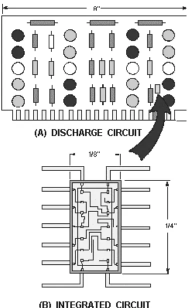
[image:40.612.146.458.290.501.2]A J-K flip-flop differs from the basic flip-flop because it has a third input terminal. A clock pulse, or trigger, is usually applied to this input to ensure proper timing in the circuit. An input signal must occur at the same time as the clock pulse to change the state of the flip-flop. The conventional J-K flip-flop circuit in figure 1-28 requires approximately 40 discrete components, 200 connections, and 300 processing operations. Each of these 300 operations (seals and connections) represents a possible source of failure. If all the elements of this circuit are integrated into one chip of silicon, the number of connections drops to approximately 14. This is because all circuit elements are intraconnected inside the package and the 300 processing operations are reduced to approximately 30. Figure 1-29 represents a size comparison of a discrete J-K circuit and an integrated circuit of the same type.
Figure 1-29.—J-K flip-flop discrete component and an IC.
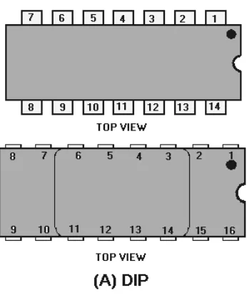
IC PACKAGE LEAD IDENTIFICATION (NUMBERING)
Figure 1-30A.—DIP and flat-pack lead numbering. DIP
Figure 1-30B.—DIP and flat-pack lead numbering. Flat-Pack
[image:42.612.229.389.351.548.2]Figure 1-31.—Lead numbering for a TO-5.
IC IDENTIFICATION
As mentioned earlier, integrated circuits are designed and manufactured for hundreds of different uses. Logic circuits, clock circuits, amplifiers, television games, transmitters, receivers, and musical instruments are just a few of these applications.
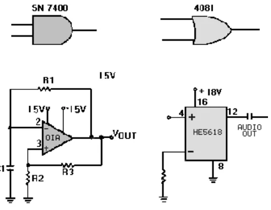
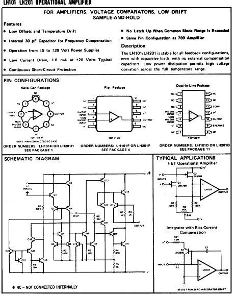
In schematic drawings, ICs are usually represented by one of the schematic symbols shown in figure 1-32. The IC is identified according to its use by the numbers printed on or near the symbol. That series of numbers and letters is also stamped on the case of the device and can be used along with the data sheet, as shown in the data sheet in figure 1-33, by circuit designers and maintenance personnel. This data sheet is provided by the manufacturer. It provides a schematic diagram and describes the type of device, its electrical characteristics, and typical applications. The data sheet may also show the pin configurations with all pins labeled. If the pin configurations are not shown, there may be a schematic diagram showing pin functions. Some data sheets give both pin configurations and schematic diagrams, as shown in figure 1-34. This figure illustrates a manufacturer's data sheet with all of the pin functions shown.
Q32. On DIP and flat-pack ICs viewed from the top, pin 1 is located on which side of the reference mark?
Q33. DIP and flat-pack pins are numbered consecutively in what direction? Q34. DIP and flat-pack pins are numbered consecutively in what direction? Q35. Viewed from the bottom, TO-5 pins are counted in what direction? Q36. The numbers and letters on ICs and schematics serve what purpose?
MICROELECTRONIC SYSTEM DESIGN CONCEPTS
You should understand the terminology used in microelectronics to become an effective and knowledgeable technician. You should be familiar with packaging concepts from a maintenance
standpoint and be able to recognize the different types of assemblies. You should also know the electrical and environmental factors that can affect microelectronic circuits. In the next section of this topic we will define and discuss each of these areas.
TERMINOLOGY
As in any special electronics field, microelectronics terms and definitions are used to clarify communications. This is done so that everyone involved in microelectronics work has the same knowledge of the field. You can imagine how much trouble you would have remembering 10 or more different names and definitions for a resistor. If standardization didn't exist for the new terminology, you would have far more trouble understanding microelectronics. To standardize terminology in
microelectronics, the Navy has adopted several definitions with which you should become familiar. These definitions will be presented in this section.
Microelectronics
Microelectronics is that area of electronics technology associated with electronics systems built from extremely small electronic parts or elements. Most of today's computers, weapons systems, navigation systems, communications systems, and radar systems make extensive use of microelectronics technology.
Microcircuit
A microcircuit is not what the time technician would recognize as an electronic circuit. The old-timer would no longer see the familiar discrete parts (individual resistors, capacitors, inductors,
transistors, and so forth). Microelectronic circuits, as discussed earlier, are complete circuits mounted on a substrate (integrated circuit). The process of fabricating microelectronic circuits is essentially one of building discrete component characteristics either into or onto a single substrate. This is far different from soldering resistors, capacitors, transistors, inductors, and other discrete components into place with wires and lugs. The component characteristics built into microcircuits are referred to as ELEMENTS rather than discrete components. Microcircuits have a high number of these elements per substrate compared to a circuit with discrete components of the same relative size. As a matter of fact, microelectronic circuits often contain thousands of times the number of discrete components. The term HIGH EQUIVALENT CIRCUIT DENSITY is a description of this element-to-discrete part relationship. For example, suppose you have a circuit with 1,000 discrete components mounted on a chassis which is 8 × 10 × 2 inches. The equivalent circuit in microelectronics might be built into or onto a single substrate which is only 3/8 × 1 ×
comparison to the distance between discrete components mounted on the large chassis. The elements within the substrate are interconnected on the single substrate itself to perform an electronic function. A microcircuit does not have any discrete components mounted on it as do printed circuit boards, circuit card assemblies, and modules composed exclusively of discrete component parts.
Microcircuit Module
Microcircuits may be used in combination with discrete components. An assembly of microcircuits or a combination of microcircuits and discrete conventional electronic components that performs one or more distinct functions is a microcircuit module. The module is constructed as an independently
[image:47.612.210.403.251.397.2]packaged, replaceable unit. Examples of microcircuit modules are printed circuit boards and circuit card assemblies. Figure 1-35 is a photograph of a typical microcircuit module.
Figure 1-35.—Microcircuit module.
Miniature Electronics
Miniature electronics includes miniature electronic components and packages. Some examples are printed circuit boards, printed wiring boards, circuit card assemblies, and modules composed exclusively
of discrete electronic parts and components (excluding microelectronic packages) mounted on boards, assemblies, or modules. MOTHER BOARDS, large printed circuit boards with plug-in modules, are considered miniature electronics. Cordwood modules also fall into this category. Miniature motors, synchros, switches, relays, timers, and so forth, are also classified as miniature electronics.
Recall that microelectronic components contain integrated circuits. Miniature electronics contain discrete elements or parts. You will notice that printed circuit boards and circuit card assemblies are mentioned in more than one definition. To identify the class (microminiature or miniature) of the unit, you must first determine the types of components used.
Q37. Standardized terms improve what action between individuals?
Q38. Microcircuit refers to any component containing what types of elements?
Q39. Components made up exclusively of discrete elements are classified as what type of electronics?
SYSTEM PACKAGING
account all environmental and electrical factors that may affect the system. This includes temperature, humidity, vibration, and electrical interference. The design factor that has the greatest impact on you, as the technician, is the MAINTAINABILITY of the system. The designer must take into account how well you will be able to locate problems, identify the faulty components, and make the necessary repairs. If a system cannot be maintained easily, then it is not an efficient system. PACKAGING, the method of enclosing and mounting components, is of primary importance in system maintainability.
Levels of Packaging
[image:48.612.192.419.246.555.2]For the benefit of the technician, system packaging is usually broken down to five levels (0 to IV). These levels are shown in figure 1-36.
Figure 1-36.—Packaging levels.
LEVEL 0.—Level 0 packaging identifies nonrepairable parts, such as integrated circuits, transistors, resistors, and so forth. This is the lowest level at which you can perform maintenance. You are limited to simply replacing the faulty element or part. Depending on the type of part, repair might be as simple as plugging in a new relay. If the faulty part is an IC, special training and equipment will be required to accomplish the repair. This will be discussed in topic 2.
maintenance you can replace the faulty module with a good one. The faulty module can then be repaired at a later time or discarded. This concept significantly reduces the time equipment is inoperable.
Figure 1-37.—Printed circuit board (pcb).
LEVEL II.—Level II packaging is composed of large printed circuit boards and/or cards (mother boards). Typical units of this level are shown in figures 1-37 and 1-38. In figure 1-38 the card measures 15 × 5.25 inches. The large dual inline packages (DIPs) are 2.25 inches x 0.75 inch. Other DIPs on the pcb are much smaller. Interconnections are shown between DIPs. You should also be able to locate a few discrete components. Repair consists of removing the faulty DIP or discrete component from the pcb and replacing it with a new part. Then the pcb is placed back into service. The removed part may be a level 0 or I part and would be handled as described in those sections. In some cases, the entire pcb should be replaced.
[image:49.612.235.377.482.670.2]LEVEL III.—Drawers or pull-out chassis are level III units, as shown in figure 1-36. These are designed for accessibility and ease of maintenance. Normally, circuit cards associated with a particular subsystem will be grouped together in a drawer. This not only makes for an orderly arrangement of subsystems but also eliminates many long wiring harnesses. Defective cards are removed from such drawers and defective components are repaired as described in level II.
LEVEL IV.—Level IV is the highest level of packaging. It includes the cabinets, racks, and wiring harnesses necessary to interconnect all of the other levels. Other pieces of equipment of the same system classified as level IV, such as radar antennas, are broken down into levels 0 to III in the same manner.
During component troubleshooting procedures, you progress from level IV to III to II and on to level 0 where you identify the faulty component. As you become more familiar with a system, you should be able to go right to the drawer or module causing the problem.
Q40. Resistors, capacitors, transistors, and the like, are what level of packaging? Q41. Modules or submodules attached to a mother board are what packaging level? Q42. What is the packaging level of a pcb?
INTERCONNECTIONS IN PRINTED CIRCUIT BOARDS
As electronic systems become more complex, interconnections between components also becomes more complex. As more components are added to a given space, the requirements for interconnections become extremely complicated. The selection of conductor materials, insulator materials, and component physical size can greatly affect the performance of the circuit. Poor choices of these materials can
contribute to poor signals, circuit noise, and unwanted electrical interaction between components. The three most common methods of interconnection are the conventional pcb, the multilayer pcb, and the modular assembly. Each of these will be discussed in the following sections.
Conventional Printed Circuit Board
Printed circuit boards were discussed earlier in topic 1. You should recall that a conventional pcb consists of glass-epoxy insulating base on which the interconnecting pattern has been etched. The board may be single- or double-sided, depending on the number of components mounted on it. Figures 1-37 and 1-38 are examples of conventional printed circuit boards.
Multilayer Printed Circuit Board.
The multilayer printed circuit board is emerging as the solution is interconnection problems associated with high-density packaging. Multilayer boards are used to:
•
reduce weight•
conserve space in interconnecting circuit modules•
eliminate costly and complicated wiring harnesses•
provide shielding for a large number of conductors•
allow greater wiring density on boardsFigure 1-39 illustrates how individual boards are mated to form the multilayer unit. Although all multilayer boards are similarly constructed, various methods can be used to interconnect the circuitry from layer to layer. Three proven processes are the clearance-hole, plated-through hole, and layer build-up methods.
Figure 1-39.—Multilayer pcb.
CLEARANCE-HOLE METHOD.—In the CLEARANCE-HOLE method, a hole is drilled in the copper island (terminating end) of the appropriate conductor on the top layer. This provides access to a conductor on the second layer as shown by hole A in figure 1-40. The clearance hole is filled with solder to complete the connection. Usually, the hole is drilled through the entire assembly at the connection site. This small hole is necessary for the SOLDER-FLOW PROCESS used with this interconnection method.
Conductors located several layers below the top are connected by using a STEPPED-DOWN HOLE PROCESS. Before assembly of a three-level board, a clearance hole is drilled down to the first layer to be interconnected. The first layer to be interconnected is predrilled with a hole smaller than those drilled in layers 1 and 2; succeeding layers to be connected have progressively smaller clearance holes. After assembly, the exposed portion of the conductors are interconnected by filling the stepped-down holes with solder, as shown by hole B in figure 1-40. The larger the number of interconnections required at one point, the larger must be the diameter of the clearance holes on the top layer. Large clearance holes on the top layer allow less space for components and reduce packaging density.
PLATED-THROUGH-HOLE METHOD.—The PLATED-THROUGH-HOLE method of interconnecting conductors is illustrated in figure 1-41. The first step is to temporarily assemble all the layers into their final form. Holes corresponding to required connections are drilled through the entire assembly and then the unit is disassembled. The internal walls of those holes to be interconnected are plated with metal which is 0.001 inch thick. This, in effect, connects the conductor on the board surface through the hole itself. This process is identical to that used for standard printed circuit boards. The boards are then reassembled and permanently bonded together with heat and pressure. All the holes are plated through with metal.
Figure 1-41.—Plated through-hole interconnection.
LAYER BUILD-UP METHOD.—With the LAYER BUILD-UP method, conductors and insulation layers are alternately deposited on a backing material, as shown in figure 1-42. This method produces copper interconnections between layers and minimizes the thermal expansion effects of
Figure 1-42.—Layer build-up technique.
Advantages and Disadvantages of Printed Circuit Boards
Some of the advantages and disadvantages of printed circuit boards were discussed earlier in this topic. They are strong, lightweight, and eliminate point-to-point wiring. Multilayer printed circuit boards allow more components per card. Entire circuits or even subsystems may be placed on the same card. However, these cards do have some drawbacks. For example, all components are wired into place, repair of cards requires special training and/or special equipment, and some cards cannot be economically repaired because of their complexity (these are referred to as THROWAWAYS).
MODULAR ASSEMBLIES
Figure 1-43A.—Evolution of modular assemblies. CORDWOOD.
Figure 1-43C.—Evolution of modular assemblies. INTEGRATED-CIRCUIT.
Cordwood Modules.
The cordwood assembly, shown in view (A) of figure 1-43, was designed and fabricated in various forms and sizes, depending on user requirements. This design was used to reduce the physical size and increase the component density and complexity of circuits through the use of discrete devices. However, the use of the technique was somewhat limited by the size of available discrete components used.
Micromodules
The next generation assembly was the micromodule. Designers tried to achieve maximum density in this design by using discrete components, thick- and thin-film technologies, and the insulator substrate principle. The method used in this construction technique allowed for the efficient use of space and also provided the mechanical strength necessary to withstand shock and vibration.
Semiconductor technology was then improved further with the introduction of the integrated circuit. The flat-pack IC form, shown in view (C), emphasizes the density and complexity that exists with this technique. This technology provides the means of reducing the size of circuits. It also allows the reduction of the size of systems through the advent of the lsi circuits that are now available and vlsi circuits that are being developed by various IC manufacturers.
Continuation of this trend toward microminiaturization will result in system forms that will require maintenance personnel to be specially trained in maintenance techniques to perform testing, fault isolation, and repair of systems containing complex miniature and microminiature circuits.
Q43. What are the three most common methods of interconnections?
Q44. Name the three methods of interconnecting components in multilayer printed circuit boards. Q45. What is one of the major disadvantages of multilayer printed circuit boards?
ENVIRONMENTAL CONSIDERATIONS
The environmental requirements of each system design are defined in the PROCUREMENT SPECIFICATION. Typical environmental requirements for an IC, for example, are shown in table 1-1. After these system requirements have been established, components, applications, and packagi