i
FROM VAN DER WAALS TO COULOMBIC HETEROSTRUCTURES: UNDERSTANDING CHARGE TRANSFER IN 2D MATERIALS
Adam Haas Woomer
A dissertation submitted to the faculty at the University of North Carolina at Chapel Hill in partial fulfillment of the requirements for the degree of Doctor of Philosophy in the Department
of Chemistry.
Chapel Hill 2018
Approved by: Scott C. Warren James F. Cahoon Wei You
iii ABSTRACT
Adam Haas Woomer: From van der Waals to Coulombic Heterostructures: Understanding Charge Transfer in 2D Materials
(Under the direction of Scott C. Warren)
Innovations in semiconductor technologies, such as transistors, photovoltaics, and light-emitting diodes, require materials with highly designed properties. Zero-dimensional quantum dots and one-dimensional conjugated polymers are ideal building blocks for engineered three-dimensional materials because of their size-dependent quantum-confined optoelectronic
properties, however, two-dimensional materials have been largely unexplored. Here I show that reassembled films of 2D semiconductors retain their quantum-confined properties due to
turbostratic disorder and interlayer contaminants, yet are still electrically conductive. I designed uniaxially pressure and temperature-dependent van der Pauw conductivity measurements to determine that charge transport proceeds via hopping, with an activation energy expected for nanoparticle systems. In this manner, we can design 3D materials with virtually any
optoelectronic propertie with the appropriate choice of 2D material and thickness.
iv
covalent bonds, Coloumbic heterostructures fall within the van der Waals gap, a largely
unexplored region of materials. I then highlight the exciting new properties that can result from the assembly of Coulombic heterostructures, including superlubricity, defect free doping,
v
vi
ACKNOWLEDGEMENTS
First, I would like to thank Professor Scott Warren for his guidance and support during my time in his laboratory. He has been a role model for the kind scientist I would like to be as I move forward in my career, and has taught me to think critically and question everything.
I would also like to thank Dan Druffel and Tyler Farnsworth, who I worked the closest with during this journey. Your stimulating discussions, aid with experiments, and coffee trips have kept me motivated and excited about our research. I am looking forward to reading about the contributions to science that each of you will produce in the future. After all of our
experiences together, I can confidently say that your future colleagues and collaborators will be lucky to be working with such great scientists.
I am so proud to have been a member of the Warren lab, and I couldn’t have imagined a greater group to have been a part of. From cake making parties to board games to eating out on Franklin Street, thank you to everyone for making graduate school a little less stressful and for putting up with my shenanigans along the way. I hope that I have been able to make you smile, laugh, or even feel a little less overwhelmed, as you have done for me every day.
I would also like thank to my wife, Claire, who has continued to believe in me,
vii
TABLE OF CONTENTS
LIST OF TABLES ... x
LIST OF FIGURES ... xi
LIST OF ABBREVIATIONS ... xiii
CHAPTER ONE – INTRODUCTION ... 1
1.1 Engineered 3D materials with quantum confined properties ... 1
1.2 2D Materials as building blocks ... 2
1.2.1 Weak interlayer interactions in 2DM architectures: van der Waals forces... 4
1.2.2 Strong interactions in 2DM architectures: bonding and charge transfer ... 5
1.3 Research Overview ... 6
REFERENCES ... 8
CHAPTER TWO – METHODS FOR PREPARATION, PROCESSING, AND CHARACTERIZATION OF 2D MATERIALS AND FILMS ... 15
2.1 Introduction ... 15
2.2 Preparation of 2D materials from bulk layered crystals ... 15
2.2.1 Mechanical Exfoliation ... 15
2.2.2 Liquid Exfoliation ... 16
2.3 Advanced transmission electron microscopy techniques for 2D materials ... 19
2.3.1 Edge contrast analysis ... 19
2.3.2 Electron diffraction and Fast-Fourier transforms (FFTs) to determine material thickness... 24
viii
2.4.1 Van der Pauw geometry for conductivity and activation energy ... 28
2.4.2 Preparation of vacuum filtered films ... 30
2.4.3 Preparation of LB trough films, post-deposition ... 31
2.4.4 Electrical measurements on 2DM films with pressure and temperature control ... 32
2.5 Application of DFT for 2D materials ... 34
2.5.1 General methods using CASTEP ... 35
2.5.2 Grimme’s DFT-D correction for dispersion forces... 36
2.5.3 Binding energy, gravitational deformation and phonon modes for 2DM stability... 37
2.5.4 Self-interaction error and hybrid exchange functionals for accurate band gap determination of 2DMs ... 40
2.5.5 Bader charge transfer in 2DM systems ... 41
REFERENCES ... 43
CHAPTER THREE – PHOSPHORENE: SYNTHESIS, CHARACTERIZATION, AND QUANTITATIVE OPTICAL SPECTROSCOPY ... 48
3.1 Introduction ... 48
3.2 Liquid exfoliation of black phosphorus ... 50
3.3 Characterization of 2D phosphorus ... 53
3.4 Exfoliation of black phosphorus at the 10-gram scale ... 59
3.5 Optical absorption in 2D phosphorus: background ... 61
3.6 Optical absorption in 2D phosphorus: measurement and Tauc analysis ... 66
3.7 A method for determining absorption edges in quantum-confined semiconductors ... 69
3.8 Thickness-dependent absorption edges of black and 2D phosphorus ... 74
ix
REFERENCES ... 82
CHAPTER FOUR – ENGINEERED 3D MATERIALS WITH QUANTUM-CONFINED 2D PROPERTIES ... 89
4.1 Introduction ... 89
4.2 Qualitative optical evidence of quantum confinement in 2DM films... 91
4.3 Structural investigations of 2DM films... 92
4.4 Van der Pauw Conductivity Measurements and Activation Energy of 2DM Films ... 94
4.5 Raman and Photoluminescence evidence of Quantum confinement ... 96
REFERENCES ... 101
CHAPTER FIVE – BEYOND VAN DER WAALS FORCES: MASSIVE CHARGE TRANSFER AND QUASI-BOND FORMATION IN COULOMBIC HETEROSTRUCTURES ... 105
5.1 Introduction ... 105
5.2 Interlayer Distance and Charge Transfer in Coulombic Heterostructures ... 107
5.3 Binding Energy and Orbital Projections in Coulombic Heterostrucutres ... 110
5.4 Quasi-bonding interactions in Coulombic Heterostructures ... 114
5.5 Unexpected properties of Coulombic Heterostructures ... 118
5.6 Conclusions ... 120
REFERENCES ... 121
x
LIST OF TABLES
Table 2-1. Labeling of centrifugation fractions containing 2DM suspensions ... 18 Table 3-1. Reported optical, mobility, and band gaps of 2D phosphorus: ... 62 Table 3-2. Electronic band-to-band transitions in 2D phosphorus ... 77 Table A1-1: Summary of optimized heterostructure lattice constants
and interlayer distance. ... 124 Table A1-2: Bader analysis results for Coulombic Heterostructures ... 125
xi
LIST OF FIGURES
Figure 1-1. Layered van der Waals solids for 2D Materials ... 2
Figure 2-1. Electron Microscope Optics and Design ... 19
Figure 2-2. Common van der Pauw resistivity measurement geometries ... 29
Figure 2-3. 2DM Films with electrical contacts ... 31
Figure 2-4. Uniaxial pressure and temperature controlled conductivity measurements ... 32
Figure 3-1. Liquid exfoliation of black phosphorus ... 51
Figure 3-2. Survey of organic liquids for liquid exfoliation of black phosphorus ... 52
Figure 3-3. TEM characterization of liquid-exfoliated 2D phosphorus ... 54
Figure 3-4. Centrifugation rate to control thickness and lateral size ... 56
Figure 3-5. Oxidation studies of Black Phosphorus ... 58
Figure 3-6. Scaled-up production of 2D phosphorus ... 60
Figure 3-7. UV-vis-nIR spectroscopy of black phosphorus and few-layer flakes ... 68
Figure 3-8. “Alpha method” for band gap determination ... 70
Figure 3-9. Experimentally determined band gap (low energy) and high-energy transitions of 2D and bulk black phosphorus ... 76
Figure 4-1. Suspensions and films of 2DM exhibiting quantum confined optical properties and electronic coupling ... 92
Figure 4-2. Structural analysis of MoS2 films: ... 94
Figure 4-3. Electrical properties of MoS2 films with varying flake thickness ... 96
Figure 4-4. Quantum confinement of 2D material films ... 99
Figure 5-1. Achieving high degrees of charge transfer by combining 2D electrenes with other 2D materials ... 108
Figure 5-2. Bonding and charge transfer in Molecular compounds, van der Waals materials, and Coulombic heterostructures ... 109
xii
Figure 5-4. Electron Density Difference of Different Bonding for
Coulombic Heterostructures and vdW, Ionic, and Covalent compounds ... 115
Figure 5-5. Donor-acceptor analogy to rationalize charge transfer in hBN case ... 116
Figure 5-6. Work function tailoring, superlubricity and Li ion intercalation of Coulombic Heterostructures ... 119
Figure A1-1. Coulombic heterostructures studied by DFT ... 124
Figure A1-2. Band Structure, DOS, and Orbital projections around Fermi Level for CH ... 125
Figure A1-3. Bond length analysis for all crystalline solids ... 126
xiii
LIST OF ABBREVIATIONS
1D One-dimensional
2D Two-dimensional
2DM(s) Two-dimensional Material(s)
3D Three dimensional
AFM Atomic force microscopy
BFGS Broyden-Fletcher-Goldfarb-Shanno CASTEP Cambridge Serial Total Energy Package
CCD Charge-coupled device
CVD Chemical Vapor Deposition
DFT Density Functional Theory
DFT-D Density Functional Theory with Dispersion forces DMPU 1,3-dimethyl-3,4,5,6-tetrahydro-2(1H)-pyrimidinone
DP Diffraction pattern
e-BN electrene-boron nitride heterostructure e-C electrene-graphene heterostructure e-P electrene-phosphorene heterostructure e-ZrS2 electrene-zirconium disulfide heterostructure
EBE Exciton binding energy
EDD Electron density difference
EDFT Ensemble density functional theory FETT Field effect tunneling transistor
xiv FT-IR Fourier transform-infrared
GGA Generalized-gradient approximation
hBN hexagonal Boron Nitride
HF Hartree-fock
HRTEM high-resolution transmission electron microscopy
HSE Heyd-Scuseria-Ernzerhof
ICP-MS Inductively coupled plasma-mass spectroscopy
IPA Isopropanol
JEMS Java electron microscopy simulation
LB Langmuir-Blodgett
LDA Local density approximation
nBuLi n-butyllithium
NMP N-methyl-2-pyrrolidone
PBE Perdew-Burke-Ernzerhof
PL Photoluminescence
PTFE Polytetrafluoroethylene PVDF Polyvinylidene Fluoride RCF Rotational centrifugal force
RPM Rotations per minute
SDC Small digital controller
xv TMD Transition Metal Dichalcogenides UV-vis-nIR Ultraviolet-visible-near infrared
vdP van der Pauw
vdW van der Waals
VF Vacuum filtered
XPS X-ray photoelectron spectroscopy
1
CHAPTER ONE – INTRODUCTION 1.1 Engineered 3D materials with quantum confined properties
Thin and thick films with tunable optoelectronic properties are essential for the design of many technologies, including photovoltaics, transistors, and light emitting diodes. As such, there have been investigations into designing three-dimensional materials from zero-dimensional and one-dimensional building blocks, that retain their highly tunable quantum-confined properties. Quantum dots1 have attracted broad interest because of their size-dependent electronic structure and controllable physical properties2-5. Colloidal quantum dots can be deposited from solution as films6-7 that retain their quantum-confined optical properties despite electronic coupling and effective charge transport between nanoparticles8-10. These materials have been described as ‘confined-yet-coupled’ systems, in which the electrical transport properties and optical properties can be finely tuned with nanoparticle size and ligand length. Long ligands result in low
2 1.2 2D Materials as building blocks
Two-dimensional materials (2DM) have emerged as an important class of nanomaterials with applications in energy conversion14 and information technology15-16. Individual 2D flakes can function as building blocks for engineered 3D materials, and often possess unique optical, electrical, and physical properties due to quantum confinement. As the first exfoliated 2DM, graphene has been shown to have a high carrier mobility of 100,000 cm2 V-1 s-1, yet has low optical absorption and is a quasi-metal with no band gap17. While the lack of band gap has limited some of the applications of graphene, 2D transition metal dichalcogenides (TMDs) such as molybdenum disulfide (MoS2) and tungsten diselenide (WSe2) offered new alternatives to designing semiconducting materials. MoS2 has a thickness dependent band gap that transitions from 1.2 to 1.8 eV as the materially is thinned, and is direct in the completely quantum confined case of a single layer18. The isoelectric equivalent of graphene, 2D hexagonal boron nitride (hBN), is an insulator with a band gap of 5.9 eV.
3
Graphene, hBN, and the transition metal dichalcogenides (TMDs) span a large range of optoelectronic properties and can be thought of as the iconic pillars for designing 2DM
architectures. Applications in spintronics, photovoltaics, and transistors, however, require materials with increasingly specific magnetic, optical, and electronic properties. Appropriately, the library of 2DMs is constantly expanding from both experimental observation and
computational prediction to meet these needs. Elemental 2DMs beyond graphene now include silicene19-21, phosphorene22-23, antimonene24-25, arsenene25, and borophene26-27, which possess quantum-confined optical properties or topological Dirac states. Ferromagnetic layered
materials, such as Cr2Ge2Te628-29 and Gd2C30, and their exfoliation to monolayers would push the field of 2DM nanoelectronics into advanced magnetic and spintronic applications. One of the most interesting new additions to the 2DM family are the electrenes. Prepared from the exfoliation of layered electrides, the electrenes consist of [M2X]+ ionic slabs and an anionic electron gas occupying the interlayer space to maintain charge neutrality31-32. Electrenes can be prepared from pnictogenides (X=N, P M= Ca, Sr, Ba) and carbides (X=C, M=Y, Gd, Sc, Ho) and offer an opportunity for fundamental investigations of interlayer interactions in 2DM
heterostructures.
4
appropriate solvents can produce large quantities of ultrathin flakes. An exceptional example of this is the intercalation of MoS2 with n-butyllithium, which can then be exfoliated in water for a large yield of monolayer flakes38-40. Chemical-vapor deposition is the leading technique for bottom-up syntheses of 2DMs and affords precise control over flake thickness, orientation, and composition41-44. Additionally, CVD can be used as a direct synthetic route to epitaxially grow 2DM assemblies, and thus avoiding the tedious lift-off and transfer steps required for
mechanically exfoliated samples.
1.2.1 Weak interlayer interactions in 2DM architectures: van der Waals forces The planar morphology and library of 2DMs has enabled their use as structural
5
hBN. Because of the weak interlayer interactions, the insulating 2DM behaves purely as a tunneling barrier with length equivalent to the thickness of the flake. FETTs have fast transfer kinetics due to tunneling, nanometer scale morphology appropriate for advanced technological applications, and an on/off ratio of 106 at room temperature47-48.
While these assemblies and devices take advantage of large interlayer distances and weak interlayer coupling, there are opportunities for strong coupling as well. Perhaps the systems that have the greatest potential for interlayer coupling are heterostructures consisting of a single type of 2DM (e.g. stacked MoS2 monolayers). Previous studies on MoS2 heterostructures have shown that electronic coupling and interlayer distance between independent flakes can be controlled with rotational disorder and result in a reemergence of quantum-confined properties at larger separations49-54. Black phosphorus, a layered material of puckered sheets of phosphorus with interdigitated pz orbitals, exhibits a similar dependence on rotational disorder: a rotated bilayer flake of phosphorene has larger interlayer distances and a similar electronic structure to that of a monolayer phosphorene. Because of the potential for a 2DM to electronically couple with itself and lose its quantum-confined properties, it remains an unanswered question whether large-scale assemblies can be included in the ‘confined-yet-coupled’ class of materials.
1.2.2 Strong interactions in 2DM architectures: bonding and charge transfer
6
stronger interlayer interactions and electronic structure can be observed for coordinative bonding (i.e. crosslinking with metal oxide molecules) or covalent bonding (i.e. direct interlayer bonding due to defects)57.
An alternative approach to increasing the strength of interlayer interactions is by
introducing an electrostatic force via charge transfer. One such example is the pairing of n-type MoO3 with graphene58-61. Band bending and charge transfer will dope graphene p-type and shift the fermi level down 0.25 eV. Despite this charge transfer, the strength of the interaction is still relatively weak, thereby maintaining the integrity of the Dirac cone and the electrical transport properties of graphene. In this regard, the electrenes are exciting prospective materials as components for 2DM heterostructures. With ultra-low workfunctions of ca. 2.8 eV, they are ideal candidates for massive charge transfer and strong electrostatic forces between layers. For a Ca2N/MoTe2 heterostructure, Sera Kim et al. found a transferred charge density of 1014 cm-2 and a structural latticerearrangement from semiconducting 2H to metallic 1T’ phase62. However, this has been the only experimental study of an electrene/2DM heterostructure using thick bulk-like flakes and warrants fundamental investigations, both computational and experimental, on strong interlayer interactions in electrene/2DM heterostructures. It remains to be seen if the modularity of van der Waals heterostructures with highly designed architectures, can also be applied to 2DM assemblies exhibiting strong charge transfer and interlayer interactions.
1.3 Research Overview
7
flakes, respectively. This range is unprecedented for a 2D material and even surpasses that of many quantum dots63, making it an exciting new building block for the design of 3D
architectures.
I then performed fundamental investigations on the assembly of phosphorene, as well as other semiconducting 2DMs such as MoS2 and WSe2, into 3D films (Chapter Four). We found that 2DM materials retain their quantum confined properties using photoluminescence and Raman spectroscopy, despite electronic coupling between adjacent flakes. I determined that electrical transport proceeds via hopping and measured an activation energy of 0.250 to 1.2 eV, depending on the thickness of the 2DM building block. We conclude that 2DM films can be described as confined-yet-coupled systems, making them an exciting material to explore for applications requiring highly designed semiconductors.
8
REFERENCES
1. Rossetti, R.; Nakahara, S.; Brus, L. E., Quantum size effects in the redox potentials, resonance Raman spectra, and electronic spectra of CdS crystallites in aqueous solution. The Journal of Chemical Physics 1983, 79 (2), 1086-1088.
2. Brus, L., Electronic wave functions in semiconductor clusters: experiment and theory. The Journal of Physical Chemistry 1986, 90 (12), 2555-2560.
3. Dannhauser, T.; O'neil, M.; Johansson, K.; Whitten, D.; McLendon, G., Photophysics of quantized colloidal semiconductors. Dramatic luminescence enhancement by binding of simple amines. The Journal of Physical Chemistry 1986, 90 (23), 6074-6076.
4. Reed, M.; Randall, J.; Aggarwal, R.; Matyi, R.; Moore, T.; Wetsel, A., Observation of discrete electronic states in a zero-dimensional semiconductor nanostructure. Physical Review Letters 1988, 60 (6), 535.
5. Rossetti, R.; Hull, R.; Gibson, J.; Brus, L. E., Excited electronic states and optical spectra of ZnS and CdS crystallites in the≊ 15 to 50 Å size range: Evolution from molecular to bulk semiconducting properties. The Journal of chemical physics 1985, 82 (1), 552-559.
6. Lin, X.; Jaeger, H.; Sorensen, C.; Klabunde, K., Formation of long-range-ordered
nanocrystal superlattices on silicon nitride substrates. The Journal of Physical Chemistry B 2001, 105 (17), 3353-3357.
7. Murray, C.; Kagan, C.; Bawendi, M., Self-organization of CdSe nanocrystallites into three-dimensional quantum dot superlattices. Science 1995, 270 (5240), 1335-1338.
8. Baumgardner, W. J.; Whitham, K.; Hanrath, T., Confined-but-connected quantum solids via controlled ligand displacement. Nano letters 2013, 13 (7), 3225-3231.
9. Choi, J.-H.; Fafarman, A. T.; Oh, S. J.; Ko, D.-K.; Kim, D. K.; Diroll, B. T.; Muramoto, S.; Gillen, J. G.; Murray, C. B.; Kagan, C. R., Bandlike transport in strongly coupled and doped quantum dot solids: a route to high-performance thin-film electronics. Nano letters 2012, 12 (5), 2631-2638.
10. Talgorn, E.; Gao, Y.; Aerts, M.; Kunneman, L. T.; Schins, J. M.; Savenije, T.; Van Huis, M. A.; Van Der Zant, H. S.; Houtepen, A. J.; Siebbeles, L. D., Unity quantum yield of photogenerated charges and band-like transport in quantum-dot solids. Nature
9
11. Shirakawa, H.; Louis, E. J.; MacDiarmid, A. G.; Chiang, C. K.; Heeger, A. J., Synthesis of electrically conducting organic polymers: halogen derivatives of polyacetylene,(CH) x. Journal of the Chemical Society, Chemical Communications 1977, (16), 578-580.
12. Gustafsson, G.; Cao, Y.; Treacy, G.; Klavetter, F.; Colaneri, N.; Heeger, A., Flexible light-emitting diodes made from soluble conducting polymers. Nature 1992, 357 (6378), 477.
13. Talapin, D. V.; Lee, J.-S.; Kovalenko, M. V.; Shevchenko, E. V., Prospects of colloidal nanocrystals for electronic and optoelectronic applications. Chemical reviews 2009, 110 (1), 389-458.
14. Jaramillo, T. F.; Jørgensen, K. P.; Bonde, J.; Nielsen, J. H.; Horch, S.; Chorkendorff, I., Identification of active edge sites for electrochemical H2 evolution from MoS2
nanocatalysts. science 2007, 317 (5834), 100-102.
15. Dean, C. R.; Young, A. F.; Meric, I.; Lee, C.; Wang, L.; Sorgenfrei, S.; Watanabe, K.; Taniguchi, T.; Kim, P.; Shepard, K. L., Boron nitride substrates for high-quality graphene electronics. Nature nanotechnology 2010, 5 (10), 722.
16. Radisavljevic, B.; Radenovic, A.; Brivio, J.; Giacometti, i. V.; Kis, A., Single-layer MoS 2 transistors. Nature nanotechnology 2011, 6 (3), 147.
17. Mayorov, A. S.; Gorbachev, R. V.; Morozov, S. V.; Britnell, L.; Jalil, R.; Ponomarenko, L. A.; Blake, P.; Novoselov, K. S.; Watanabe, K.; Taniguchi, T., Micrometer-scale ballistic transport in encapsulated graphene at room temperature. Nano letters 2011, 11 (6), 2396-2399.
18. Mak, K. F.; Lee, C.; Hone, J.; Shan, J.; Heinz, T. F., Atomically Thin MoS2. A New Direct-Gap Semiconductor. Phys. Rev. Lett. 2010, 105 (13), 136805/1-136805/4.
19. Fleurence, A.; Friedlein, R.; Ozaki, T.; Kawai, H.; Wang, Y.; Yamada-Takamura, Y., Experimental evidence for epitaxial silicene on diboride thin films. Physical review letters 2012, 108 (24), 245501.
10
21. Vogt, P.; De Padova, P.; Quaresima, C.; Avila, J.; Frantzeskakis, E.; Asensio, M. C.; Resta, A.; Ealet, B.; Le Lay, G., Silicene: compelling experimental evidence for graphenelike two-dimensional silicon. Physical review letters 2012, 108 (15), 155501.
22. Liu, H.; Neal, A. T.; Zhu, Z.; Luo, Z.; Xu, X.; Tománek, D.; Ye, P. D., Phosphorene: an unexplored 2D semiconductor with a high hole mobility. ACS nano 2014, 8 (4), 4033-4041.
23. Woomer, A. H.; Farnsworth, T. W.; Hu, J.; Wells, R. A.; Donley, C. L.; Warren, S. C., Phosphorene: synthesis, scale-up, and quantitative optical spectroscopy. ACS nano 2015, 9 (9), 8869-8884.
24. Ji, J.; Song, X.; Liu, J.; Yan, Z.; Huo, C.; Zhang, S.; Su, M.; Liao, L.; Wang, W.; Ni, Z., Two-dimensional antimonene single crystals grown by van der Waals epitaxy. Nature communications 2016, 7, 13352.
25. Zhang, S.; Yan, Z.; Li, Y.; Chen, Z.; Zeng, H., Atomically thin arsenene and antimonene: semimetal–semiconductor and indirect–direct band‐gap transitions. Angewandte Chemie 2015, 127 (10), 3155-3158.
26. Li, W.-L.; Chen, Q.; Tian, W.-J.; Bai, H.; Zhao, Y.-F.; Hu, H.-S.; Li, J.; Zhai, H.-J.; Li, S.-D.; Wang, L.-S., The B35 cluster with a double-hexagonal vacancy: a new and more flexible structural motif for borophene. Journal of the American Chemical Society 2014, 136 (35), 12257-12260.
27. Peng, B.; Zhang, H.; Shao, H.; Xu, Y.; Zhang, R.; Zhu, H., The electronic, optical, and thermodynamic properties of borophene from first-principles calculations. Journal of Materials Chemistry C 2016, 4 (16), 3592-3598.
28. Carteaux, V.; Brunet, D.; Ouvrard, G.; Andre, G., Crystallographic, magnetic and electronic structures of a new layered ferromagnetic compound Cr2Ge2Te6. Journal of Physics: Condensed Matter 1995, 7 (1), 69.
29. Xing, W.; Chen, Y.; Odenthal, P. M.; Zhang, X.; Yuan, W.; Su, T.; Song, Q.; Wang, T.; Zhong, J.; Jia, S., Electric field effect in multilayer Cr2Ge2Te6: a ferromagnetic 2D material. 2D Materials 2017, 4 (2), 024009.
11
31. Druffel, D. L.; Kuntz, K. L.; Woomer, A. H.; Alcorn, F. M.; Hu, J.; Donley, C. L.; Warren, S. C., Experimental Demonstration of an Electride as a 2D Material. Journal of the American Chemical Society 2016, 138 (49), 16089-16094.
32. Druffel, D. L.; Woomer, A. H.; Kuntz, K. L.; Pawlik, J. T.; Warren, S. C., Electrons on the surface of 2D materials: from layered electrides to 2D electrenes. Journal of
Materials Chemistry C 2017, 5 (43), 11196-11213.
33. Coleman, J. N.; Lotya, M.; O'Neill, A.; Bergin, S. D.; King, P. J.; Khan, U.; Young, K.; Gaucher, A.; De, S.; Smith, R. J.; Shvets, I. V.; Arora, S. K.; Stanton, G.; Kim, H. Y.; Lee, K.; Kim, G. T.; Duesberg, G. S.; Hallam, T.; Boland, J. J.; Wang, J. J.; Donegan, J. F.; Grunlan, J. C.; Moriarty, G.; Shmeliov, A.; Nicholls, R. J.; Perkins, J. M.; Grieveson, E. M.; Theuwissen, K.; McComb, D. W.; Nellist, P. D.; Nicolosi, V., Two-dimensional nanosheets produced by liquid exfoliation of layered materials. Science 2011, 331 (6017), 568-71.
34. Cunningham, G.; Lotya, M.; Cucinotta, C. S.; Sanvito, S.; Bergin, S. D.; Menzel, R.; Shaffer, M. S.; Coleman, J. N., Solvent exfoliation of transition metal dichalcogenides: dispersibility of exfoliated nanosheets varies only weakly between compounds. ACS nano 2012, 6 (4), 3468-3480.
35. Hernandez, Y.; Nicolosi, V.; Lotya, M.; Blighe, F. M.; Sun, Z.; De, S.; McGovern, I.; Holland, B.; Byrne, M.; Gun'Ko, Y. K., High-yield production of graphene by liquid-phase exfoliation of graphite. Nature nanotechnology 2008, 3 (9), 563.
36. Nicolosi, V.; Chhowalla, M.; Kanatzidis, M. G.; Strano, M. S.; Coleman, J. N., Liquid exfoliation of layered materials. Science 2013, 340 (6139), 1226419.
37. O’Neill, A.; Khan, U.; Coleman, J. N., Preparation of High Concentration Dispersions of Exfoliated MoS2with Increased Flake Size. Chemistry of Materials 2012, 24 (12), 2414-2421.
38. Cao, B.; Li, T., Interlayer Electronic Coupling in Arbitrarily Stacked MoS2Bilayers Controlled by Interlayer S–S Interaction. The Journal of Physical Chemistry C 2015, 119 (2), 1247-1252.
39. Wang, Z.; Chen, Q.; Wang, J., Electronic Structure of Twisted Bilayers of
12
40. Joensen, P.; Frindt, R.; Morrison, S. R., Single-layer MoS2. Materials research bulletin 1986, 21 (4), 457-461.
41. Liu, B.; Fathi, M.; Chen, L.; Abbas, A.; Ma, Y.; Zhou, C., Chemical vapor deposition growth of monolayer WSe2 with tunable device characteristics and growth mechanism study. ACS nano 2015, 9 (6), 6119-6127.
42. Liu, H.; Wong, S. L.; Chi, D., CVD Growth of MoS2‐based Two‐dimensional Materials. Chemical Vapor Deposition 2015, 21 (10-11-12), 241-259.
43. Shi, Y.; Li, H.; Li, L.-J., Recent advances in controlled synthesis of two-dimensional transition metal dichalcogenides via vapour deposition techniques. Chemical Society Reviews 2015, 44 (9), 2744-2756.
44. Zhang, Y.; Zhang, L.; Zhou, C., Review of chemical vapor deposition of graphene and related applications. Accounts of chemical research 2013, 46 (10), 2329-2339.
45. Geim, A. K.; Grigorieva, I. V., Van der Waals heterostructures. Nature 2013, 499 (7459), 419.
46. Kośmider, K.; Fernández-Rossier, J., Electronic properties of the MoS 2-WS 2 heterojunction. Physical Review B 2013, 87 (7), 075451.
47. Britnell, L.; Gorbachev, R.; Jalil, R.; Belle, B.; Schedin, F.; Mishchenko, A.; Georgiou, T.; Katsnelson, M.; Eaves, L.; Morozov, S., Field-effect tunneling transistor based on vertical graphene heterostructures. Science 2012, 335 (6071), 947-950.
48. Georgiou, T.; Jalil, R.; Belle, B. D.; Britnell, L.; Gorbachev, R. V.; Morozov, S. V.; Kim, Y.-J.; Gholinia, A.; Haigh, S. J.; Makarovsky, O., Vertical field-effect transistor based on graphene–WS 2 heterostructures for flexible and transparent electronics. Nature
nanotechnology 2013, 8 (2), 100.
49. Cao, B.; Li, T., Interlayer electronic coupling in arbitrarily stacked MoS2 bilayers controlled by interlayer S–S interaction. The Journal of Physical Chemistry C 2014, 119 (2), 1247-1252.
13
51. Huang, S.; Ling, X.; Liang, L.; Kong, J.; Terrones, H.; Meunier, V.; Dresselhaus, M. S., Probing the interlayer coupling of twisted bilayer MoS2 using photoluminescence spectroscopy. Nano letters 2014, 14 (10), 5500-5508.
52. Liu, K.; Zhang, L.; Cao, T.; Jin, C.; Qiu, D.; Zhou, Q.; Zettl, A.; Yang, P.; Louie, S. G.; Wang, F., Evolution of interlayer coupling in twisted molybdenum disulfide bilayers. Nature communications 2014, 5, 4966.
53. van Der Zande, A. M.; Kunstmann, J.; Chernikov, A.; Chenet, D. A.; You, Y.; Zhang, X.; Huang, P. Y.; Berkelbach, T. C.; Wang, L.; Zhang, F., Tailoring the electronic structure in bilayer molybdenum disulfide via interlayer twist. Nano letters 2014, 14 (7), 3869-3875.
54. Zheng, S.; Sun, L.; Zhou, X.; Liu, F.; Liu, Z.; Shen, Z.; Fan, H. J., Coupling and
Interlayer Exciton in Twist‐Stacked WS2 Bilayers. Advanced Optical Materials 2015, 3 (11), 1600-1605.
55. Compton, O. C.; Cranford, S. W.; Putz, K. W.; An, Z.; Brinson, L. C.; Buehler, M. J.; Nguyen, S. T., Tuning the mechanical properties of graphene oxide paper and its associated polymer nanocomposites by controlling cooperative intersheet hydrogen bonding. ACS nano 2012, 6 (3), 2008-2019.
56. An, Z.; Compton, O. C.; Putz, K. W.; Brinson, L. C.; Nguyen, S. T., Bio‐inspired borate cross‐linking in ultra‐stiff graphene oxide thin films. Advanced Materials 2011, 23 (33), 3842-3846.
57. Gao, E.; Cao, Y.; Liu, Y.; Xu, Z., Optimizing Interfacial Cross-Linking in Graphene-Derived Materials, Which Balances Intralayer and Interlayer Load Transfer. ACS applied materials & interfaces 2017, 9 (29), 24830-24839.
58. Chen, Z.; Santoso, I.; Wang, R.; Xie, L. F.; Mao, H. Y.; Huang, H.; Wang, Y. Z.; Gao, X. Y.; Chen, Z. K.; Ma, D., Surface transfer hole doping of epitaxial graphene using MoO 3 thin film. Applied Physics Letters 2010, 96 (21), 213104.
14
60. Hellstrom, S. L.; Vosgueritchian, M.; Stoltenberg, R. M.; Irfan, I.; Hammock, M.; Wang, Y. B.; Jia, C.; Guo, X.; Gao, Y.; Bao, Z., Strong and stable doping of carbon nanotubes and graphene by MoO x for transparent electrodes. Nano letters 2012, 12 (7), 3574-3580.
61. Meyer, J.; Kidambi, P. R.; Bayer, B. C.; Weijtens, C.; Kuhn, A.; Centeno, A.; Pesquera, A.; Zurutuza, A.; Robertson, J.; Hofmann, S., Metal oxide induced charge transfer doping and band alignment of graphene electrodes for efficient organic light emitting diodes. Scientific reports 2014, 4, 5380.
62. Kim, S.; Song, S.; Park, J.; Yu, H. S.; Cho, S.; Kim, D.; Baik, J.; Choe, D.-H.; Chang, K. J.; Lee, Y. H., Long-Range Lattice Engineering of MoTe2 by a 2D Electride. Nano letters 2017, 17 (6), 3363-3368.
15
CHAPTER TWO – METHODS FOR PREPARATION, PROCESSING, AND CHARACTERIZATION OF 2D MATERIALS AND FILMS
2.1 Introduction
Over the last five years, I have developed expertise in the exfoliation of layered materials, transmission electron microscopy, electrical measurements with van der Pauw geometry, and Density Functional Theory (DFT). In this chapter, I present experimental and computational details that do not appear elsewhere in my dissertation. This includes techniques for the
mechanical and liquid exfoliation of layered materials (Section 2.2), the imaging of 2DMs with TEM to identify thin flakes from electron diffraction and simulation (Section 2.3), the
measurement of conductivity and activation energy for charge transport in 2DM films (Section 2.4) and finally, specific equations and calculations to study the stability and physical, optical, and electrical properties 2DMs and their heterostructures (Section 2.5).
2.2 Preparation of 2D materials from bulk layered crystals 2.2.1 Mechanical Exfoliation
16
produce monolayers of a 2DM, there are significant disadvantages. The overall yield is extremely low and requires optical microscopy to identify monolayers. Tape residue is difficult to remove from the sample and can further complicate the identification of monolayers. Lateral dimensions of ultrathin flakes can be extremely small or only limited to the edge of thicker flakes.
Despite these challenges, I explored mechanical exfoliation as a technique to produce monolayers of black phosphorus. While other studies have shown that the observation of monolayers is exceedingly rare due to the material’s tendency to oxidize and degrade, I quantitatively assessed the potential of mechanical exfoliation to easily and reproducibly yield thin flakes. I prepared and analyzed samples under an inert atmosphere, using scotch tape for exfoliation and a Bruker Dimension FastScan atomic force microscope (AFM) to rapidly analyze sheet thickness over macroscopic areas. The thickness of over 3,000 flakes was assessed from random survey of larger areas. This analysis revealed that the yield of flakes thinner than 10 layers is less than 0.06%; in addition, no flakes thinner than 6 layers were found. Given the low odds for identifying and characterizing black phosphorus and other 2D materials prepared in this way, the preparation method that I have primarily used in my experimental work is liquid exfoliation. 2.2.2 Liquid Exfoliation
17
material2, 4-7. To assess the efficacy of the chosen solvent and the sonication parameters, the concentration of 2D material suspensions are analyzed with mass-spectrometry and compared to the measured amount of starting layered material. Additionally, solvents are qualitatively assessed on their ability to retain the suspension of 2D materials – i.e. no change in absorbance, formation of aggregates, or chemical reactions for at least one week.
To prepare two-dimensional materials in our lab, layered crystals were slightly crushed using a mortar and pestle in a nitrogen glove box. For typical experiments, 10 mg of powder was weighed into a 20-mL scintillation vial. Twenty milliliters of solvent was added to give a concentration of 0.5 mg/mL. Vials were tightly capped and, when necessary, wrapped with parafilm to prevent air exposure before placing into a Branson 5800 bath sonicator. The bath sonicator was outfitted with a test tube rack to allow for controlled placement of vials. Vials were systematically moved through several locations in the rack during the course of sonication to minimize vial-to-vial variations in material dispersion. The samples were subjected to eight to ten cycles of sonication, each lasting 99 minutes. Bath water was changed after each cycle to maintain a temperature between 22 and 30 °C (during sonication, bath temperature increased dramatically). During the sonication process, the layered crystals dispersed into the solution and the suspensions acquired a colored appearance that is dependent on the material being exfoliated. After sonication, air-sensitive samples were returned to the glove box.
18
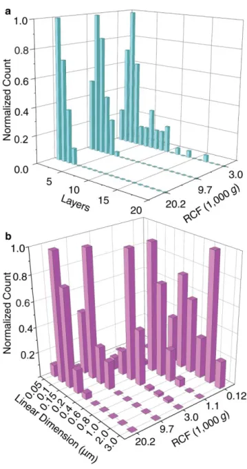
a speed higher than the first run. The sediment was collected and redispersed in fresh solvent. Depending on choice of centrifugation speeds, these fractionated suspensions contained 2DMs with narrow and systematically varying thicknesses distributions (see Fig. 3-4 a,b).
As a typical example, a distribution could be collected at RCF values between 17,200g and 23,400g. The tube would first be spun at 17,200g for 30 minutes. The resulting supernatant would then be removed and re-centrifuged at 23,400g for 30 minutes. The sediment from the second centrifuge would then contain a distribution of flakes that could then be redispersed into any solvent (often we chose IPA) for further analysis; for simplicity, we label this new suspension as 20,200g, the average RCF between the two sequential centrifugation steps. All solution transfers between centrifuge tubes were performed inside a glove box. High speed centrifugations (>12,000g) were performed at 4 °C to lengthen tube lifetime. Following the final centrifugation steps, 2DM suspension are then ready for deposition as films, optical characterization, or preparation as transmission electron microscopy samples.
Table 2-1. Labeling of centrifugation fractions containing 2DM suspensions Sequential RCF (g) Label (1,000g)
30 to 480 0.12
480 to 1,900 1.1
1,900 to 4,300 3.0
7,700 to 12,000 9.7
19
2.3 Advanced transmission electron microscopy techniques for 2D materials
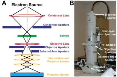
In electron microscopy, an electron wavefront is used to illuminate samples. Compared to optical microscopes, a standard electron microscope appears similar in construction, and consists of an electron emission source, followed by a series of apertures and magnetic lenses to refocus diffracted and transmitted electron beams and ultimately reproduce an image on a phosphor screen (Figure 2-1).
Figure 2-1. Electron Microscope Optics and Design: (A) Theoretical design of microscope column with lens and apertures for the projection of an electron image and (B) a JEOL 100 CX TEM for low-resolution imaging. Taken at CHANL, UNC Chapel Hill.
Despite these similarities, fundamental differences between the physics of electron and light optics enable TEM to achieve high spatial resolution, phase-contrast images, and coherent scattering of electrons. In the proceeding sections, I discuss the important TEM and TEM simulations techniques I developed or applied during my Ph.D. for the study of 2D materials, as well how they relate to the underlying physics of electron optics.
2.3.1 Edge contrast analysis
20
electrons that reach the detector. Differences in intensity due to the presence of a sample causes contrast (Eqn. 2.1) in the resulting image.
𝐶 =𝐼−𝐼0
𝐼 (2.1)
There are three primary types of contrast in TEM: mass-thickness contrast, diffraction contrast, and phase contrast. In mass-thickness contrast, Rutherford scattering of the electron beam from atomic nuclei will lower the intensity and is dependent on atomic number Z, sample density, and thickness.
Previously, it has been shown that mass-thickness contrast can be used to determine the thickness of amorphous, biological, and metallic samples due to the linear relationship between specimen thickness and measured contrast8-14. However, special care must be taken during TEM imaging to limit the other contributions to contrast. For example, diffraction contrast caused by the elastic scattering of electrons from defects, tilted or ‘bent’ samples, or Bragg diffraction from crystal planes, can be removed by appropriately placing the objective aperture in the center of the optical axis so that only the transmitted electron beam is projected. In addition, phase contrast due to the phase shift in diffracted beams is present in every sample, however, its visualization relies on high accelerating voltages (>200 keV) for better resolution, small spherical aberrations for a coherent phase-shift, and higher magnifications to observe the spatial frequency of phase contrast. While these factors are critical for HRTEM image formation, they have little bearing on low resolution techniques where contrast is primarily from mass-thickness.
21
exfoliated 2D materials should also be a stepwise function, and that the smallest possible contrast is that of monolayer flake. The contrast from any flake is then a multiple of the smallest possible contrast and can be used to assign the thickness of any flake observed. I now present a detailed method for conducting an edge contrast analysis of a 2DM suspension of phosphorene, as well as selection bias and potential sources of error.
i. Sample Preparation – In a glove box, 2DM suspensions in IPA or NMP were dropcast (~10 µL) onto a 300-mesh copper TEM grid coated with Lacey carbon (Ted Pella). After deposition, the solvent was evaporated for one hour (IPA) or at least 48 hours (NMP). During this period, TEM grids were held with self-closing tweezers and were not blotted against filter paper to ensure that a representative distribution of the material was deposited. For air sensitive samples, the TEM grids were placed in a grid box wrapped in aluminum foil, placed in a nitrogen-filled zip-loc bag, and brought to the TEM. Grids were rapidly transferred into the TEM with a minimal amount of light exposure. A JEOL 100CX II TEM was used for low resolution imaging. The TEM was operated at 100 kV accelerating voltage and had a resolution of 2 Å (lattice) and 3 Å (point to point).
ii. Alignment – The microscope was carefully aligned, including objective lens, condenser lens, gun position, eucentric height and sample tilt. The latter two alignments are of critical importance to ensure there is no change in defocus or variation in sample height when translating across the grid. When a TEM is improperly aligned, diffracted electrons are not refocused in the image to the point of origin, causing an artificial (diffraction) contrast in the image.
iii.Imaging – A charge-coupled device (CCD) camera was used to acquire all TEM images. The
22
artifacts or variation in background seen in the resulting images. Each image was taken at identical imaging conditions including exposure time, magnification, and defocus value. All images were taken at Scherzer defocus with a complete refocusing of diffracted electrons, and only minor, if any, defocus adjustments were necessary between samples. No pictures were analyzed near the edge of the grid bars, due to the artificial uniform increase in brightness. iv.Contrast Analysis - Contrast changes across phosphorus flake edges were measured by
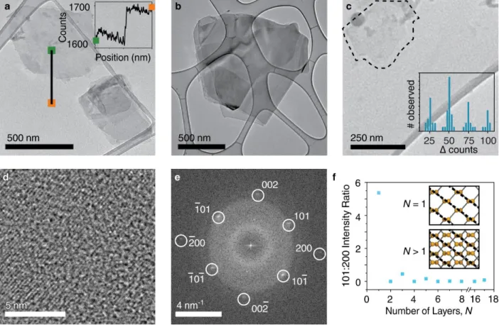
drawing a line profile across and perpendicular to the edge of the flake (Fig. 3.a, line and inset) using Gatan Digital Micrograph.. To first establish the thickness-contrast relationship for our TEM, I measured contrast change for 500 flakes and found that the smallest intensity change was 25 ± 3 counts and all other intensity changes were multiples of 25 counts (Fig. 3.c, inset). I therefore assigned an intensity change of 25, 50, 75, and 100 counts to monolayers, bilayers, trilayers, and four-layered 2D phosphorus flakes, respectively. I note that in some cases, the edge of the flake was over vacuum, and in other cases it was over a carbon film. The maximum difference between the two measurements was 9 counts, and the average difference was 4.4 ± 3.0 counts (N = 12). These numbers are considerably smaller than the average counts per layer of 25 ± 3 counts. I conclude that there was, in general, a negligible difference between these two cases.
v. Sample Selection – The analysis of edge contrast is central for the accurate determination of the optical properties of 2D phosphorus, however it also has the highest potential to introduce an analytical bias. We have identified the five most common occurrences for bias in the contrast analysis and here report their prevalence or prevention.
non-23
uniform contrast to the flake and lacey carbon film. To account for this, we evaporated our solvent for extended periods of time (30 minutes to 48 hours) under vacuum. Samples with a non-uniform contrast due to organics were discarded from our analysis. This error is independent of flake thickness and we find that c.a. 10% of samples across all three suspensions were affected by organic residue. We note that thermal degassing could further eliminate organic residue.
b. Polycrystallinity: Phosphorus flakes with a large degree of polycrystallinity will always exhibit some amount of diffraction contrast that is not uniform across the flake, no matter how well the microscope is aligned or focused. We removed these flakes with a low speed centrifugation (500 RPM), and any flakes imaged showing diffraction contrast were not included in our final analysis. These flakes were c.a. 10% of all three combined phosphorus suspensions.
c. Multilayer flakes: The presence of flakes with more than one distinct thickness is uncontrollable, however this was only somewhat common in the thickest flake distributions (c.a. 15% of flakes have more than one thickness). These flakes are predominantly of one thickness, with >60% of flake area having the corresponding uniform contrast, and were thus assigned to this value for our optical analysis. In the medium and thinner distributions, nearly all flakes exhibited a complete uniform contrast. The overall representation of multilayer flakes for the combined three fractions was c.a. 6%.
24
vapor pressure solvent for TEM samples prepared specifically for edge contrast analysis. Because of the complexity of a 2D phosphorus aggregated structure, flakes can appear to be amorphous, polycrystalline, and have non-uniform contrast. We have chosen to not analyze any flakes that are a component of an aggregate.
e. Lateral Size: An important criterion for the proper execution of the edge contrast thickness measurements is constant magnification, however this can complicate the analysis of small 2D phosphorus flakes (<15 nm linear dimension for our chosen magnification). We have sought to analyze all flakes with size larger than 15 nm, and the observation of flakes smaller than this size was rare, (c.a. <1%). After applying the following techniques to eliminate sample bias, we believe we have accurately accounted for a representative sample of 2D phosphorus flakes in each suspension.
2.3.2 Electron diffraction and Fast-Fourier transforms (FFTs) to determine material thickness
For a given accelerating voltage, an emitted electron beam has a corresponding
wavelength, λ. As electrons pass through a crystalline sample, they are scattered at some angle off of the optic axis with a corresponding phase shift. When this phase shift, or the path length difference, is equal to a multiple of λ (also known as meeting the Bragg condition), there is a constructive interference of diffracted beams. By altering the imaging conditions of the TEM with objective apertures and lens strength, a single diffracted beam can be projected as a dark field image, or each diffracted beam can be focused to create a spot pattern containing
information on crystal structure and lattice spacing.
25
passes through all of the atoms of a unit cell will have a strong intensity in the diffraction pattern. There are 219 distinct space groups for crystals, and since a diffraction pattern is a
two-dimensional projection of a 3D scattering event, both the symmetry and the orientation (zone axis) of a crystal is necessary to extract information on crystal structure and lattice constants.
2DMs present an interesting case for electron diffraction. Large changes in crystal symmetry can occur for monolayer, bilayer, and trilayers of 2DMs. We take advantage of these changes in symmetry to identify monolayer 2DMs using a careful analysis of diffraction patterns and FFT and a comparison to electron simulation. Here I describe the two critical techniques to characterize the thickness of 2DM using diffraction:
1. Obtaining experimental diffraction patterns (DPs) and FFT:
26
Once a suitable sample was found the smallest selected area aperture was inserted and positioned over the flake. The TEM was switched to SA diffraction mode and a diffraction pattern would then illuminate the phosphor screen. To capture the pattern, the camera was inserted and a 0.1 s exposure time and 83 cm camera length were used. Immediately after the image is taken, the camera was removed to prevent damage to the CCD. The image can then be analyzed using Gatan Digital Micrograph to confirm that flakes are crystalline and oriented perpendicular to the electron beam.
Liquid exfoliation can result in flakes that have lateral dimensions too small to reliably observe a diffraction pattern. To characterize the thickness of these samples, a high-resolution JEOL 2010F-FasTEM at 200kV accelerating voltage was used to obtain FFTs. In addition to the previously outlined criteria for sample selection, flakes exhibiting strong phase-contrast are highly crystalline and ideal for FFT analysis. FFTs are easily obtained by capturing the back focal plane during standard HRTEM imaging. The resulting DPs (FFTs) from low resolution (high resolution) TEM can then be compared to electron microscopy simulations.
27
Diffraction patterns were generated in JEMS with a straightforward application of structure factor for diffracting crystals, however, simulations for FFT are sensitive to HRTEM components and imaging conditions. The most important aspect of modeling FFTs is an accurate depiction of the contrast transfer function (Eqn. 2.2, 2.3).
𝑇(𝑘⃑ ) = exp[2𝜋𝑖𝜒(𝑘⃑ )] (2.2)
𝜒(𝑘⃑ ) = 0.25𝐶𝑠𝜆3𝑘4+ 0.5𝛥𝑧𝜆𝑘2 (2.3)
The CTF determines the contrast observed for elements of an image with a given spatial frequency (k), and relies on the accelerating voltage (wavelength) of the electron beam, the spherical aberration Cs, and the defocus value z. Typically, Scherzer defocus (Eqn. 2.4) is chosen as a value of z to minimize the number of nodes in the CTF, thus simplifying the interpretation of the FFT and maximizing the range of frequencies observed in the image.
∆𝑧 = (43𝐶𝑠𝜆)1/2 (2.4)
28
all even layered flakes, severely diminished (<1.0) for odd layered flakes greater with 3 or more layers, and strong (>>1.0) for a monolayer.
2.4Temperature- and pressure-dependent electrical measurements on 2DM films
For metals and semiconductors, conductivity measurements are extremely important for the extrapolation of other electrical properties such as mobility, carrier concentration, and activation energy. Films of 2DMs present an interesting case for electrical measurements: individual flakes have high in-plane electrical transport, but interlayer transport is dominated by tunneling events due to the large van der Waals distance and low orbital overlap. Given the anisotropy of individual 2DM flakes, it is easy to infer a strong structure-property relationship for the electrical properties of reassembled 2DM films, including porosity, contaminants, and turbostratic disorder. To assess this relationship, I measured the conductivity of and activation energy for charge transport in 2DM films using uniaxial pressure and temperature-controlled van der Pauw resistivity measurements.
2.4.1 Van der Pauw geometry for conductivity and activation energy
In 1958, L.J. van der Pauw and coworkers developed an alternative approach to
measuring the conductivity of samples with arbitrary shape15. Four contacts can be made around the perimeter of the sample, labeled A, B, C and D (Figure 2-2). A current is then sourced from contact A to B, and the potential measured from C to D. The resistance, for this orientation of measurement is given by the following equation:
29
Figure 2-2. Common van der Pauw resistivity measurement geometries: (A) Circular sample with four contact points at the perimeter. (B) Cloverleaf geometry for Hall measurements. (C) Amorphous sample geometry
Given the four contacts points, there are four orientations for resistance measurements that can be taken and are as follows: RAB.CD, RBC.DA, RCD.AB, and RDA.BC. The average resistance for a current applied in a vertical orientation (Rv) and a horizontal orientation (Rh) can then be calculated.
𝑅𝑣 = 𝑅𝐴𝐵.𝐶𝐷+𝑅2 𝐶𝐷.𝐴𝐵 (2.6)
𝑅ℎ = 𝑅𝐵𝐶.𝐷𝐴+𝑅𝐷𝐴.𝐵𝐶
2 (2.7)
These resistances can be then be used to solve for sheet resistance, Rs, using the following relationship:
exp (−𝑅𝑣𝜋
𝑅𝑠) + exp (−
𝑅ℎ𝜋
𝑅𝑠 ) = 1 (2.8)
Finally, it is a simple calculation to convert sheet resistance to conductivity:
𝜎 =(𝑅1
𝑠𝑑) (2.9)
where d is the thickness of the sample in either centimeters or meters and σ is conductivity in S/cm or S/m.
30
𝜎 = 𝜎𝑚𝑖𝑛𝑒𝑥𝑝(−𝐸𝑎
𝑘𝑇) (2.10)
where Ea is the activation energy for charge transport, k is Boltzman’s constant and T is
temperature. Plotting ln σ vs. 1/T can then be used to extract Ea as the slope of the line, as seen in Eqn _:
𝑙𝑛(𝜎) =−𝐸𝑎
𝑘𝑇 + 𝐴 (2.11)
I found that 2DM films follow the ln σ ~ 1/T relationship closely (See section 4.4) with minor deviations from linearity. Given that electrons must tunnel across vdW gaps, contaminants, or pores, it is expected that there is a good fit to the hopping model for 2DM films.
2.4.2 Preparation of vacuum filtered films
31
Figure 2-3. 2DM Films with electrical contacts: (A) Vacuum filtered film of MoS2 with four contact points made at the periphery of the film. Nickel wires are adhered to the contact points using silver epoxy. (B) Langmuir-Blodgett trough film of MoS2. Films were deposited onto a Teflon substrate and contacts are made with conductive copper tape. Wires can be adhered to the copper tape with silver epoxy or soldering.
Typically, 5 nm of chrome followed by 50 nm of gold were sputtered onto the film . This ensures that only the film and a small portion of the contact pads will experience the force of the pellet press. Four nickel wires were cut to a length of 5 cm and stripped at each end. A conductive silver epoxy (MG Chemicals #8331S-15G) was applied to one end of each wire and place at the end of the contact pad farthest from the film. The film was then heated to 80° C for one hour to finish the application of the epoxy (Fig. 2-3A). Vacuum films were then stored under inert conditions or their electrical properties were immediately measured.
2.4.3 Preparation of LB trough films, post-deposition
An alternative approach to prepare 2DM films was deposition via LB trough. I will describe briefly the relevant details, but I refer the reader to the dissertation of my colleague, Dr. Tyler Farnsworth from the Scott Warren lab, for an in-depth discussion on the preparation of 2DM films using the LB technique.
32
process is considered one cycle of deposition. After annealing, the film can then be resubmerged for additional cycles and to prepare samples with a desired thickness. An additional challenge for this approach is that a flexible substrate is required to pressurize samples. To address this, we prewrapped glass slides with 0.5 in width PTFE tape (TaegaSeal). After the deposition cycles, the PTFE tape was easily unwound from the slide with the deposited 2DM film intact.
The 2DM films on PTFE were then carefully cut with scissors to be 3.0 mm by 3.0 mm and placed in the center of circular piece of insulating paper. To make electrical contacts to the film, 1.0 mm by 5.0 mm strips of copper foil backed with conductive adhesive were adhered to the corners of the film and extended to the edge of the paper. Finally, four nickel wires were attached to the contacts with silver epoxy or soldering, as described in the previous section (Figure 2-3B).
2.4.4 Electrical measurements on 2DM films with pressure and temperature control Prior to electrical measurements, the 2DM films were placed within a hydraulic press. A pellet die was inverted to provide a pedestal (1.0 cm diameter) for samples to be placed and pressurized, while still being able to make electrical contacts to the extended nickel wires (Figure 2-4). The pressure of the sample could then be easily adjusted and recorded using the pressure gauge. To control the temperature of the sample, each component of the die was wrapped with a
33
silicone heating tape (BriskHeat, 0.5 inches by 12 inches) and controlled with an SDC digital benchtop temperature controller. The digital controller thermocouple was placed between the silicone heating element and the die to correctly control the temperature of the system. Finally, an additional thermocouple was placed in contact with the pedestal, either directly above or below the sample, to accurately probe the temperature of the sample.
A Keithley 2636B Sourcemeter was used to make electrical measurements on 2DM films. The Sourcemeter was setup for four-point measurements with Channel A as the source (Sense Hi and Sense Lo ports) and Channel B acting as a voltmeter (Test Hi and Test Lo ports). Shielded Triax cables with adaptors to alligator leads were used to make connections to the nickel wires in a van der Pauw measurement geometry. The entire system was then double wrapped in aluminum foil to prevent the effects of stray electromagnetic fields during electrical measurements. Finally, a nitrogen line was passed through a desiccant and into the aluminum foil sample chamber to prevent undesired side reactions due to an applied bias.
cross-34
sectional SEM. (vii) Using the collected data and thickness, the conductivity and activation energy for charge transport can be calculated with Eqns. 2.8, 2.9 and 2.11 from section 2.3.1. 2.5Application of DFT for 2D materials
Density functional theory has become a robust and quick computational tool to predict new materials and their optical, electrical, and physical properties. For exact solutions of the Schrödinger equation, there is the many-body problem of electron-electron interactions. To simplify this issue, density functional theory uses the ground state electron density to solve for the total energy of the system. This does not come without its limitations, since the use of electron density causes spurious self-interactions so that an exchange-correlation term must be included in the total energy. An appropriate exchange-correlation functional should always be considered depending on the system to be calculated, such as metals, semiconductors, or highly correlated materials.
It is not within the scope of this dissertation to provide an in depth discussion of the history and background of density functional theory, however I highly recommend reading “Density functional theory of atoms and molecules” by Robert G. Parr and Weitao Yang16, “A Chemist’s Guide to Density Functional Theory” by Wolfram Koch and Max C. Holthausen17, and for a more solid state crystals perspective “Fundamentals of Semiconductor, Physical and Material Properties” by Peter Y. Yu and Manuel Cardona18. For future doctoral students who want to learn DFT independently, I would also suggest studying basic quantum mechanics. In this regard, the MIT Opencourseware lecture series by Prof. Allan Adams on Quantum Physics was a great resource for understanding the theory behind a DFT code, such as modeling
potentials, fourier transforms, plane-wave cut off energies, etc. Finally, one of the most
35
now describe the most relevant computational techniques and approaches that I used to study 2D materials and their heterostructures.
2.5.1 General methods using CASTEP
Density functional calculations were performed using the CASTEP19 code with plane-wave basis set20 approximations. Ultrasoft21 pseudopotentials were used to describe core electrons, and a 600 eV cut-off energy was typically used. A GGA PBE functional22 was used for the exchange-correlation contribution to total energy and Grimme’s DFT-D23 correction was used to account for long-range dispersion forces (see section 2.5.2 for additional details). A Monkhorst-Pack24 grid corresponding to an inverse spacing of 0.02 1/Å between k-points was used. In order to calculate a 2DM of varying thickness, a periodic 12 Å vacuum slab was included in the unit cell to prevent self-interactions.
Prior to performing any geometry optimization or property calculations, it is extremely important to check for energy convergence. Internal energy minimization is done with an SCF loop with convergence set to 5.0 x 10⁻⁷ eV/atom and a window of three, however, external testing for convergence should always be performed. There are two important tests: (i) the plane-wave cut off energy should be increased in multiples of 25 eV while recording the total energy, Etot. When the dEtot/dlnEcut is less than 0.01 eV/atom the calculation can be considered well converged. (ii) In a similar manner, the k-point mesh should be increased while monitoring Etot until dEtot/dk-point is less than 0.01 eV/atom.
36
determined values. For layered materials, it also important to include a semiempirical parameter to account for van der Waals forces. A discussion of Grimme’s DFT-D correction is presented in section 2.5.2.
Once a structure was geometry optimized, a subsequent properties calculation could be performed to obtain the band structure, electron density, density of states, partial density of states, and optical properties. For these property calculations, an increased k-point mesh is required for greater accuracy, and therefore I used a 0.0025 1/Å k-point spacing. Furthermore, the number of conduction bands (referred to as extra bands in the Materials Studio and CASTEP interface) will also effect the accuracy of the result. Generally, I specified the number of conduction bands as 10n, where n is the number of atoms in the periodic cell. The exception for this relationship is optics calculations, which required at least 100n conduction bands.
2.5.2 Grimme’s DFT-D correction for dispersion forces
It is well known that the LDA and GGA functionals of DFT will often inaccurately describe the long range intramolecular forces found in van der Waals (vdW) materials. To account for this, I used a semiempirical DFT-D with Grimme’s dispersion correction to solve for the relaxed geometry and minimum energy of our bulk homogenous and heterogeneous layered systems19, 23, 26. The total energy now takes the form of:
𝐸𝑡𝑜𝑡 = 𝐸𝐷𝐹𝑇+ 𝑠𝑖∑𝑁𝑖=1∑𝑗>1𝑁 𝑓(𝑆𝑅𝑅𝑖𝑗0, 𝑅𝑖𝑗)𝐶6,𝑖𝑗𝑅𝑖𝑗−6 (2.12)
37
scaling factors si and SR are dependent on the dispersion scheme chosen: For Grimme’s dispersion correction, si is equal to 0.75 and SR is unity.
The geometry optimization of layered materials with van der Waals forces is drastically improved when Grimme’s DFT-D correction is included. In general, the provided atomic vdW constants from CASTEP are sufficient to optimize structures with lattice constants typically within 2.0% of experimentally determined values, with greatest improvement in accuracy for interlayer distances. One exception is the optimization of graphite, in which I adjusted our vdW constant to 16.34 eV Å6 tobetter describe the interaction of sp2 hybridized carbon in graphite27-28, resulting in an increase in interlayer distance, d, from 3.25 Å to 3.32 Å. This is in much closer agreement with experimentally determined values of 3.36 Å29-30 and this vdW constant was used for all calculations involving multilayer or single layer graphite.
2.5.3 Binding energy, gravitational deformation and phonon modes for 2DM stability From a thermodynamic perspective, 2DMs are a metastable phase of their parent layered material. In this regard, it can be difficult to predict whether a layered material can be exfoliated to the two-dimensional level. I here describe three critical analyses for the stability of a 2DM, including (i) binding energy calculations for interlayer interactions, (ii) the gravitational
deformation of a 2DM as a freestanding material, and (iii) the application of phonon calculations as measure of stress on the 2DM.
(i) Binding energy:
The weak van der Waals forces in graphite result in an interlayer binding energy, EBE, of 35 meV/atom31. Because EBE is approximately equal to exfoliation energy, Eex, its magnitude is often used as a metric to whether a layered material can be exfoliated. Advanced
38
energy for vdW layered materials to be 10-20 meV/Å2. While there can be errors in the EBE when calculated with a GGA PBE functional and Grimme’s DFT-D corrections, it is qualitatively correct in determining structures and predicting trends. Therefore, I used binding energy calculations to determine the binding energy of new layered materials (black phosphorus, layered electrides) and in 2DM heterostructures (Chapter 5).
To calculate EBE, we varied the interlayer distance between individual layers and then calculated the total energy. An ‘infinite’ structure was built with an interlayer distance of 12 Å, such that there were no interactions between sheets. We then calculated EBE as:
𝐸𝐵𝐸 = (𝐸𝑛𝑖𝑙𝑑−𝐸∞)
𝑖𝑛𝑡𝑒𝑟 (2.13)
where E∞ is the energy of the infinite structure, Eild is the energy of the optimized structure, and ninter is the number of atoms at the interface of two layers. Alternatively, EBE can be calculated per unit area, and typically is reported as either meV/Å2 or meV/atom. (ii)Gravitational deformation of 2DM:
An important criterion for the stability of a 2DM is the ability to withstand its own weight. The processing of 2DM for electronic applications and optical measurement requires numerous lift-off and transfer steps, as well as the suspension of these materials as a
membrane. The 2D Young’s modulus of a 2DM can be calculated from an applied strain:
𝑌𝑀2𝐷 =𝑑
2𝐸 𝑠
𝑑𝜖2 ∗ 𝐴−1 (2.14) where Es is the difference in energy between the optimized structure and the strained unit cell, Ɛ is the strain in a single lattice direction, and A is the area of the unit cell. Using the YM2D, the deformation of a 2DM as a membrane can be calculated with Eqn 2.15.
ℎ 𝑙 = (
𝜌𝑔𝑙 𝑌𝑀2𝐷)
39
where l is a lateral dimension of the suspended region, ρ is the density of the material, g is the gravitational force, and h is the deformation of the material in the z direction. It is expected that for a given l, the ratio h/l should be at least <0.001, implying the material can withstand its gravitational weight.
(iii) Phonon dispersions
A final technique to predict the stability of a 2DM is to calculate the phonon dispersions. Phonons are quantized vibrational modes of the atomic nuclei and can be either acoustic or optical. Since phonons are a physical process, they always have positive energies associated with their vibrational wavelength. The observation of negative phonons implies a material is unstable, and that a more stable phase can be found corresponding to the atomic
displacements of the negative phonon.
I calculated the phonon dispersion of layered materials and 2DM using the finite displacement phonon property calculations with CASTEP. First, structures were geometry optimized to a higher degree of convergence than described in section 2.4.1. Particularly, energy, max stress, and max GPa tolerance were increased to 1 x 10⁻¹⁰ eV/atom, 0.001 eV/Å, and 0.001 GPa, respectively. A cutoff radius was chosen so that the supercell was at least four times the volume of the unit cell, in order to accurately model longer wavelength phonon modes. Phonon dispersion spectra were plotted along a Brillouin zone path