FABRICATION AND CHARACTERIZATION OF ALIGNED TITANIA NANOWIRE FILMS FOR SOLAR CELL APPLICATIONS
Zheng Ren
A dissertation submitted to the faculty of the University of North Carolina at Chapel Hill in partial fulfillment of the requirements for the degree of in the Curriculum in Applied Sciences and Engineering.
Chapel Hill 2012
ii ©2012 Zheng Ren
iii
ABSTRACT
ZHENG REN: Fabrication and Characterization of Aligned Titania Nanowire Films for Solar Cell Applications
(Under the direction of Lu-Chang Qin)
A new hydrothermal method has been developed to grow foldable free-standing TiO2 films which are composed of highly aligned rutile nanowires. The rutile phase TiO2 nanowires are grown in the [001] direction. The free-standing film possesses a very high percentage of (110) surface, which is thermodynamically the most stable and well-studied TiO2 surface. Different growth parameters have been investigated and a new growth mechanism of the free-standing film is proposed. The free-standing film shows its stability in many extreme environments. For example, it can maintain the same morphology after high temperature annealing, hydrogen treatment and surface coating. In addition, the free-standing nanowire film can be directly attached to different substrates, some of which have not been reported to support the growth of vertical TiO2 nanowire structures, hence providing another method of fabricating nanowire structures on various substrates. The new process can also avoid damage to the conducting metal oxide layer during the growth process and other treatments.
iv
nanoparticle film. Because the surface area of the semiconductor porous film is essential for the performance of DSSCs, morphology control is fundamentally important for nanowire material growth techniques. By stacking nanowire films layer by layer, a multi-layer assembly photoanode has been built. The multi-multi-layer TiO2 assembly can precisely control the thickness and the surface area of semiconductor photoanode in a DSSC. DSSCs using these multiple-layer electrodes were built and tested. By enhancing the contact between nanowires and the substrate and improving the electrical properties with high temperature annealing, 3.8% efficiency was achieved for a single layer electrode. After attaching three layers together, 4.8% solar energy conversion efficiency was shown for a three-layer of TiO2 film photoanode, demonstrating an efficiency boost of 25% compared with the single layer electrode. The multi-layer assembly photoanode shows a new way to increase and control the roughness of a TiO2 nanowire array, which also helps to improve the performance of a TiO2 electrode in many applications such as solar cell and water splitting.
A new direct-deposit method was developed to build a flexible photoanode utilizing the free-standing foldable TiO2 nanowire film. The new approach provides good electrical interconnection in the TiO2 electrode and obviates the need for high temperature treatment, allowing the device to be constructed on a plastic substrate. A flexible photoanode was built. A DSSC with this design shows a high short circuit current density (8 mA/cm2) and open circuit voltage (0.75 V). An efficiency of 1.5% DSSC was achieved using this photoanode.
v
vi
ACKNOWLEDGEMENTS
Although only my name is on this dissertation, many people have contributed to this production. I owe my great gratitude to all the people who have made this dissertation possible.
It is hard to overstate my gratitude to my supervisor, Professor Lu-Chang Qin. I am very fortunate to have him as my advisor who gave me the freedom to explore on my own. His patience and support helped me overcome many crisis situations and finish this dissertation. For me, he is not only a professor, but also a lifetime friend and advisor.
My special thanks go to the other members of my thesis committee, Dr. Wenbin Lin, Dr. Laurie McNeil, Dr. Rene Lopez, Dr. Alfred Kleinhammes and Dr. Yue Wu for their guidance and helpful discussions. I would also like to express my gratitude to Dr. J.P. Lu, who was willing to participate in my final examination at the last moment.
vii
preparing the flexible photoanode. I want to thank the members in the EFRC device group, Dr. Paul Hoertz, Dr. Leila Alibabaei, Myoung-ryul Ok, Dr. Kyle Brennaman, Hanlin Luo. They have contributed a lot to my dissertation. They gave me the training of the facilities and provided many useful suggestions to improve the efficiency of the solar cells.
I would also like to thank the CHANL members, Dr. Carrie Donley, Wallace Ambrose, Robert Geil and Dr. Amar S. Kumbhar. Without their help, this project is impossible to be finished on time. I appreciate my conversations with Dr. Amar S. Kumbhar. He shared a lot of his experience and knowledge in research, which help me to explore the new applications of the TiO2 nanowires.
I would like to thank EFRC for providing me the financial support and the facility support.
I would also like to thank my parents. They have always been supporting me and encouraging me with their best wishes.
viii
TABLE OF CONTENTS
LIST OF TABLES………...x
LIST OF FIGURES ………...…xi
Chapter I. INTRODUCTION ... 1
II. SYNTHESIS, STRUCTURE AND PROPERTIES OF NANOSTRUCTURED TITANIUM DIOXIDE ... 5
2.1. Properties of Titanium dioxide ... 5
2.1.1. Structure of TiO2 ... 5
2.1.2. Thermodynamic properties of TiO2 ... 8
2.1.3. Electrical and optical properties of TiO2 ... 10
2.1.4. Photocatalytic properties of TiO2 ... 13
2.1.5. Properties of doped TiO2 ... 16
2.2. Synthesis of low dimensional Titanium oxide nanomaterial ... 18
2.2.1. Vapor-liquid-solid method ... 19
2.2.2. Chemical vapor deposition method ... 23
2.2.3. Hydrothermal method ... 24
2.2.4. Electrochemical anodization ... 29
2.2.5. Other synthesis techniques ... 31
2.3. Dye-sensitized solar cells ... 32
ix
2.3.2. Characterization techniques for solar cell ... 44
2.3.3. Flexible dye-sensitized solar cell ... 52
2.3.4. Nanowire based dye-sensitized solar cells ... 53
2.4. Summary ... 54
III. SYNTHESIS AND CHARACTERIZATION OF FLEXIBLE FREE-STANDING TiO2 NANOROD FILM ... 57
3.1. Synthesis of free-standing TiO2 nanowires film ... 57
3.2. Characterizations of TiO2 nanowires on FTO and free-standing film ... 59
3.3.1. Morphology of TiO2 nanowires ... 59
3.3.2. X-Ray diffraction analysis of TiO2 nanowires grown on FTO ... 62
3.3.3. TEM characterization of individual nanowire ... 65
3.3.4. Optical properties of free-standing TiO2 nanowires film ... 67
3.3. Growth mechanism of TiO2 free-standing film ... 69
IV. NANOWIRES FILM BASED DYE-SENSITIZED SOLAR CELLS ... 74
4.1. Motivations ... 75
4.2. Fabrication of TiO2 nanowire electrode on FTO ... 77
4.3. Fabrication of dye-sensitized solar cells ... 82
4.4. Effect of electrode annealed at different temperature on the performance of DSSC... 86
4.5. Effect of stacking multiple layer of TiO2 nanowire films on the performance of DSSC... 97
4.6. Summary ... 109
V. DYE-SENSITIZED SOLAR CELL ON FLEXIBLE SUBSTRATE ... 111
5. 1 Fabrication of flexible dye-sensitized electrode ... 112
5. 2 Fabrication of DSSC using flexible TiO2 electrode ... 120
x
xi
LIST OF TABLES
Tables
Table 3-1. Sheet resistance of FTO after different time length growth ... 73 Table 4-1. Efficiency of DSSCs using electrodes at different
annealing temperatures. ... 88 Table 4-2. Fitted parameters for DSSCs using the electrode annealed
at different temperatures. ... 92 Table 4-3. Estimated parameters for electrodes annealed at different
temperatures. ... 94 Table 4-4. Efficiency of DSSC using free-standing film. ... 103 Table 4-5. Fitted parameters for EIS measurements of multiple layer
electrodes. ... 106 Table 5-1. Effects of post treatments on the sheet resistance of ITO
xii
LIST OF FIGURES
Figure
Figure 1-1. Roadmap for the development of solar cell efficiency.13 The world record efficiency of a solar cell is 43.5%, which was achieved by a three-junction solar cell. However, the unaffordable cost of multijunction solar cells limits their application. Silicon solar cells have obtained 20% efficiency for multicrystalline silicon and 27% efficiency for single crystal cells, which make it the most widely used solar cell. Dye-sensitized solar cell is one of the most efficient third generation solar cells. It recently achieved
12% efficiency and shows a promising future. ...3 Figure 1-2. Schematic diagram of a dye-sensitized solar cell. ... 5 Figure 2-1. Bulk structure of rutile and anatase. The stacking of the
octahedra in both structures is shown on the right side.49 ...7 Figure 2-2. Enthalpy of nanocrystalline TiO2 in different phases.58 ... 10 Figure 2-3. Conductivity of anatase and rutile thin film.63 Sample 1 is
the TiO2 film deposited using sputtering; Sample 2 is a TiO2 film which has been reduced in H2 at 400 ℃; Sample
2 is a TiO2 film which has been reduce in H2 at 450 ℃. ...12 Figure 2-4. Conductivity of anodized TiO2 nanotube after annealing at
different temperatures.64 ...13 Figure 2-5. Band gap positions of several metal oxides.66 ... 15 Figure 2-6. The absorption of TiO2 and N-doped TiO2.76 Compared
with pure TiO2, N-doped TiO2 can absorb light of longer
wavelengths. ...17 Figure 2-7. In situ TEM images showed the Ge nanowire growth with
xiii
Figure 2-10. SEM images of MOCVD grown TiO2 nanorods in Wu’s study.111 A is rutile TiO2 nanorods and B is anantase TiO2
nanorods. ...24
Figure 2-11. Cross-section of hydrothermal method grown TiO2 nanowire array on Ti substrate.119 ...26
Figure 2-12. TiO2 nanowire grown in toluene on TCO substrate.61 ... 27
Figure 2-13. TiO2 nanowire array growth using water as the solvent.120 ... 28
Figure 2-14. SEM image of anatase TiO2 with large percentage of (001) surface.60 . 29 Figure 2-15. SEM images of 33 𝜇𝑚 titania nanotubes grown on FTO glass.128 ... 30
Figure 2-16. SEM images of anodic aluminum oxide template. a) Top view and b) Cross section.135 ...32
Figure 2-17. Schematic diagram of dye-sensitized solar cells. ... 34
Figure 2-18. Transmission spectrum of pulsed direct current magnetron sputtering prepared FTO.158 ...36
Figure 2-19. IPCE of DSSC using black dye.166 ... 38
Figure 2-20. Photocurrent vs voltage plot of DSSC using black dye.166 ... 39
Figure 2-21. Overview of the time constants for the processes in a working dye-sensitized solar cell.69 ...41
Figure 2-22. The electron configuration in the DSSC.15 ... 43
Figure 2-23. I-V curve of a typical dye-sensitized solar cell. ... 45
Figure 2-24. The modified equivalent circuit for a working solar cell. ... 46
Figure 2-25. Illuminated I-V sweep curve. ... 47
Figure 2-26. Estimating series resistance and shunt resistance from I-V curve. ... 49
xiv
Figure 2-28. Equivalent circuit of dye-sensitized solar cell.178 ... 52 Figure 2-29. Schematic diagram of using nanowires as photoanode in
dye-sensitized solar cells.26 ...53 Figure 2-30. Schematic demonstrates the advantage of using
nanowires as photoanode for a flexible dye-sensitized solar
cell.145 ...54 Figure 3-1. Schematic diagram of the hydrothermal synthesis of TiO2
nanowire film. ...58 Figure 3-2. a) The 1 cm by 2 cm free-standing film is folded and
placed on a page of yellow paper with nanowires facing outside. b) The free-standing film is placed on a blue UNC
logo print. It shows the semitransparency of the white film. ...59 Figure 3-3. TiO2 nanowires grown at 150 ℃ for 4 hours: a) cross
section of TiO2 nanowires grown on FTO, b) top view of
nanowires. ...60 Figure 3-4, SEM results of TiO2 layer using 3 ml titanium butoxide. ... 61 Figure 3-5. a) Cross sectional SEM image of the film, scale bar is 2.5
𝜇𝑚; b) Top view of the free-standing film, which is made of highly ordered nanowires, scale bar is 2 𝜇𝑚; c) bottom layer of the film, scale bar is 1 𝜇𝑚; d) folded film, scale bar
is 50 𝜇𝑚. ...62 Figure 3-6. XRD spectrum of as grown TiO2 nanowires on FTO. ... 63 Figure 3-7. XRD spectrum from free-standing TiO2 film (Top) and the
power sample prepared from film. ...64 Figure 3-8. EDS spectrum from the back side of free-standing film. ... 65 Figure 3-9. HRTEM images and nanobeam diffraction pattern of an
individual TiO2 nanowire. ...67 Figure 3-10. Absorption spectrum of rutile TiO2 film from both sides. ... 68 Figure 3-11. Comparisons of transmission, reflection and absorption
xv
Figure 3-12. Cross section of TiO2 nanowires grown on FTO with
different growth times. ...70 Figure 3-13. Relationship between film thickness and growth time. ... 71 Figure 3-14. Topview SEM images of TiO2 nanowire grown on FTO
with different growth time. ...72 Figure 3-15. Schematic diagram of free-standing film growth
mechanism: first, TiO2 nanowires start to grow from nuclei on FTO in the autoclave; and short aligned nanowires are then obtained; these nanorods keep growing and some new nanorods start to emerge among the longer nanowires and form a dense short TiO2 rods layer under the longer nanowires; a compact TiO2 layer forms under the nanowires; once the titanium precursor runs out, nanowires stop growing. In a high temperature environment, the acid etches the FTO layer through the porous TiO2 nanorods
layer. A white film can be peeled off from the substrate. ...73 Figure 4-1 Fabrication scheme of nanowire photoanode from a
free-standing TiO2 film...77 Figure 4-2. Schematic diagram of two types of nanorod based solar
cell. The arrangement on the left is called the face up
design and at right is the face down design. ...78 Figure 4-3. Single layer elcetrode fabricated with different
spin-coating speed. a) 3000 r.p.m. face up design; b) 3000 r.p.m. face down design; c) 5000 r.p.m. face up design; d) 5000
r.p.m. face down design. Scale bar is 1 𝜇m. ...79 Figure 4-4. SEM images of multiple layer TiO2 nanowire electrode
with different designs. a) Single layer face up design, b) double-layer face up design, c) triple-layer face up design,
d) one layer with face down design. Scale bar is 1 𝜇𝑚. ...81 Figure 4-5. Schemetic diagram of solar cell fabrication procedure: a)
xvi
hole was sealed with a piece of polymer and the electrolyte
was injected, h) the cell was sealed. ...83 Figure 4-6. Structure of nanowire based DSSC. The solar cell will be
illuminated from the back side of the TiO2 electrodes. The
distance between the two electrodes is 25 𝜇𝑚. ...85 Figure 4-7. J–V measurement of electrodes annealed at different temperatures. ... 87 Figure 4-8. Equivalent circuit for the electrodes in dye-sensitized solar
cells. A) represents the resistance of the TCO glass, B) represents the Pt-electrolyte interface and C) represents the
TiO2-electrolyte interface. ...89 Figure 4-9. Spectra of EIS for cells made of electrodes annealed at
different temperatures. ...90 Figure 4-10. effective electron diffusion coefficients of electrodes
annealed at different temperatures. ...95 Figure 4-11. Roughness factor (RF) vs the number of layers for TiO2
nanowire arrays with two photoanode structures. ...99 Figure 4-12. IPCE of solar cells with multi-layer face-up electrode
design. IPCE results showed that the photon to current efficiency was increased when more layers were stacked onto the electrode, which agrees with the measurement of
the short circuit currents...100 Figure 4-13. Absorption spectrum of single and double layer of
sensitized TiO2 nanowires film on FTO glass. ...101 Figure 4-14. Photovoltaic performance of DSSC fabricated using TiO2
nanowire arrays in different electrode structures: (a) I-V characteristics of solar cell with multiple layer face-up electrode design; (b) I-V characteristics of solar cell with
single layer face-down electrode design. ...103 Figure 4-15. Fitted EIS results for multiple assemblies with face up design. ... 104 Figure 4-16. Estimated the electron density in the conduction band and
the total number of electrons in the conduction band for the
cells. ...108 Figure 5-1. Schematic diagram of fabricating on of a nanowire based
xvii
free-standing TiO2 nanowire film to a conducting substrate directly using a conductive adhesive layer, a flexible photoanode can be fabricated. a) the TiO2 free-standing film was annealed at 450 ℃ to enhance the internal connection of the nanoparticle layer, b) An adhesive layer was spin-coated onto a commercial conductive flexible substrate, c) The prepared TiO2 film was attached to the
adhesive layer...113 Figure 5-2. Schematic diagram of fabricating a flexible photoanode
using the “direct deposition” method: a) a) free-standing hybrid TiO2 film was prepared using the doctor blading method on the TiO2 nanowire film; b) the free-standing TiO2 hybrid film was annealed at 450 ℃ to enhance the internal electrical properties; c) a 200nm thick ITO layer was deposited onto the back side of the free-standing film using PLD; d) a supportive substrate was attached to the
prepared sample. A flexible photoanode is obtained. ...115 Figure 5-3. Cross section of hybrid TiO2 electrode. 7 𝜇m thick
nanoparticle film was coated at the top of a flexible TiO2 nanowire film. 200 nm ITO layer was deposited from the
back side of the hybrid flexible electrode. ...116 Figure 5-4. PLD deposited ITO layer on TiO2 film. A 200nm thick
ITO layer was deposited at the bottom of the film. ...117 Figure 5-5. Demonstration of a flexible photoanode. ... 119 Figure 5-6. Schematic illustration of flexible TiO2 film based electrode.
Part of the flexible photoanode film was attached to a supporting substrate using PMMA. The other free-standing part was used to provide the electrical connection to the
outer circuit. ...120 Figure 5-7. Schematic illustration of sample holder for solar cells
fabricated by the “direct deposition” method. The sample holder was used to prevent the deformation during the measurements. The two electrodes of the solar cell were connected with gold connectors. During the measurements,
the flexible photoanode was kept flat. ...122 Figure 5-8. IPCE of the solar cell fabricated by the “direct deposition”
xviii
electrode helps to increase the dye loading and the IPCE of
the photoanode. ...123 Figure 5-9. J-V curve of the solar cell produced using the “direct deposition” method. ... 124 Figure 5-10. Full J-V curve of solar cell using flexible hybrid nanowire
electrode in light and in dark. ...125 Figure 5-11. EIS result for low temperature fabricated DSSC using
xix
ABBREVIATIONS
CVD Chemical vapor deposition DSSC Dye-sensitized solar cell
EIS Electrochemical Impedance Spectroscopy FTO Fluorine doped Tin Oxide
ITO Indium tin oxide
CHAPTER 1
INTRODUCTION
Energy consumption worldwide heavily depends on fossil fuels, such as oil and coal. However, the world has recognized that the supply of fossil fuel is limited while the demand for fuel is still on the rise. There is a pressing challenge to develop new types of clean energy to provide for energy consumption in the future, for the following reasons: limited supply of fossil fuel, global climate change as a result of fossil fuel consumption, and environmental issues. The next generation of clean energy needs to be safe, environmental friendly and low-cost. Among those, nuclear energy, wind energy and solar energy have attracted enormous research interests and have shown the most potential in solving the current energy crisis.
2
3 F igu re 1 -1 . R oa dm ap f or t he de ve lopm ent of s ol ar c el l e ff ic ie nc y . 1 T h e w o rl d r eco rd ef fi ci en c y o f a so lar cel l is 43.5% , w hi ch w as a ch ie ve d b y a th ree -j un ct ion s ol ar c el l. H ow eve r, t he una ff or d abl e c os t of m ul ti junc ti on so la r c ells limits th eir a p p lic atio n . S il ic o n s o la r c ell s ha ve obt ai n ed 2 0 % e ff ic ie n c y f o r mu ltic ry st allin e s ilic o n an d 2 7 % ef fi ci en c y f o r s in g le cr y st al cel ls , w h ic h ma k
e it th
4
Figure 1-1 summarizes the current efficiency progress of different types of solar cells.1 Silicon solar cells have shown the ability to achieve a high efficiency, 20% efficiency for multicrystalline silicon and 27% efficiency for single crystal silicon. The high efficiency and mature production technology have made the silicon solar cell the most widely used solar cell so far. However, the high cost and the environmental issues during the fabrication of silicon based solar cells forced researchers and scientists to look further for other low-cost solutions to achieve similar solar energy conversion efficiency.
5
Figure 1-2. Schematic diagram of a dye-sensitized solar cell.
Nanowires and nanotubes have exhibited unique morphological, electrical and optical properties and have been employed in many applications, such as energy conversion,16-18 chemical sensors,19-22 and field effect transistors.23-25 TiO2 nanowires have shown the capability to be an excellent photoanode material for dye sensitized solar cells. Compared with the TiO2 nanoparticle film widely used in DSSCs, single crystal TiO2 nanowires have fewer trapping sites which can cause electron recombination and photo-current loss in solar cells. Vertically grown nanowires can also provide the shortest electron transfer pathway from the top of nanowires to the substrate.26, 27
6
Moreover, because substrates have different surface energies and surface structures, many efforts are required to control the morphology of nano materials on different substrates.29, 30
CHAPTER 2
SYNTHESIS, STRUCTURE AND PROPERTIES OF NANOSTRUCTURED TITANIUM DIOXIDE
2.1. Properties of Titanium dioxide
As the most promising photo catalyst, TiO2 is expected to play a key role in helping to degrading organic pollutants.31 Because of the discovery of its photo water splitting property and the invention of high efficiency dye-sensitized solar cells, TiO2 has attracted much attention and many development efforts.11, 32, 33 The properties of TiO2 were intensively investigated in the last century.34-37 Along with the development of nanotechnology and nanoscience, some unique properties of TiO2 were discovered when its grain size was reduced to several nanometers and new applications were developed using TiO2 nanomaterial.38-40
2.1.1. Structure of TiO2
6
7
Figure 2-1. Bulk structure of rutile and anatase. The stacking of the octahedra in both structures is shown on the right side.49
8
lattice constants for anatase are a=3.784 Å and c=9.515 Å, which result in different mass densities between rutile and anatase (4.25 g/cm3 vs 3.89 g/cm3).
2.1.2. Thermodynamic properties of TiO2
Rutile is the thermodynamically stable phase of TiO2 at all temperatures and the rutile (110) surface is thermodynamically the most stable surface of the structure.48, 50-52 After high temperature annealing, other surfaces will be reconstructed to rutile (110) surface to achieve the lowest energy. The transformations of nanocrystals among the three phases of TiO2 have been intensively studied. Czandern et al. systematically studied the anatase to rutile transformation under different annealing conditions.43 They suggested that no transformation occurred below 610℃ and the conversion became rapid once temperature was above 730 ℃ for anatase power. Zhang observed that anatase and brookite nanocrystals were transformed to rutile during the synthesis process when the nanocrystals reached a certain particle size.53 Li also reached a similar conclusion that small anatase nanoparticles were observed to aggregate to form larger rutile nanoparticles when they reached a certain size during synthesis and larger rutile particles interact with surrounding anatase nanoparticles to form larger size rutile particles.54 Ye and co-workers reported that there was slow transformation from brookite to anatase below 1053 K and both brookite–to–anatase transformation and anatase–to–rutile transformation were observed to occur very fast between 1053 K and 1123 K. When the temperature reaches above 1123 K, only rutile grain growth is observed and rutile becomes the dominant phase.55
9
∆G =∆H−T∆S 2-1
10
Figure 2-2. Enthalpy of nanocrystalline TiO2 in different phases. 58
According to the results described above, TiO2 nanocrystals need to have at least one dimension less than 35 nm to maintain their anatase structure.59 However, abnormal behavior and inconsistent results have been occasionally observed. Anatase particles of over 1 micron have been synthesized when aqueous HF acid is present in the reaction.60 This is because fluorine ions were absorbed by the surface of the TiO2 particles and the energy of the anatase surfaces was changed, suppressing the formation of rutile structures. Feng et al. reported that rutile nanowires 20 nm diameter were synthesized in toluene in a hydrothermal reaction.61
2.1.3. Electrical and optical properties of TiO2
11
crystalline rutile was measured and reported by Cronemyer in the temperature range of 300℃ to 1400℃.62 According to his results, the relationship between conductivities of rutile at different temperatures in different crystallographic directions can be calculated using the following equations, where 𝜎 is the electrical conductivity in (ohm cm)-1 and T is the absolute temperature.
Directions perpendicular to c axis
ln𝜎= 7.92−11600/𝑇, 623 K to 1123 K 2-2
ln𝜎= 11.10−21200/𝑇, 1123 K to 1673 K 2-3
Directions parallel to c axis
ln𝜎= 8.43−17600/𝑇, 773 K to 1223 K 2-4
ln𝜎= 11.30−21200/𝑇, 1223 K to 1673 K 2-5
12
compared with as-grown films. The conductivity of rutile films showed a steady decrease as the annealing temperature increased and the conductivity of rutile also decreased when measured at higher temperatures. These results suggest that undoped rutile could have a higher conductivity than undoped anatase after high temperature annealing.
Figure 2-3. Conductivity of anatase and rutile thin film.63 Sample 1 is the TiO2 film deposited using sputtering; Sample 2 is a TiO2 film which has been reduced in H2 at 400 ℃; Sample 2 is a TiO2 film which has been reduce in H2 at 450 ℃.
13
Figure 2-4. Conductivity of anodized TiO2 nanotube after annealing at different temperatures.64
2.1.4. Photocatalytic properties of TiO2
14
TiO2 electrode and the platinum electrode without external bias voltage. The steps of the reactions are described as following:
TiO2 +2ℎ𝜈
�⎯⎯�2𝑒−+ 2p+ (excitation of TiO
2 by light) 2-6 2H2O + 4p+ �⎯⎯�O2+ 4H+ (at the TiO2 electrode) 2-7
2H++ 2𝑒+ �⎯⎯�H
2 (at the platinum electrode) 2-8
The overall reaction is
2H2O +4ℎ𝜈
�⎯⎯�O2 + 2H2 2-9
15 Figure 2-5. Band gap positions of several metal oxides.66
TiO2 has a 3.0 eV band gap, meaning that it can absorb only UV light to decompose water. Sunlight contains only a small amount of UV light. Even if the efficiency of the decomposition reaction is very high, only 3% efficiency can possibly be achieved in the solar spectrum.69 The electrolysis of water requires 1.23 eV to split the water molecule, which suggests that a semiconductor with a band gap close to 1.3 eV is more desirable for photo water splitting and photocatalytic applications.
70-16 72
TiO2 has also shown the ability to kill tumor cells.72, 73 In these studies, TiO2 decomposed organic compounds by an oxidization reaction under sunlight. In the photo-induced oxidation reaction, the conduction band position of the semiconductor determines its oxidation capability. Because anatase has a more negative conduction band and a lower recombination rate, anatase has been observed to be a more active photocatalyst than rutile when O2 is the oxidizing agent.74, 75
2.1.5. Properties of doped TiO2
Because TiO2 only absorbs light of wavelength less than 415 nm, it limits the overall photocatalytic efficiency. Modification of the band gap structure of TiO2 is expected to improve the photocatalytic and electrical properties of TiO2 nanocrystals. Many attempts have been made to decrease the band gap of TiO2. However, because the conduction band position is an important factor for its catalytic properties, these modifications must meet the following criteria: 1) have the same conduction band position as TiO2 or a more negative one; 2) reduce band gap or create a state in the middle of the band gap to absorb the visible light and 3) the newly created states need to overlap sufficiently with the states of TiO2 to transfer photoexcited carriers to its catalyst surface within their lifetime. Different elements have been doped into TiO2 and some improvements for photocatalytic applications have been observed, such N-doped TiO2, C-doped TiO2 and hydrogenated TiO2.
17
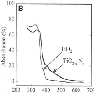
that doping by N was the most effective because its p states can contribute to narrowing the band-gap by mixing with O 2p states in TiO2. The calculated results agreed with their experimental results. N-doped TiO2 was prepared using sputtering in N2 gas. The absorption of N-doped TiO2 was extended to 550 nm as shown in Figure 2-6 and N-doped TiO2 showed the enhanced photocatalytic ability.
Figure 2-6. The absorption of TiO2 and N-doped TiO2.76 Compared with pure TiO2, N-doped TiO2 can absorb light of longer wavelengths.
Carbon was also found to be an effective dopant to reduce the band gap of TiO2. C-doped TiO2 could be obtained by burning Ti foil in a natural gas flame. The band gap of C-doped TiO2 prepared by the flame method was narrowed to 2.32 eV and the maximum photo conversion efficiency was improved to 8.35%. C-doped TiO2 can also be fabricated by heating titanium carbide,77 or annealing TiO2 in CO gas.78
18
and valence band were broadened by the hydrogen treatment, because it induces a disordering in the layer on the surface of TiO2 nanocrystals. The band gap was reduced to 1.54 eV. TiO2 nanowires after annealing in H2 at high temperatures were also reported to improve the photocatalytic ability80.
Different metals have also been doped into TiO2 nanomaterials. For example, Choi et
al. used a sol–gel method to prepare TiO2 nanoparticles with 21 different metal ions and reported the presence of metal ion dopants significantly influenced the photoreactivity, charge carrier recombination rates, and interfacial electron transfer rates.81 Ta and Nb doping were both discovered to increase the conductivity of TiO2 significantly. Meagen prepared Ta-doped TiO2 and Nb-doped TiO2 using radio frequency (rf) magnetron sputtering.82 The electrical and optical properties of these two materials suggest that they are good candidates to be used as the transparent conducting oxide in many applications. When magnetic metal ions such as nickel and cobalt were doped into TiO2, the photo-generated electrons were trapped at the dopant sites and the photocatalytic ability was reduced despite the narrowing of band gap. These materials are called dilute magnetic semiconductor and exhibit some very interesting electrical and magnetic properties.83-87
2.2. Synthesis of low dimensional Titanium oxide nanomaterial
19
shape, dimension, and high quality of crystallinity is of fundamental importance for achieving the desired functionality and performance in applications.
2.2.1. Vapor-liquid-solid method
The vapor liquid solid (VLS) method is commonly used for the synthesis of materials and recently it was widely employed to grow low dimensional materials such as nanowires and nanorods.88 Many kinds of semiconductor nanowires were reported to be grown using this method, such as ZnO nanowires,89 Silicon nanowires,90, 91 CuO nanowires,92, 93 TiO2 nanowire,94 etc.95 Yang and coworkers observed in situ
semiconductor nanowire growth using VLS method in high temperature TEM as shown in Figure 2-7.96
Figure 2-7. In situ TEM images showed the Ge nanowire growth with gold catalyst.96
20
chamber; secondly, the metal vapor reacts with oxygen in the chamber and the metal oxide will form nuclei by itself or with the catalyst on the substrate; and thirdly, growth takes place. According to the lever rule of phase diagrams, crystal growth requires less energy than secondary nucleation events in a finite volume.97 Hence no new interface is created. As more material agglomerates on the growing site, the old interface is pushed away. This heterogeneous growth process requires a low oxygen concentration to limit the growing volume. The competition between oxygen and metal cation diffusion determines the deposition rate and solidifying rate of the metal oxide, which are important factors for controlling the morphology of the final product. VLS growth includes two main procedures, direct oxidation and physical vapor growth.
Direct oxidation is an easy way to synthesize metal oxide nanowires. Peng et al. reported that titanium dioxide nanowires can be synthesized by heating titanium metal plate in an oxygenated environment.98, 99 The metal evaporated from a metal substrate and the metal vapor meets the oxygen source at the surface of the substrate. The metal vapor is oxidized and forms metal oxide grains, acting as the catalyst in the growth. By limiting the oxygen source in the reaction vessel and controlling the temperature, the metal oxide nanowires can be induced to grow vertically on the substrate.
21
acetone helps to synthesize 10 micron long rutile nanowires with 20-50 nm diameter as shown in Figure 2-8.98 Different organic chemicals, such as formic acid, acetaldehyde and ethanol, were also investigated and employed to grow various TiO2 nanostructures.99 By mixing the chemicals containing other elements into the oxidant vapor, doped TiO2 nanowires can be synthesized using this procedure. For example, a K-doped TiO2 nanowire array was reported by Cheung and co-workers using this method.101
Figure 2-8. SEM images of directly oxidized TiO2 nanowires in acetone vapor.98
22
Figure 2-9, the metal source was placed in the high temperature zone to produce metal vapor. An oxidant agent was introduced from one end of the quartz tube via the carrier gas, such as N2 or argon gas and the growth substrate was placed in the second low temperature zone in the reaction tube. The metal source was evaporated at the high temperature zone and brought to the low temperature zone by the carrier gas together with the oxidant. Small metal or metal oxide particles are used as the growth catalyst. Metal oxide liquid droplets continue to deposit on the catalyst and solidify around the catalyst. Using this technique, a dense nanowire array was grown on the substrate at low temperature.102
Figure 2-9. PVD nanowire growth using a three-temperature-zone tube furnace.
23
2.2.2. Chemical vapor deposition method
Chemical vapor deposition (CVD) uses a similar set up to that of physical vapor deposition. Different from physical vapor deposition, the metal source in CVD process is brought into the reaction vessel by the carrier gas and meets the oxidant at the high temperature zone. Because there is no need for the metal evaporation, the CVD method usually requires lower temperature than the PVD method, which allows a larger selection of substrate materials. The CVD method has been intensively investigated to grow carbon nanotubes,103, 104 and other semiconductor nanostructures.29, 105 When a metalorganic compound is employed as the metal source, the process is called metal organic chemical vapor deposition (MOCVD).106 Different types of semiconductor and metal particles were also studied to be employed as the catalyst to control the growth direction and the morphology of nanowires.107-109
In the CVD growth process, chemicals containing metal and oxygen are carried to the high temperature zone in the tube furnace. According to melting-point depression theory, when the particle size is small, the melting point will also be reduced.110 The chemical reaction occurs and generates small droplets of products on the surface of the substrate. The small droplets of metal oxide from the reaction are deposited on the catalyst and form an alloy. The growth occurs as previously described in the PVD process and high density nanowires can be obtained. The most commonly used titanium source in the CVD method is titanium isopropoxide (TTIP), with the formula Ti{OCH(CH3)2}4. TTIP is reactive with water and deposits TiO2 according to the following reaction:
24
It is also widely used in the hydrothermal and sol-gel methods to grow TiO2 nanostructures. Wu et al. reported that well-aligned rutile and anatase TiO2 nanorods were synthesized using the MOCVD method.111 In their study, TTIP was heated to 60 ℃ to increase the concentration of titanium in the vapor and two flows of hot nitrogen gas were passed through TTIP and water separately. Without using any extra catalyst, rutile nanorods were synthesized at 650 ℃ and anatase nanorods were synthesized at 560℃ as shown in Figure 2-10.111
Figure 2-10. SEM images of MOCVD grown TiO2 nanorods in Wu’s study. 111
A is rutile TiO2 nanorods and B is anantase TiO2 nanorods.
Compared with those grown by the PVD method, nanorods grown with MOCVD are shorter and thicker. Chen et al. reported that high density rutile nanorods were grown on sapphire substrates.112, 113
2.2.3. Hydrothermal method
25
“autoclave”, at a temperature above the boiling point of the solvent. Teflon-liners are usually used to protect the vessel from corrosion and contaminations. When the temperature exceeds the boiling temperature, the internal pressure in the autoclave is increased, resulting in the boiling temperature becoming higher. A saturated solution is formed and precipitation starts to occur on the substrate or in the solution. Single crystals of semiconductors can be synthesized using the hydrothermal method without requiring very high temperature. Many studies focused on controlling the morphology of the final products. Two major procedures have been developed to grow TiO2 nanowire and nanotube structures with uniform morphologies; one of them utilizes an alkali solution and the other allows the reaction to occur in acid solution.
Kasuga first reported growing TiO2 nanotubes using the hydrothermal method in NaOH solution.54 Many similar results were reported with different growth conditions.114, 115
26
annealing nanowires at different temperatures, vertically aligned single crystalline anatase and rutile nanowires were grown on the metal substrate. The length of nanowire can be controlled to be between 5 to 20 𝜇𝑚. The morphology of nanowire array is shown in Figure 2-11.119 Although the nanowire array exhibits a high surface area, the nanowire-based solar cell did not achieve a high efficiency as expected. This is because the resistance of the substrate was significantly increased during the calcination, which ultimately affected the solar cell efficiency.
Figure 2-11. Cross-section of hydrothermal method grown TiO2 nanowire array on Ti substrate.119
27
precursors and were added to a 23 ml autoclave with 10 ml toluene and 1ml hydrochloric acid. After 4 hours of heating at 150℃, a dense vertical nanowire array was observed on TCO as shown in Figure 2-12. The typical nanowire is 20 nm in diameter and 4 to 20 𝜇𝑚 in length. Dye sensitized solar cell was built using this TiO2 nanowire array. A 5% overall efficiency was achieved.59
Figure 2-12. TiO2 nanowire grown in toluene on TCO substrate. 61
28
only be used to grow nanorods on FTO and no nanorods can be grown on a silicon or glass substrate. A DSSC was built using the nanorod-covered substrate. A 3% overall efficiency was obtained in this study.120
Figure 2-13. TiO2 nanowire array growth using water as the solvent.120
29
the chloride ions were absorbed by the precipitates and rutile became the most stable phase in the reaction. Because of the different growth speed of surface, only rod-like rutile crystals were synthesized. If chloride ions were replaced with fluoride ions in the reaction, Yang et al. reported that anatase TiO2 single crystals with a large percentage of (101) surface were formed.60 Fluoride ions attached to the TiO2 surface changed the free energy of precipitation. Anatase with exposed (001) surface then becomes the stable phase.
Figure 2-14. SEM image of anatase TiO2 with large percentage of (001) surface. 60
2.2.4. Electrochemical anodization
30
potential. Ti foil was anodized at different potential voltages. When the applied voltage is low, such as 3-5 V, only a porous layer can be obtained on the surface of Ti foil. When the voltage is increased above 10 V, tube-like structures are produced on the Ti foil. By adjusting the applied voltages, synthesis temperature and electrolyte composition, the morphology of the TiO2 nanotube can be controlled.127 These anodized titania nanotubes are initially amorphous, but can be crystallized by high-temperature annealing. The annealing process can convert amorphous titania to either rutile or anatase TiO2 nanotube without changing the morphology.
By depositing Ti metal on a TCO substrate and controlling the growth conditions, a long TiO2 nanotube array (up to 33 𝜇𝑚) was grown on a transparent substrate as shown in Figure 2-15.76 A DSSC was built using TiO2 nanotubes as the photoanode and 2.7% overall efficiency was achieved with only 360-nm thick films.128 A 33 𝜇𝑚 long titania nanotube array on FTO glass yields a power conversion efficiency of 6.9%.128
Figure 2-15. SEM images of 33 𝜇𝑚 titania nanotubes grown on FTO glass.128
31
2.2.5. Other synthesis techniques
The sol-gel method has also used to synthesize nanocrystals. Many sol-gel procedures were developed to grow nanoparticles, nanowires and nanorods in solutions.70, 129, 130 A surfactant was employed to control the morphology of the end products.131 The biggest challenge for sol-gel methods is to grow dense vertical TiO2 nanowire structures on the substrate. No sol-gel method has been reported to be able to directly grow TiO2 nanowire structures successfully on a FTO substrate so far.
32
Figure 2-16. SEM images of anodic aluminum oxide template. a) Top view and b) Cross section.135
2.3. Dye-sensitized solar cells
33
and the difficulties of collecting photo-generated electron from organic dye molecules, there was no report of a high efficiency dye sensitized solar cell until in the 1990s. In 1991, Michael Grátzel’s group reported the first high efficiency dye-sensitized solar sell (DSSC) and coined the term. This DSSC was built based on a low cost semiconductor nanoparticle material and organic molecules.11 This new type of solar cells thus shows the potential of achieving high solar energy conversion efficiency with low cost.138-142 In addition, the DSSC also showed exceptional long term stability.143, 144 Because of the rapid development of dye-sensitized solar cells in the last two decades, the working principles have been widely studied and documented. However, some mechanisms are still not completely understood, because the DSSC includes several components which are closely related to each other. Changes to any one component can influence the final performance of the DSSC.
34
2.3.1. Design of DSSCs
TiO2 was found to have the capability to generate excited electrons under sunlight, but it can only absorb the part of spectrum with less than 400 nm wavelength. Grátzel proposed to use organic dye to increase the absorption and conversion of light of other wavelengths, and his group achieved 7% overall efficiency in their first published paper.11 The structure of the dye-sensitized solar cell is shown in Figure 2-17. A TiO2 nanoparticle film was deposited on a transparent conducting oxide substrate. The organic dye molecule was attached to TiO2 particles via chemical bonding. A piece of platinum metal was used as the counter electrode. Both electrodes were immersed into I3−/I− electrolyte solution and then sealed by a polymer spacer.
Figure 2-17. Schematic diagram of dye-sensitized solar cells.
35
new states are injected into the conduction band of the wide band gap semiconductor. The relaxation process also occurs simultaneously. However, because the electron injection time is much shorter than the relaxation period, the charge separation yields high efficiency. The injected electrons are transferred to the back electrode through the semiconductor nanoparticle network. In the meantime, the dye molecule is reduced by iodide ions in the electrolyte and the tri-iodide ions in the electrolyte are reduced at the counter electrode. The photocurrent forms in the circuit and the maximum output voltage is determined by the Fermi level difference between the wide band gap semiconductor and the counter electrode.
The DSSC is a complicated system and includes several components. The properties of any component will influence other components and the final performance of the device. Many studies were conducted to understand the working mechanism and also attempted to increase the overall efficiency. Certain requirements for the components in DSCC were proposed to build a high efficiency solar cell.153-156
36
possible leakage of electrolytes from the porous semiconductor layer. The sheet resistance of the commonly used FTO glass is 8-20 ohm. The resistance of TCO used in DSSCs was found to have great impact on the performance of solar cells.159 Indium tin oxide (ITO) and other TCOs have also been used in DSSCs,160 but the annealing of the semiconductor nanoparticle film requires a high temperature treatment up to 550 ℃. ITO glass is damaged after the heat treatment at 450 ℃, while on the other hand, FTO is stable and can maintain its electrical and optical properties at that temperature for a short time.
Han et al. showed that the internal resistance correlates positively with the sheet
resistance of the transparent conducting oxide, which influences the overall efficiency of the DSSC.161
37
To improve the conductivity of the back electrode, metal foils such as Ti foil and steel foil were employed to replace the TCO electrode and reduce the resistance of the back electrode to 0.1 Ω.162, 163 Because the metal foil blocks the incident light, sunlight has to be illuminated from the counter electrode and go through both the platinum layer and the electrolyte layer to reach the dye molecules. This process causes a considerable amount of light loss. However, by taking the advantage of a highly conductive electrode, the dye-sensitized solar cells have achieved more than 7.2% overall efficiency.164
The organic dye molecule is the essential component of the DSSC. It is required to effectively absorb the sunlight and convert it to electricity. Currently, sensitizers used in dye-sensitized solar cells mainly absorb sunlight at around 500 nm wavelength and thus lack the capability of absorbing light in the red range of the spectrum. To yield a rapid electron injection, the energy levels of the dye molecule and semiconductor need to match with each other. The excited states in the sensitizer should be higher than the conduction band of the semiconductor, which then allows the photo–generated electrons to inject into semiconductor. In the meantime, the ground state of the sensitizer should be below that of the electrolyte in order to be reduced by the electrolyte.
38
To increase the absorption range of the dye molecule, Grátzel and co-workers designed and developed a new dye N749, also called the “black dye”, which is able to absorb most of the visible light.166 Incident photon-to-current efficiency (IPCE) measurements showed that N749 dye extends the absorption range of the sensitizer to up to 900 nm. As a result, a dye-sensitized solar cell with 10.4% total efficiency was built. The results were verified at the NREL calibration laboratory at 25 °C as shown in Figure 2-20.164
39
Figure 2-20. Photocurrent vs voltage plot of DSSC using black dye.166
40
recognized as the reference dyes for DSSC and are used as standards when developing new sensitizers.15
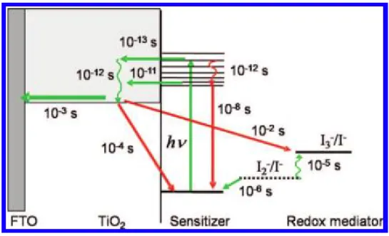
The electrolyte is employed to reduce the photo excited sensitizer and is subsequently reduced at platinum electrode. An effective electrolyte needs to have its reduction potential somewhere in between the work function of platinum and the ground state of the dye molecule, so that it can produce a driving force electron transfer within the DSSC. The most commonly used electrolyte for N3 and N719 is the iodide/tri-iodide complex in acetonitrile. By adding guanidinium thiocyanate to the electrolyte, the coulombic interactions between molecules are screened. Besides having the appropriate reduction potential, the iodide/tri-iodide based electrolyte can also slow down the recombination at the interface of the semiconductor. The time constants under working conditions are shown in Figure 2-21 for a Ru-dye-based solar cell using iodide/tri-iodide as the electrolyte.69 The reactions in a working dye-sensitized solar cell can be described as follows.
Ru(II) Ru(II)* photon absorption at sensitizer 2-11
Ru(II)* Ru(III)++ e- electron injected into TiO2 2-12
2 Ru(III)+ + 3I−2 Ru(II)- +I3− photo-excited sensitizer reduced by electrolyte
2-23
I3−+3e 3I− electrolyte reduced at Pt electrode 2-14
41
Ru(II)* Ru(II) relaxation 2-15
Ru(III)++ e- Ru(II) recombination 2-16
Figure 2-21. Overview of the time constants for the processes in a working dye-sensitized solar cell.69
42
complex will eventually decompose in the liquid electrolyte under UV irradiation or in a high temperature environment. Decomposition of the iodide/tri-iodide complex limits the practical application of the liquid electrolyte based DSSC. Thus, solid state dye-sensitized solar cells have been developed to overcome this problem. Because of the slow electron transfer in the polymer electrolyte, the reduction reaction between photo-excited sensitizer and electrolyte also slows down and the recombination rate is increased. Moreover, it is also difficult for the polymer electrolyte to fill the porous semiconductor film to obtain the largest surface area. So far, the solid state DSSC is still not able to achieve the same efficiency as the liquid based dye-sensitized solar cell.
43 Figure 2-22. The electron configuration in the DSSC.15
44
drop at some thickness.168-170 One explanation for this effect is that after all the photons in the absorption range of the dye are absorbed, the thicker porous film just creates more unnecessary interfaces between the semiconductor and the electrolyte, which increase the recombination rate and cause the solar cell efficiency to decrease. In a well-fabricated dye-sensitized solar cell, the TiO2 layer should not exceed 14 𝜇𝑚. Other metal oxides, such as ZnO,171, 172 Nb2O5,173, 174 and ZrO2,175 have been studied as photoanodes in DSSC. But so far, none can effectively compete with the TiO2 nanoparticle film.
By adding another scattering layer above the TiO2 nanoparticle film to increase the optical path in the solar cell, the highest overall efficiency of a DSSC using Ru-based dye has been reported, reaching 11.1% efficiency under AM 1.5 G simulated sunlight.176 To obtain the highest efficiency, the electrolyte solution used is dimethyl propylimidazolium iodide (0.6 M), lithium iodide (0.1 M), iodine (0.05 M), and tert-butylpryidine (0.5 M) in acetonitrile. A double layer of TiO2 was deposited on FTO using the screen printing method and sensitized with black dye. The results of the solar cell measurements showed short circuit current density JSC = 20.9 mA/cm2; open circuit voltage VOC = 736 mV; fill factor FF = 0.72; overall efficiency is 11.1%. The result was confirmed by National Institute of Advanced Industrial Science and Technology in Japan. The newest study reported a 12.3% overall efficiency by using a cobalt-based dye.14
2.3.2. Characterization techniques for solar cell
45
current source. When no light is illuminating the cell, the solar cell behaves like a diode. As the intensity of incident light increases, the solar cell generates a large photo-current.
Figure 2-23. I-V curve of a typical dye-sensitized solar cell.
In an ideal solar cell, the photo-current is defined as the difference between the current under illumination and the current in dark as shown in the following equation, which describes the solar cell’s capability of converting photons to electricity,
I = Il−Id = Il−I0�e qV
46
where 𝐼𝑙 is the photo-current generated under the illumination, 𝐼0 is the saturation current of the diode, q is the charge of an electron, k is the Boltzmann constant, T is the working temperature, V is the applied bias voltage on the solar cell.
For a real solar cell, the I-V curve suggests a more complicated model than a simple diode.177 Two resistors were brought into the new model as shown in Figure 2-24
Figure 2-24. The modified equivalent circuit for a working solar cell.
where Rseries is the internal equivalent series resistance of the solar cell, and Rshunt is the internal equivalent shunt resistance of the solar cell. Rseries andRshunt determine the fill factors of solar cells. After adding two resistors to the model, the new equation to describe I-V curve of a working solar cell becomes the following,
I = Il−Id = Il−I0�e
q�V+IRseries�
nkT −1� −V+IRseries
Rshunt . 2-18
47 Figure 2-25. Illuminated I-V sweep curve.
The short circuit current, also known as Isc, is defined as the photo generated current of a solar cell without any potential bias. It is calculated using following equation,
Isc= Il0− Id0 (when V = 0), 2-19
where Il0 is the current of a working solar cell under illumination without applied external voltage, and Id0 is the current of a solar cell in dark without applied external voltage.
48
Voc = V(when I = 0). 2-20
The output power of a solar cell can be estimated from the product of photo-current and bias voltage obtained from the I-V sweep curve. Pmax is defined as the maximum output power for solar cell.
The fill factor is a measure of the quality of solar cells, which is defined as the ratio between Pmax and the theoretical maximum power from the cell. It is typically in the range of 0.5 - 0.8.
Fill Factor =
PmaxIsc∙Voc
.
2-2149
Figure 2-26. Estimating series resistance and shunt resistance from I-V curve.
The efficiency of a solar cell is the ratio between the maximum output power for the solar cell and the power of the incident sunlight. It is calculated using the following equation
η
=
PmaxPin
=
Isc∙Voc∙ff
Pin
,
2-2250
Another measurement of the solar cell is the incident photon-to-current efficiency (IPCE), which is defined as the ratio between the number of photo-generated carriers and the number of incident photons. The IPCE value corresponds to the photo-current density of the solar cell under monochromatic illumination divided by the photon flux that strikes the cell. It can be calculated by measuring the photo-generated current under monochromatic illumination at each wavelength and the light intensity at that wavelength. IPCE describes the ability of converting photon to electricity at different wavelengths. The following equation is used to calculate IPCE
IPCE =Jsc(λ)
eϕ(λ)= 1240
Jsc(λ)[Acm−2]
λ [nm]Pin(λ)[Wcm−2], 2-23
where Jsc(λ) is the photo current density under illumination with light of wavelength λ,
Pin(λ) is the power of the incident light of wavelengthλ.
51
Hz), medium range (10-100 Hz) and low range (below 10 Hz) and measures the electrical properties of the Pt electrolyte interface at the counter electrode, the electrical properties of the semiconductor electrode electrolyte interface at the back electrode and the frequency response of the electrolyte, respectively. The small intercept on the Z’ axis measures the sheet resistance of the TCO electrode.
Figure 2-27. EIS measurent of a typical dye-sensitized solar cell.178 For a high performance DSSC, the large arc should be close to a circle and the internal resistance can be estimated from the diameters of these semi circles.
52
Figure 2-28. Equivalent circuit of dye-sensitized solar cell.178
By fitting the parameters in the equivalent circuit with the experimental data, the life time of electrons in semiconductor, the electron density in the semiconductor’s conduction band and the total number of electrons in the semiconductor’s conduction band can be estimated. Electrochemical impedance spectroscopy is a powerful tool to study the characteristics of the dye-sensitized solar cell at its working condition.
2.3.3. Flexible dye-sensitized solar cell
53
compression method.189 The highest efficiency of plastic-substrate dye-sensitized solar cells documented so far is 8%.190
2.3.4. Nanowire based dye-sensitized solar cells
The term “nanowire” describes the fact that the material shares the particular structure of being several microns long and sub 100 nm in diameter. A Nanowire array is considered as a candidate structure for the electrode in solar cells because of two advantages: 1) large surface area; and 2) excellent electrical properties of single crystalline nanowires. In 2005, Law first reported a DSSC using a ZnO nanowire array as the photoanode, showing the potential application of nanowires for solar cells.26 The results indicated that the diffusion coefficient for a single ZnO nanowire is several orders of magnitude higher than in nanoparticle deposited film and the vertically grown nanowires have an ohmic contact with substrate, helping the excited electrons transfer from dye molecules to the front electrode.
54
Tan and co-workers managed to use a composite of nanowires and nanoparticles to achieve 8.7% overall efficiency, compared with 6% using a nanoparticle film alone.191 Feng reported a new method of growing a rutile TiO2 array directly on FTO glass. A solar cell using this material showed 5.02% overall efficiency.61 Liu also reported a 3% dye-sensitized solar cell using directly grown TiO2 nanowires.120
Because of the morphological advantage of vertically grown nanowires, a highly foldable dye-sensitized solar cell was built using ZnO nanowires.145 Even though the efficiency was reported to be low, the study demonstrates the potential to build a highly flexible solar cell using aligned nanowires.
Figure 2-30. Schematic demonstrates the advantage of using nanowires as photoanode for a flexible dye-sensitized solar cell.145
2.4. Summary
55
56
Another challenge of nanowire synthesis is morphology control, which is the key to increasing surface area and to enhancing the performance of the solar cell.
CHAPTER 3
SYNTHESIS AND CHARACTERIZATION OF FLEXIBLE FREE-STANDING TiO2 NANOROD FILM
3.1. Synthesis of free-standing TiO2 nanowires film
58
Figure 3-1. Schematic diagram of the hydrothermal synthesis of TiO2 nanowire film.
59
Figure 3-2. a) The 1 cm by 2 cm free-standing film is folded and placed on a page of yellow paper with nanowires facing outside. b) The free-standing film is placed on a blue UNC logo print. It shows the semitransparency of the white film.
At the end of synthesis, the FTO layer was observed to have been damaged under high temperature and high pressure conditions. The electrical conductivity of the FTO layer was reduced to zero (measured using a four-probe method with Keithley 4200-SCS Semiconductor Characterization System).
3.2. Characterizations of TiO2 nanowires on FTO and free-standing film
3.3.1. Morphology of TiO2 nanowires
60
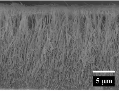
Microscope). Cross sectional images of TiO2 nanowires showed that the nanowires were highly aligned and grown on the FTO substrate. The nanowire layer has a uniform thickness across the substrate. The typical length of the nanowires is around 5 𝜇𝑚 and the diameter of nanowires is 50-100 nm as shown in Figure 3-3.
Figure 3-3. TiO2 nanowires grown at 150℃ for 4 hours: a) cross section of TiO2 nanowires grown on FTO, b) top view of nanowires.
61
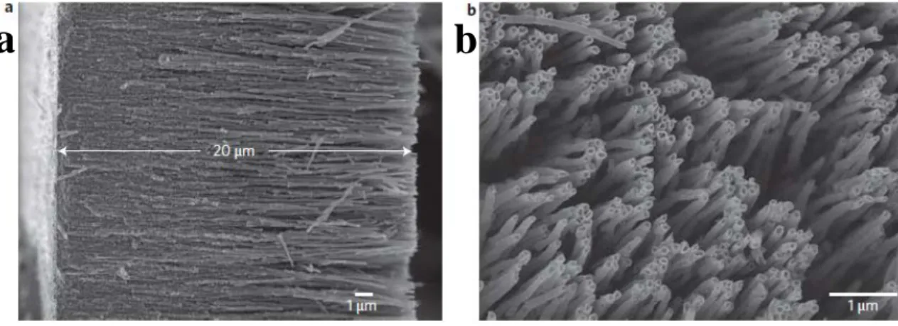
peeled off from FTO glass easily after 4 hour growth. The morphology of this layer was examined in SEM. The product is composed of a compact TiO2 layer with a nanowire layer on the top of the product. The total thickness of the film can reach up to 50 µm and the thickness of the nanowire layer is 3-5 𝜇𝑚 as shown in Figure 3-4.
Figure 3-4, SEM results of TiO2 layer using 3 ml titanium butoxide.
62
Figure 3-5. a) Cross sectional SEM image of the film, scale bar is 2.5 𝜇𝑚; b) Top view of the free-standing film, which is made of highly ordered nanowires, scale bar is 2 𝜇𝑚; c) bottom layer of the film, scale bar is 1 𝜇𝑚; d) folded film, scale bar is 50 𝜇𝑚.
3.3.2. X-Ray diffraction analysis of TiO2 nanowires grown on FTO
63
Figure 3-6. XRD spectrum of as grown TiO2 nanowires on FTO.
64
Figure 3-7. XRD spectrum from free-standing TiO2 film (Top) and the power sample prepared from film.
65
Figure 3-8. EDS spectrum from the back side of free-standing film.
3.3.3. TEM characterization of individual nanowire
Transmission electron microscopy (TEM) is a powerful tool to study the crystal structure and surface profile structures of materials, (especially for nanomaterials), which is able to provide atomic resolution and structural details. A JEOL 2010F was employed in this study. The JEOL 2010F has the capability of providing a point-to-point resolution of 0.25 nm and operating in many lens modes: HRTEM (high resolution transmission electron microscope), STEM (scanning transmission electron microscope), EDS (Energy-dispersive X-ray spectroscopy), NBED (nanobeam electron diffraction), and CBED (convergent beam electron diffraction). The crystal structure and the surface structure of the individual nanowires were studied using HRTEM images and nanobeam diffraction patterns.
66
67
Figure 3-9. HRTEM images and nanobeam diffraction pattern of an individual TiO2 nanowire.
3.3.4. Optical properties of free-standing TiO2 nanowires film
68
𝛼
𝑣∝
�ℎ𝜐−Egapℎ𝜐 3-1where 𝛼𝑣 is the absorption coefficient at light frequency 𝜐, ℎ𝜐 is the energy of incident photon and Egap is the band gap of semiconductor material. According to the absorption spectra and the fitting result, the band gap of TiO2 nanowires is obtained to be 3.12 eV, which is consistent with reported value for the rutile phase TiO2.
Figure 3-10. Absorption spectrum of rutile TiO2 film from both sides.
69
can help to reduce the reflection of the short wavelength light as shown in Figure 3-11. This is because the nanowire structure increases the optical path length in the film. The absorption in Figure 3-10 was calculated using the following equation,
Absorption=1-transimission-reflection. 3-2
Because TiO2 cannot absorb the light with wavelength longer than 400nm, 15 % long wavelength light (>400 nm) are caused by scattering the light through the side of the film.
Figure 3-11. Comparisons of transmission, reflection and absorption spectrum from both sides of TiO2 thin film.
3.3. Growth mechanism of TiO2 free-standing film
70
37.5% hydrochloric acid. The morphologies of TiO2 nanowires with different growth time were examined in SEM as shown in Figure 3-12.
Figure 3-12. Cross section of TiO2 nanowires grown on FTO with different growth times.
71
nanowire array steadily increases; after 6 hours growth, the thickness of film stop increasing, because titanium precursors in the solution are used up.
72
Figure 3-14. Topview SEM images of TiO2 nanowire grown on FTO with different growth time.
73
Table 3-1. Sheet resistance of FTO after different time length growth
Growth time (hour) 2 3 4 6
FTO substrate sheet
resistance (Ω) 13.39 Ω
13.53 Ω
13. 55 Ω
13 .6Ω
Figure 3-15. Schematic diagram of free-standing film growth mechanism: first, TiO2 nanowires start to grow from nuclei on FTO in the autoclave; and short randomly oriented nanowires are then obtained; these nanorods keep growing and stop when they reach their neighbors. The dense short TiO2 rods layer is formed. It is under the nanowires. Once the titanium precursor runs out, nanowires film stops growing. In a high temperature environment, the acid etches the FTO layer through the porous TiO2 nanorods layer. A white film can be peeled off from the substrate.
74