Optimization, Analysis and Comparison of Two
Stage and Three Stage Operational Amplifiers
using 0.3µm Process Technology for SCMOS
Arpita Johari Dr. Minal Saxena
Research Scholar Professor
Department of Electronics & Communication Engineering Department of Electronics & Communication Engineering Sagar Institute of Research & Technology Bhopal, India Sagar Institute of Research & Technology Bhopal, India
Abstract
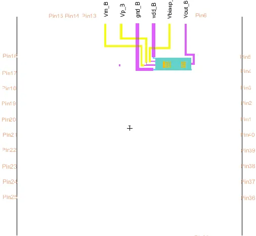
A Design presented in this work is a two stage and three stage or multistage CMOS operational amplifiers and frequency analysis of the same is also done and analyze the effect of various parameters on the characteristics of operational amplifier, which operates at 5V power supply using C5 process CMOS technology. Here parameters are computed and response curves are computed between all characteristics such as Gain, PM, GBW, Slew Rate etc using AC, DC and transient characteristics of it. The operational amplifier, design is a two-stage, three-stage, multi-stage CMOS operational amplifier. The design and simulations are carried out to achieve these values approximately. Design will be carried out in Electric CAD and LTSpice. Simulation results are verified using LTSpice. There is numerous numbers of configurations for operational amplifier exists in literature. The classification of the namely existing topologies includes single stage, two stage, three stage and multistage amplifiers. A Pad frame is also designed for a three stage topology operational amplifier DRCs and network consistency checks verified through the design using 300 nm for SCMOS. By results and reasons two stage and three stage topologies are suitable choices for low voltage and high performance applications. The presented architecture will also define the operating characteristics of Operational Amplifiers; a brief comparison is also presented for operating point analysis for multiple stage operational amplifiers. FFT analysis is also done for better noise index results.
Keywords: Operational Amplifiers, CMOS, Quiscent Point analysis, Operating Point, AC and DC analysis
________________________________________________________________________________________________________
I. INTRODUCTION
Operational Amplifiers are one of the most widely used building blocks for analog and mixed-signal systems. They are employed from dc bias applications to high speed amplifiers and filters. General purpose op amps can be used as buffers, summers, integrators, differentiators, comparators, negative impedance converters, and many other applications. With the quick improvements of computer aided design (CAD) tools, advancements of semiconductor modeling, steady miniaturization of transistor scaling, and the progress of fabrication processes, the integrated circuit market is growing rapidly. Nowadays, complementary metal-oxide semiconductor SCMOS technology has become dominant over bipolar technology for analog circuit design in a mixed-signal system due to the industry trend of applying standard process technologies to implement both analog circuits and digital circuits on the same chip. While many digital circuits can be adapted to a smaller device level with a smaller power supply, most existing analog circuitry requires considerable change or even a redesign to accomplish the same feat. With transistor length being scaled down to a few tens of nanometers, analog circuits are becoming increasingly more difficult to improve upon.. In particular, it has proved difficult to match the open loop gain of bipolar op amps with CMOS technology [3, 4]. This is due to the inherently lower transconductance of CMOS devices as well as the gain reduction due to short channel effects that come into play for submicron CMOS processes.
II. CMOS OPERATIONAL AMPLIFIER
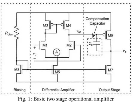
Fig. 1: Basic two stage operational amplifier
The differential amplifier offers a variety of advantages and is always used as the input to the overall amplifier. Since it provides common-mode rejection, it eliminates noise common on both inputs, while at the same time amplifying any differences between the inputs.etc.
Fig. 2: Block Diagram of a generic amplifier
The limit for which this common mode rejection occurs is called common-mode range and signifies the upper and lower common mode signal values for which the devices in the diff-amp are saturated. The differential amplifier also provides gain. The gain stage is typically a common-source or cascade type amplifier. So that the amplifier is stable, a compensation network is used to intentionally lower the gain at higher frequencies. The output stage provides high current driving capability for either driving large capacitive or resistive loads. The output stage typically will have low output impedance and high signal swing characteristics. In some cases, it may be advantageous to add bipolar devices to improve the performance of the circuitry. These will be presented as the multi stage opamp circuits are analysed.
III. MULTIPLE STAGE OPERATIONAL AMPLIFIERS
Figure 3 Schematic for two stage operational amplifier
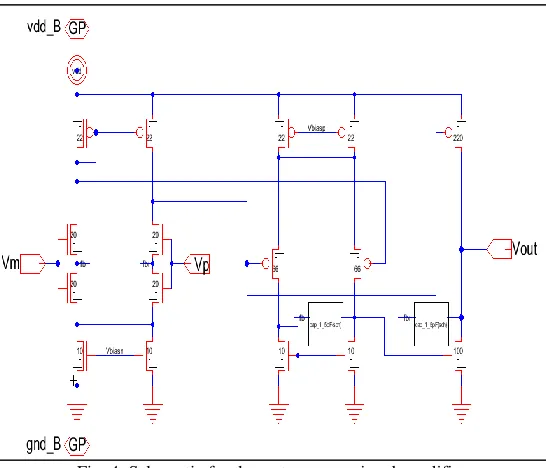
Fig. 4: Schematic for three stage operational amplifier
As this stage uses differential input unbalanced output differential amplifier, so it provide required extra gain. The bias circuit is provided to establish the proper operating point for each transistor in its saturation region.
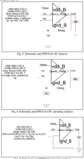
Fig. 5: Schematic and SPICE for AC analysis
Fig. 6: Schematic and SPICE for DC operating analysis
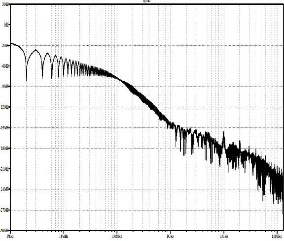
Fig. 8: AC Plot for multistage operational amplifier for 100 Hz to 100 GHz
Fig. 9: Snapshot of Operating Point for multistage SCMOS Operational Amplifier
FFT Index is done as follows for 3 stage Operational amplifier and is as shown below in figure 11
Table – 2
Table enlisting Frequency, Magnitude, Phase and Group Delay two stage SCMOS Operational Amplifier S.No. Frequency Magnitude Phase Group Delay
1. 1MHz --86.207dB 345.40° 55.021 ns 2. 10 MHz -84..88 dB 164.55° -146.52 ns 3. 100 MHz -124.82 dB -2.071° -76.89 ns 4. 1 GHz -161.29 dB -1.65° 924.655ns 5. 10GHz -207.39 dB -1.95° 856.84 ns 6. 25 GHz -217.83 dB -359.04° -99.69 ns
Table – 3
Table enlisting Frequency, Magnitude, Phase and Group Delay, multistage SCMOS Operational Amplifier S.No. Frequency Magnitude Phase Group Delay
1. 1MHz -26.942 dB -164.36° -157.98 ns 2. 10 MHz -71.027 dB 15.88° -39.72 ns 3. 100 MHz -77.85 dB 9.38 ° -130.78 ns 4. 1 GHz -143.60 dB 16.36° 188.15ns 5. 10GHz -159.9 dB -110.32° -46.64 ns 6. 25 GHz -189.91 dB 9.81° 30.04 ns
Electronics and Communication Engineering, Sagar Institute of Research and Technology, Bhopal for her able guidance, valuable help, enthusiastic attitude and suggestions.
REFERENCES
[1] Dr. Soni Changlani, Ayoush Johari “Implementation , analysis and comparison of 2 stage and 3 stage and multistage Operational Amplifiers” CICN IEEE
Conference November 2014
[2] Perenzoni, Matteo, Luca Parmesan, and David Stoppa. "A robust, power-and area-efficient gm-control for low-noise operational amplifiers." Analog Integrated Circuits and Signal Processing 82.1 (2015): 209-216.
[3] Grassi, Marco, Jean-Michel Redoute, and Anna Richelli. "Increased EMI immunity in CMOS operational amplifiers using an integrated common-mode
cancellation circuit." Electromagnetic Compatibility (EMC), 2015 IEEE International Symposium on. IEEE, 2015.
[4] Tepwimonpetkun, Samattachai, Bhirawich Pholpoke, and Woradorn Wattanapanitch. "Graphical analysis and design of multistage operational amplifiers
with active feedback Miller compensation." International Journal of Circuit Theory and Applications (2015).
[5] Ohno, Yasuhiko, et al. "Maximum and minimum voltage sample and hold circuits employing operational amplifiers composed of polycrystalline silicon thin-film transistors." Future of Electron Devices, Kansai (IMFEDK), 2014 IEEE International Meeting for. IEEE, 2014.
[6] Vigraham, Baradwaj, Jayanth Kuppambatti, and Peter R. Kinget. "Switched-Mode Operational Amplifiers and Their Application to Continuous-Time
Filters in Nanoscale CMOS." Solid-State Circuits, IEEE Journal of 49.12 (2014): 2758-2772.
[7] Irom, Farokh, Shri G. Agarwal, and Mehran Amrbar. "Compendium of Single-Event Latchup and Total Ionizing Dose Test Results of Commercial and Radiation Tolerant Operational Amplifiers." Radiation Effects Data Workshop (REDW), 2014 IEEE. IEEE, 2014.
[8] Eschauzier, Rudy GH, and Johan Huijsing. Frequency compensation techniques for low-power operational amplifiers. Vol. 313. Springer Science &
Business Media, 2013.
[9] Ahuja, Bhupendra K. "An improved frequency compensation technique for CMOS operational amplifiers." Solid-State Circuits, IEEE Journal of 18.6:
629-633.
[10] Azmi, Nilofar, and D. Sunil Suresh. "DESIGN OF LOW POWER OPERATIONAL AMPLIFIER USING CMOS TECHNOLOGIES." immunity 2 (2014):
[11] Todani, R. I. S. H. I., and ASHIS KUMAR Mal. "Simulator based device sizing technique for operational amplifiers." WSEAS Trans. Circ. Syst 13.1 (2014): 11-28.
[12] Yamatoya, Yuki, Akira Hiroki, and Hirokazu Oda. "Macromodeling of operational amplifiers for overdrive circuit design." Future of Electron Devices, Kansai (IMFEDK), 2015 IEEE International Meeting for. IEEE, 2015.
[13] Cardoso, Guilherme S., et al. "Reliability Analysis of 0.5 µm CMOS Operational Amplifiers under TID Effects." Journal of Integrated Circuits and Systems
9.1 (2014): 70-79.
[14] Petrov, A. S., K. I. Tapero, and V. N. Ulimov. "Influence of temperature and dose rate on the degradation of BiCMOS operational amplifiers during total
ionizing dose testing." Microelectronics Reliability 54.9 (2014): 1745-1748.
[15] Cuong, Nguyen Duy, and Tran Xuan Minh. "Design of analog MRAS controllers using operational amplifiers for motion control systems." Information Science, Electronics and Electrical Engineering (ISEEE), 2014 International Conference on. Vol. 2. IEEE, 2014.
[16] Prokopenko, Nikolay N., et al. "The Advanced Circuitry of the Precision Super Capacitances Based on the Classical and Differential Difference Operational Amplifiers." Design and Diagnostics of Electronic Circuits & Systems (DDECS), 2015 IEEE 18th International Symposium on. IEEE, 2015. [17] Jothimurugan, R., et al. "Improved realization of canonical Chua's circuit with synthetic inductor using current feedback operational amplifiers."
AEU-International Journal of Electronics and Communications 68.5 (2014): 413-421.
[18] Kusuda, Yoshinori. "5.1 A 60V auto-zero and chopper operational amplifier with 800kHz interleaved clocks and input bias-current trimming." Solid-State
Circuits Conference-(ISSCC), 2015 IEEE International. IEEE, 2015.
[19] Bakerenkov, A. S., et al. "Radiation Degradation Modeling of Bipolar Operational Amplifier Input Offset Voltage in LTSpice IV." Applied Mechanics and
Materials. Vol. 565. 2014.
[20] Huijsing, Johan, Rudy J. van de Plassche, and Willy Sansen, eds. Analog circuit design: operational amplifiers, analog to digital convertors, analog computer aided design. Springer Science & Business Media, 2013.
[21] Sakurai, Satoshi, and Mohammed Ismail. Low-voltage CMOS operational amplifiers: Theory, Design and Implementation. Vol. 290. Springer Science &
Business Media, 2012.
[22] Nakhostin, M., et al. "Use of commercial operational amplifiers in a low cost multi-channel preamplifier system." Radiation Physics and Chemistry 85 (2013): 18-22.
[23] Gray, Paul R., and Robert G. Meyer. "MOS operational amplifier design-a tutorial overview." Solid-State Circuits, IEEE Journal of 17.6 (1982): 969-982.
[24] Lipka, B., and U. Kleine. "Design of a cascoded operational amplifier with high gain." Mixed Design of Integrated Circuits and Systems, 2007. MIXDES'07. 14th International Conference on. IEEE, 2007.
[28] Aininzadeh, H., Mohammad Danaie, and Reza Lotfi. "A low-power design methodology for single-stage operational amplifiers." Design and Test of Integrated Systems in Nanoscale Technology, 2006. DTIS 2006. International Conference on. IEEE, 2006.
[29] Peng, Mingsheng, et al. "A 1-V quasi rail-to-rail operational amplifier with a single input differential pair." Region 5 Technical Conference, 2007 IEEE.
IEEE, 2007.
[30] Schlogl, F., Horst Dietrich, and Horst Zimmermann. "High-gain high-speed operational amplifier in digital 120nm CMOS." SOC Conference, 2004. Proceedings. IEEE International. IEEE, 2004.
[31] Klinke, R., B. J. Hosticka, and H. Pfleiderer. "A very-high-slew-rate CMOS operational amplifier." Solid-State Circuits, IEEE Journal of 24.3 (1989):
744-746.
[32] Karanicolas, Andrew N., et al. "A high-frequency fully differential BiCMOS operational amplifier." Solid-State Circuits, IEEE Journal of 26.3 (1991):
203-208.
[33] Lipka, B., and U. Kleine. "Design of a cascoded operational amplifier with high gain." Mixed Design of Integrated Circuits and Systems, 2007. MIXDES'07. 14th International Conference on. IEEE, 2007.
[34] Holman, W. Timothy, and J. Alvin Connelly. "A compact low noise operational amplifier for a 1.2 μm digital CMOS technology." Solid-State Circuits,
IEEE Journal of 30.6 (1995): 710-714.
[35] Gulati, Kush, and Hae-Seung Lee. "A high-swing CMOS telescopic operational amplifier." Solid-State Circuits, IEEE Journal of 33.12 (1998): 2010-2019.
[36] Duque-Carrillo, J. Francisco, et al. "1-V rail-to-rail operational amplifiers in standard CMOS technology." Solid-State Circuits, IEEE Journal of 35.1 (2000): 33-44.
[37] Chaudhari, Haresh S., Nilesh D. Patel, and Jaydip H. Chaudhari. "Optimization and Simulation of Two Stage Operational Amplifier Using 180nm and 250nm Technology."
[38] Chaudhari, Haresh S., and Nilesh D. Patel. "Simulation Of Two Stage Operational Amplifier Using 250nm And 350nm Technology." International Journal
of Engineering 2.4 (2013).
[39] Randal E. Bryant, Kwang - TingCheng , Andrew B Kahang, Kurt Kreutzer, Wojciech Maly,Richard Newton, Lawerance Pileggi, Jan M Rabaey, Alberto Saniovanni- Vincentelli, “Limitations and Challenges of CAD Technology for CMOS VLSI”
[40] Boise state university online tutorials at http://cmosedu.com/cmos1/electric/electric.htm.
[41] VLSI Open Source CAD Tools http://www.vlsiacademy.org/open-source-cad-tools.html