Design of On-Chip Permutation Network with
Programmable Arbiter for application level
selection of arbitration scheme
M.Ravinder1, K.Hanuja2
P.G. Student, Department of Electronics and Communication Engineering, St.Martin’s Engineering College,
Hyderabad, Telangana, India1
Associate Professor, Department of Electronics and Communication Engineering, St.Martin’s Engineering College,
Hyderabad, Telangana, India2
ABSTRACT:This paper presents the guaranteed bandwidth design of a novel on-chip network to support guaranteed traffic permutation in multiprocessor system-on-chip applications. The proposed network employs a pipelined circuit-switching approach combined with a dynamic path-setup scheme under a multistage network topology. The dynamic path-setup scheme enables runtime path arrangement for arbitrary traffic permutations.In this, Three arbitrary schemes are proposed ,which are Fixed priority,Round Robbin,Weighted priority or Garunteed bandwidth scheme.
KEYWORDS:Guaranteed throughput, multistage interconnection network, network-on-chip, permutation network, pipelined circuit-switching,traffic permutation.
I. INTRODUCTION
A trend of multiprocessor system-on-chip (MPSoC) design being interconnected with on-chip networks is currently emerging for applications of parallel processing, scientific computing, and so on. Permutation traffic, a traffic pattern in which each input sends traffic to exactly one output and each output receives traffic from exactly one input, is one of the important traffic classes exhibited from on-chip multiprocessing applications. Standard permutations of traffic occur in general-purpose MPSoCs, for example, polynomial, sorting, and fast Fourier transform (FFT) computations cause shuffled permutation, whereas matrix transposes or corner-turn operations exhibit transposepermutation. Recently, application-specific MPSoCs targeting flexible Turbo/LDPC decoding have been developed, and they exhibit arbitrary and concurrent traffic permutations due to multi-mode and multi-standard feature. In addition, many of the MPSoC applications compute in real-time, therefore, guaranteeing throughput (i.e., data lossless, predictable latency, guaranteed bandwidth, and in-order delivery) is critical for such permutation traffics.
Reviewing on-chip permutation networks (supporting either full or partial permutation) with regard to their implementation shows that most the networks employ a packet-switching mechanism to deal with the conflict of permuted data .Their implementations either use first-input first-output (FIFO) queues for the conflicting data .or time-slot allocation in the overall system with the cost of more routing stages ,or a complex routing with a deflection technique that avoids buffering of the conflicting data . The choices of network design factors, i.e., topology, switching technique and the routing algorithm, have different impacts on the on-chip implementation.
Regarding the topology, regular direct topologies, such as mesh and torus are intuitively feasible for physical layout in a 2-D chip. On the contrary, the high wiring irregularity and the large router radix of indirect topologies such as Benes or Butterfly pose a challenge for physical implementation .However, an arbitrary permutation pattern with its intensive load on individual source-destination pairs stresses the regular topologies and that may lead to throughput degradation .In fact, indirect multistage topologies are preferred for on-chip traffic-permutation intensive applications . Regarding the switching technique, packet switching requires an excessive amount of on-chip power and area for the queuing buffers
(FIFOs) with pre-computed queuing depth at the switching nodes and/or network interfaces. Regarding the routing algorithm, the deflection routing is not energy-efficient due to the extra hops needed for deflected data transfer, compared to a minimal routing. Moreover, the deflection makes packet latency less predictable; hence, it is hard to guarantee the latency and the in-order delivery of data.
II.RELATEDWORK
A system on a chip or system on chip (SoC or SOC) is an integrated circuit (IC) that integrates all components of a computer or other electronic system into a single chip. It may contain digital, analog, mixed-signal, and often radio-frequency functions—all on a single chip substrate. SoCs are very common in the mobile electronics market because of their low power consumption. A typical application is in the area of embedded. The contrast with a microcontroller is one of degree. Microcontrollers typically have under 100 kB of RAM (often just a few kilobytes) and often really are single-chip- systems, whereas the term SoC is typically used for more powerful processors, capable of running software such as the desktop versions of Windows and Linux, which need external memory chips (flash, RAM) to be useful, and which are used with various external peripherals. In short, for larger systems, the term system on a chip is hyperbole, indicating technical direction more than reality: a high degree of chip integration, leading toward reduced manufacturing costs, and the production of smaller systems. Many interesting systems which are too complex to fit on just one chip built with a processor optimized for just one of the system's tasks. When it is not feasible to construct a SoC for a particular application, an alternative is a system in package (SiP) comprising a number of chips in a single package. In large volumes, SoC is believed to be more cost-effective than SiP since it increases the yield of the fabrication and because its packaging is simpler. System on chip can be found in many product categories ranging from consumer to industrial systems.
1.) Cell phones use several programmable processors to handle the signal processingand protocol tasks required by telephony. These architectures must be designed tooperate at very low-power levels provided by batteries.
2.) Telecommunications and networking use specialized systems –on-chips, such asnetwork processors, to handle the huge data rates presented by modern transmission equipment.
III.ON-CHIPNETWORKDESIGN
Fig 1. On-chip network topology with port addressing scheme.
As motivated in Section I, the key idea of proposed on-chip network design is based on a pipelined circuit-switching approach with a dynamic path-setup scheme supporting runtime path arrangement. Before mentioning the dynamic path-setup scheme, the network topology is first discussed. Then the designs of switching nodes are presented.
On chip permutation topology:
Clos network, a family of multistage networks, is applied to build scalable commercial multiprocessors with thousands of nodes in macro systems.A typical three-stage Clos network is defined as C(n,m,p) where n represents the number of inputs in each of p first-stage switches and m is the number of second-stage switches. In order to support a parallelism degree of 16 as in most practical MPSoCs ,we proposed C(4 4 4) to use as a topology for the designed network (see Fig. 1). This network has a rearrangeable property that can realize all possible permutations between its input and outputs.The choice of the three-stage Clos network with a modest number ofmiddle-stage switches is to minimize implementation cost, whereas it still enables a rearrangeable property for the network.
Fig 2.Switch-by-switch interconnection and path-diversity capacity.
Fig. 3. Common switch architecture.
Dynamic path setup to support path arguments:
As designed in this network, each input sends a probe containing a 4-bit output address to find an available path leading to the target output. During the search, the probe moves forwards when it finds a free link and moves backwards when it faces a blocked link. By means of non-repetitive movement, the probe finds an available path between the input and its corresponding idle output. The EBP-based path-setup scheme is designed with a set of probe routing algorithms as mentioned later in Fig. 4. The following example describes how the path setup works to find an available path by using the set of path diversity shown in Fig. 2. It is assumed that a probe from a source (e.g., an input of switch 01 ) is trying to set up a path to a target destination (e.g., an available output of switch 22). First, the probe will non-repetitively try paths through the second-stage switches in the order of 10=>11=>12=>13 Assuming that the link 01=>10is available, the probe first tries this link and (req=1)then arrives at switch 10.
• If link 10=>22 is available, the probe arrives at switch 22 and meets the target output. An ans=Ack then propagates back to the input to trigger the transfer phase.
• If link10=>22 is blocked, the probe will move back to switch 01 (ans=back)and link is released (req=0). From switch 01, the probe can then try the rest of idle links leading to the second-stage switches in the same manner. By means of moving back when facing blocked links and trying others, the probe can dynamically set up the path in runtime in a conflict-avoidance manner.
Arbiter are electronics device that allocate access to shared resources’ bus arbiter is a device used multimaster bus system to decide which bus master will be allowed to control the bus for each bus cycle. A memory arbiter is a device used in shared memory system. To decide for each memory cycle which cpu will be allowed to access that shared memory.
The ARBITER has two functions:
• First cross-connecting the AnsOuts and the ICs through the Grant bus.
• Second as a refer for the requests from the ICs. When an incoming probe arrives at an
input, the corresponding IC observes the output status through the Status bus, and requests the ARBITER to grant it access to the corresponding OC through the Request bus.
Proposed arbitrary scheme:
Fig.5 Arbiter
1.switching node design :
CROSSBAR is a 4_4 full-connecting matrix designed with output multiplexers. The ICs and the ARBITER are clocked with the rising and the falling edges of the clock, respectively. By this implementation, probing is dynamically processed by the switch in one clock cycle basis.
As denoted in Fig. 3, the control part of switches performs the dynamic EPB-based path setup, whereas the data part simply provides configured paths for guaranteed switched data. This meets the target of designing the circuit-switched switches to support EPB-based path setup in C(4 4 4)network.
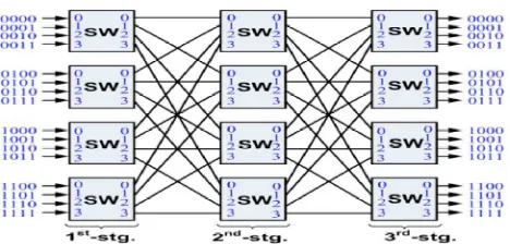
Fig.4. In order to support the probing path setup, ICs are implemented with different probe routing algorithms depending on its switch stage. The probe contains the 4-bit address of the destination,D3 D2 D1 D0 i.e.,(see Fig. 1 for the addressing scheme). The three routing algorithms for the switches in the first, the second, and the third stages are detailed in Fig. 4. In the first stage, the switch tries the free outputs in a non-repetitive manner (e.g., outputs0=>1=>2=>3=>4 ). This implementation avoids repetitively searching the same path that may result in a live-lock. The second- and third-stage switches rely on the two most significantD3 D2 bits and the two least signification bits D1 D0 of the destination address, respectively, to route the probe. As can be seen from Fig. 4, depending on the availability of the desired output or the feedback (i.e., the signal Ans) from the downstream switch, the IC in a given switch will change its FSM state and reply to the upstream switches accordingly.
To avoid a path setup interfering with others during the search and incurring a rearrangement of existing paths, a delay is set between the path setups launched one-by-one in a sequence in the test bench. This is to ensure that the previous path setup is completed before a new one is launched. As calculated based on the path-diversity graph shown in Fig. 2, the worst-case path setup needs 14 steps (hops) of moving its probe back and forth to search for a path. Each step of moving the probe needs two cycles, as derived from the cycle-accu rate design model. Hence, we set the delay to a value of 28 cycles (i.e.14 X 2) ,Arranging a full permutation requires 448 cycles to complete. By this setting, we simulate and validate the success of the design in arranging over ten different sets of 10 000 random full permutations.
2.Programmable arbiter:
In the previous design, the switch circuit consists of Arbiter as shown in above figure.This arbiter can be programmed and configurable with different arbitration schemes To overcome drawback in the previous system with arbitration schemes ,new design is proposed with new arbitration scheme for better efficiency.The previous schemes are itself are having drawbacks and these schemes are not suitable for all the real time applications.
The Arbitration schemes 1.Round Robin
2.Fixed Priority
2.1Round robin arbitration scheme:
It is one of the algorithms employed in computing in computer networks. In this scheme each task is assigned a fixed amount of time. The task has to finish within the allotted time otherwise the task should be completed in next round
Sometimes time is wasted in this scheme because of this efficiency is less. This scheme is suitable when all the tasks are having equal preference for each task. Round-robin scheduling is uncomplicated, easy to realize, and starvation-free.
2.2fixed priority arbitration scheme:
2.3 guaranteed band width scheme:
In this scheme, all tasks or devices will get access those who put request for grant to communicate with other device. By overcoming drawbacks of above two schemes, means inefficiency in round robin, starvation problem in fixed priority,this scheme provides better results so that the efficiency is increased.
For example, four devices are trying for accessing or communicate with other device. All devices has put request for grant. we first initially assign priorities. Initially the highest priority device gets access. what about other devices? Now the highest priority will get decreased by one value in next clock cycle or after getting first access. This process will continue until to the next highest priority value. Now the second highest priority device will get access. This process will continue to the next highest priority value and so on. In this all the devices will get access those devices put request for grant. So all the drawbacks are overcome and efficiency is increased.
Fig5.1.block diagram for gbw scheme
In this algorithm the highest priority gets decremented for each clock cycle until to the next highest Priority so that all the devices can access data. Starvation problem can be eliminated and maximum throughput is possible.
Fig5.2.FSM for Exhaustive profitable backtracking
IV. IMPLEMENTATION RESULTS
sized according to the requirements of real applications. A test chip comprised of 16 testing tiles is designed to test the network. Each testing tile has a 32-bit RISC and FIFO-based test wrappers interfaced with the proposed on-chip network. The RISC has 2 K IMEM, 2K DMEM, a GPIO, and a JTAG for programming and debugging. As seen in Fig. 5(a), the wrapper interfaces with the RISC system bus through a set of control and status registers. Due to the pre-configured circuit-switched data paths, applying a source-synchronous data transfer scheme is feasible. The 32 W 16 bit FIFO is used to log the test data transmitted from the source to the destination, and to support the source-synchronous transfer scheme. Fig. 5(b) details the source-source-synchronous transfer scheme, in which one wire of the data path is dedicated for source clock (strobe) transmission.
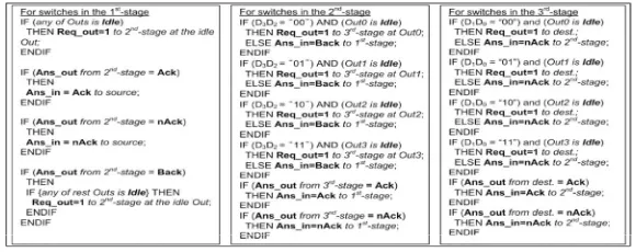
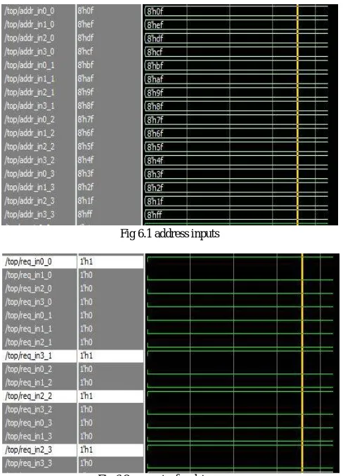
In multistage switching networks there are several stages are involved in real time for traffic permutations.These permutations are dynamically changes as per availability of path for connection. Here the network employs a 3x4 on chip switch network topology , each stage having four switches and each switch having four inputs. Any device from input side can send data to any device from output side. For example, any of four devices are wants communicate at output side at output side. For this we need put high request in signals. They has to appear at output pins those who put requests. The below figures shows simulation results.
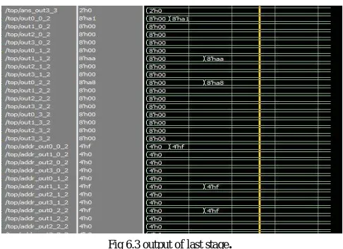
Fig 6.3 output of last stage
.
V. CONCLUSION
This paper has presented an on-chip network design supporting traffic permutations in MPSoC applications. By using a circuit-switching approach programmable arbiter and guaranteed bandwidth under a Clos network topology, the proposed design offers arbitrary traffic permutation in runtime with compact implementation overhead. A silicon-proven test-chip validates the proposed design and suggests availability for use as an on-chip infrastructure-IP supporting traffic permutation in future MPSoC researches.
REFERENCES
[1] S. Borkar, “Thousand core chips—A technology perspective,” in Proc. CM/IEEE Design Autom. Conf. (DAC), 2007, pp. 746–749.
[2] P.-H. Pham, P. Mau, and C. Kim, “A 64-PE folded-torus intra-chip communication fabric for guaranteed throughput in network-on-chip based applications,” in Proc. IEEE Custom Integr. Circuits Conf.(CICC), 2009, pp. 645–648.
[3] C. Neeb, M. J. Thul, and N.Wehn, “Network-on-chip-centric approach to interleaving in high throughput channel decoders,” in Proc. IEEE Int.Symp. Circuits Syst. (ISCAS), 2005, pp. 1766–1769.
[4] H. Moussa, A. Baghdadi, and M. Jezequel, “Binary de Bruijn on-chip network for a flexible multiprocessor LDPC decoder,” in Proc. ACM/ IEEE Design Autom. Conf. (DAC), 2008, pp. 429–434.
[5] H. Moussa, O. Muller, A. Baghdadi, and M. Jezequel, “Butterfly and Benes-based on-chip communication networks for multiprocessor turbo decoding,” in Proc. Design, Autom. Test in Euro. (DATE), 2007, pp. 654–659.
[6] S. R. Vangal, J. Howard, G. Ruhl, S. Dighe, H. Wilson, J. Tschanz, D. Finan, A. Singh, T. Jacob, S. Jain, V. Erraguntla, C. Roberts, Y. Hoskote, N. Borkar, and S. Borkar, “An 80-tile sub-100-w TeraFLOPS processor in 65-nm CMOS,” IEEE J. Solid-State Circuits, vol. 43, no. 1, pp. 29–41, Jan. 2008.
[7] W. J. Dally and B. Towles, Principles and Practices of Interconnection Networks:. San Francisco, CA: Morgan Kaufmann, 2004.
BIOGRAPHY
Ravinder (2014-2016):Persuing M.Tech in Embedded System Design from St.Martins Engineering College Affliated to Jawaharlal Nehru Technical University (JNTUH) Hyderabad.He completed his B.Tech in Electronics and Communication from Jagruthi Institute Of Engineering College(JNIT) Hyderabad.