Notice
While reasonable efforts have been made to assure the accuracy of this document, Motorola, Inc. assumes no liability resulting from any omissions in this document, or from the use of the information obtained therein. Motorola reserves the right to revise this document and to make changes from time to time in the content hereof without obligation of Motorola to notify any person of such revision or changes. No part of this material may be reproduced or copied in any tangible medium, or stored in a retrieval system, or transmitted in any form, or by any means, radio, electronic, mechanical, photocopying, recording or facsimile, or otherwise, without the prior written permission of Motorola, Inc.
It is possible that this publication may contain reference to, or information about Motorola products (machines and programs), programming, or services that are not announced in your country. Such references or information must not be construed to mean that Motorola intends to announce such Motorola products, programming, or services in your country.
Restricted Rights Legend
If the documentation contained herein is supplied, directly or indirectly, to the U.S. Government, the following notice shall apply unless otherwise agreed to in writing by Motorola, Inc.
Use, duplication, or disclosure by the Government is subject to restrictions as set forth in subparagraph (c)(1)(ii) of the Rights in Technical Data and Computer Software clause at DFARS 252.227-7013.
Preface
This document provides general information, hardware installation and
serviceability, operating instructions, and functional description for the Ultra Plus 603e, Ultra Plus 604, Ultra 603, Ultra 603e, and Ultra 604 PowerPCTM series of
motherboard platforms. It also includes general information and instructions for using the PPCBug debug Þrmware.
This document is intended for PC manufacturers, technical original equipment manufacturers (OEMs), and system integrators, who want to design OEM systems, supply additional capability to an existing PC-compatible system, or work in a lab environment for experimental purposes.
A basic knowledge of computers and digital logic is assumed.
To use this document, you may wish to become familiar with the publications listed in Appendix A, Related Documentation.
Document Conventions
The following conventions are used in this document: bold
is used for user input that you type just as it appears. Bold is also used for commands, options and arguments to commands, and names of programs, directories, and Þles.
italic
is used for names of variables to which you assign values. Italic is also used for comments in screen displays and examples.
courier
is used for system output (e.g., screen displays, reports), examples, and system prompts.
RETURN or <CR> or ENTER
represents the Return or Enter key.
CTRL
Document Terminology
Throughout this document, a convention has been maintained whereby data and address parameters are preceded by a character which speciÞes the numeric format, as follows:
For example, Ò12Ó is the decimal number twelve, and Ò$12Ó is the decimal number eighteen. Unless otherwise speciÞed, all address references are in hexadecimal throughout this document.
An asterisk (*) following the signal name for signals which are level significant denotes that the signal is true or valid when the signal is low.
An asterisk (*) following the signal name for signals which are edge significant denotes that the actions initiated by that signal occur on high to low transition. In this document, assertion and negation are used to specify forcing a signal to a particular state. In particular, assertion and assert refer to a signal that is active or true; negation and negate indicate a signal that is inactive or false. These terms are used independently of the voltage level (high or low) that they represent.
Data and address sizes are deÞned as follows:
A byte is eight bits, numbered 0 through 7, with bit 0 being the least significant.
A two-byte is 16 bits, numbered 0 through 15, with bit 0 being the least significant. For other RISC modules, this is called a half-word.
A four-byte is 32 bits, numbered 0 through 31, with bit 0 being the least significant. For the other RISC modules, this is called a word.
An eight-byte is 64 bits, numbered 0 through 63, with bit 0 being the least significant. For the other RISC modules, this is called a double-word.
The computer programs stored in the Read Only Memory of this device contain material copyrighted by Motorola Inc., Þrst published 1991, and may be used only under license such as the License for Computer Programs (Article 14) contained in MotorolaÕs Terms and Conditions of Sale, Rev. 1/79.
All Motorola PWBs (printed wiring boards) are manufactured by UL-recognized manufacturers, with a ßammability rating of 94V-0.
!
WARNINGThis equipment generates, uses, and can radiate electro-magnetic energy. It may cause or be susceptible to electro-magnetic
interference (EMI) if not installed and used in a cabinet with adequate EMI protection.
Motorola¨ and the Motorola symbol are registered trademarks of Motorola, Inc.
AIX¨, IBM¨, PC-ATª, PowerPC Architectureª, PowerPC 601¨, PowerPC 603ª, PowerPC 603eª, PowerPC 604ª, OS/2¨, PS/2¨, and RISCWatch¨ are trademarks or registered trademarks of International Business Machines Corporation.
PowerPCª is a trademark of International Business Machines Corporation, and is used by Motorola with permission.
DECchipª and Digitalª are trademarks of Digital Equipment Corporation.
Microsoft¨, Windowsª, and Windows NTª are trademarks or registered trademarks of Microsoft Corporation.
Super I/Oª is a trademark of National Semiconductor Corporation.
SNAPHATª and TIMEKEEPERª are trademarks of SGS-Thomson Microelectronics. All other products mentioned in this document are for identiÞcation purposes only and are trademarks or registered trademarks of their respective holders.
© Copyright Motorola, Inc. 1995, 1996 All Rights Reserved
European Notice: Board products with the CE marking comply with the EMC Directive (89/336/EEC). Compliance with this directive implies conformity to the following European Norms:
EN55022 (CISPR 22) Radio Frequency Interference
EN50082-1 (IEC801-2, IEC801-3, IEEC801-4) Electromagnetic Immunity The product also fulÞlls EN60950 (product safety) which is essentially the requirement for the Low Voltage Directive (73/23/EEC).
This board product was tested in a representative system to show
compliance with the above mentioned requirements. A proper installation in a CE-marked system will maintain the required EMC/safety
Contents
Introduction 1-1 Features 1-2 SpeciÞcations 1-3
Cooling Requirements 1-5 Regulatory Compliance 1-6 FCC Compliance 1-6 Equipment Required 1-7 Inter-Operability 1-8 Performance 1-8 Introduction 2-1 Before You Begin 2-1
Overview of Start-Up Procedures 2-3 Unpacking the Hardware 2-5
Field Replaceable Units 2-5 SIMM Memory Modules 2-7
Installing a SIMM 2-7 Removing a SIMM 2-8 Video DRAM Devices 2-8
Installing a Video DRAM Device 2-9 Removing a Video DRAM Device 2-9 Flash Memory Devices 2-9
Installing a Flash Device 2-10 Removing a Flash Device 2-10 Battery Backed NVRAM Devices 2-11 Riser and Cache Cards 2-11
Optional Internal Board Units 2-12 Riser Card 2-12
Installing and Removing a PCI or ISA Card 2-16 Installing a Riser Card 2-17
Removing a Riser Card 2-17 Cache Card 2-17
Installing a Cache Card 2-17 Removing a Cache Card 2-18 After Installing the Ultra System Board 2-19 Cooling Considerations 2-20
Parallel I/O Printer Port, J14 (Bottom) B-31 Ethernet 10base-T, J15 B-32
SVGA Graphics Port, J16 B-32 Keyboard Port, J17 B-33 Mouse Port, J18 B-33
Line Input Audio Jack, J19 B-34
Microphone Input Audio Jack, J20 B-34 Line Output Audio Jack, J21 B-34
SIMM Device Sockets, U3, U7, U11, U16 B-35 Flash Device Sockets, XU1 and XU2 B-37 Memory Maps B-39
Processor Memory Space B-39
Direct Mapped PCI Configuration Space B-41 ISA I/O Space Mapping B-42
PCI Space Mapping B-46 Interrupts B-46
PCI Interrupts B-46 ISA Interrupts B-47
List of Figures
User/Field Replaceable Components Location Diagram 2-6 SIMM Memory Module Outline 2-8
PCI/ISA Riser Card, 6-Slot 2-13 PCI/ISA Riser Card, 4-Slot 2-14 PCI Interrupt Routing 2-15 Cache Card 2-18
Controls and Indicators Location Diagram 3-3 System Board Block Diagram 4-2
Ethernet Block Diagram 4-8
System Board Audio System Diagram 4-13 PowerPC Debugger Architecture 5-4 Debug Monitor 5-5
List of Tables
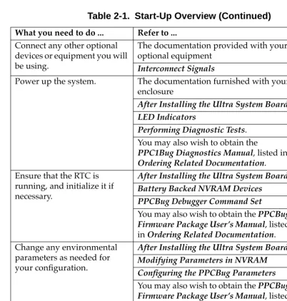
Ultra Plus and Ultra 60x Features 1-2 System Board SpeciÞcations 1-3 Start-Up Overview 2-3
Riser Card Types 2-12
System Board Memory with Various SIMM Sizes 4-4 MPC105 Memory Programming Assignments 4-4 Flash Device Compatibility 4-5
Minimum ROMFAL and ROMNAL Values 4-6 System Board Graphics Capability 4-9
Display Device Selection 5-6 Diagnostic Test Groups 5-21 Debugger Commands 6-8
1
1
General Information
Introduction
This manual describes the following Ultra family of PowerPC-based low profile form-factor motherboards: Ultra Plus 603e, Ultra Plus 604, Ultra 603, Ultra 603e, and Ultra 604.
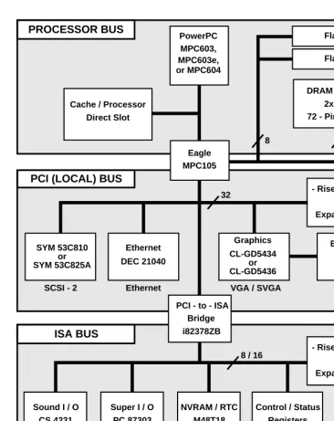
Unless otherwise specified, the Ultra Plus 603e and Ultra 604 motherboard platforms are referred to throughout this manual as Ultra Plus. The Ultra 603, Ultra 603e, and Ultra 604 motherboard platforms are referred to as the Ultra 60x. The Ultra Plusand the Ultra 60x are collectively referred to as the Ultra system board. The Ultra system board platform is an all-in-one motherboard implemented as a 9-inch by 13-inch single-plane printed circuit board. The system board allows for either an MPC603, MPC603e, or MPC604 RISC processor for the MPU (factory installed option) and an MPC105 PowerPC-to-PCI bridge as the memory controller between the processor bus (MPU) and the Peripheral Component Interconnect (PCI) bus. An Intel i82378ZB PCI-to-ISA bridge component (referred to as the PIB) allows Industry Standard Architecture (ISA) bus-compatible peripherals to be accessed by the MPC60x processor. The system board also provides for the addition of a riser card which supports PCI bus and/or ISA bus cards. Some of the standard PC (personal computer) interconnections that are included on the system board are two asynchronous serial ports, a parallel port, an IDE controller and connector, a floppy disk controller and connector, a keyboard, and a mouse.
In addition to the standard PC interconnections, the system board also provides a SCSI-2 PCI controller with standard connector, an Ethernet PCI controller with 10base-T RJ-45 connector and AUI DB15 connector, a Graphics PCI controller with SVGA connector, as well as business audio input/output capabilities, all on the primary motherboard.
General Information
1
The system board platform can be obtained as either a motherboard only, a motherboard integrated in a chassis, or a full computer system with motherboard, chassis, and peripherals.
Features
The following table describes the major features of the system board:
Table 1-1. Ultra Plus and Ultra 60x Features
Feature Description
Microprocessor Ultra Plus 603e MPC603e (@100 MHz)
Ultra Plus 604 MPC604 (@ 100 MHz or 133 MHz) RISC Ultra 603 MPC603 (@ 66 MHz)
Ultra 603e MPC603e (@100 MHz)
Ultra 604 MPC604 (@ 100 MHz or 133 MHz) RISC Bridge/memory
controller
MPC105 Eagle PowerPC-to-PCI bridge memory controller
Memory bus 64-bit + 8-bits parity, 66MHz local memory bus Cache Second-level cache/Processor Direct Slot (PDS)
Platform PowerPC Reference Platform (PRP) speciÞcation enabled
DRAM Four 72-pin SIMM sockets for 8 to 256 MB of DRAM (with or without parity)
I/O Ethernet (AUI, 10base-T) interface onboard SCSI-2 interface
onboard
Fast (Ultra 60x) Fast/Wide (Ultra Plus) Dual PC16550A asynchronous serial ports IEEE 1284 8-bit bidirectional parallel port Low/high-density ßoppy disk controller IDE hard-disk drive controller
VGA-compatible 8-bit color graphics system and SVGA, with onboard memory-expansion capability
Stereo 16-bit 44kHz business-class audio system
Specifications
1
Specifications
The specifications for the system board are listed in the following table.
Expansion slots PCI and ISA slot for either of two optional riser cards with PCI/ISA slots utilized as follows:
Six-slot card Five slots usable: Three PCI slots and two ISA slots, or two PCI slots and three ISA slots
Four-slot card Three slots usable: Two PCI slots and one ISA slot, or one PCI slot and two ISA slots
Indicators and switches
Onboard status LEDs and switches Provision for external connections Software
compatibility
Windows NT readiness AIX 4.1 readiness
Extensive diagnostics included
Table 1-2. System Board Specifications
Characteristics SpeciÞcations
Power Requirements (Exclusive of any attached peripheral devices)
MPC603 processor @ 66 MHz or
MPC603e processor @ 100 MHz
Maximum: 31 watts
+5 Vdc (± 5%), 3 A (typical), 5 A (maximum) +12 Vdc (± 10%), 250 mA (typical), 500 mA (maximum)
-12 Vdc (± 10%), 5 mA (typical), 10 mA maximum) -5 Vdc (± 5%), < 5 mA (maximum)
Table 1-1. Ultra Plus and Ultra 60x Features (Continued)
General Information
1
MPC604 processor @ 100 MHz or
MPC604 processor @ 133 MHz
Maximum: 43.5 watts
+5 Vdc (± 5%), 5.5 A (typical), 7.5 A (maximum) +12 Vdc (± 10%), 250 mA (typical), 500 mA (maximum)
-12 Vdc (± 10%), 5 mA (typical), 10 mA maximum) -5 Vdc (± 5%), < 5 mA (maximum)
Environmental
Temperature Operating 0û C to 50 û C at point of entry of forced air cooling Non-operating -40û C to 85û C
Altitude Operating 5,000 meters (16,405 feet) Non-operating 15,000 meters (49,215 feet) Relative humidity Operating 10% to 80% (non-condensing)
Non-operating 10% to 90% (non-condensing)
Physical Dimensions
Motherboard Height 1.375 inches (338.20 mm) (with connectors and slots only) 3.50 inches (88.90 mm)
(with connectors, slots, and add-in riser card and/or cache card)
Length 13 inches (330.0 mm) Width 9 inches (228.6 mm) Thickness 0.093 inch (2.36 mm)
Motherboard Rear Panel I/O Connectors
Ethernet interface AUI A 2-row, 15-pin, female DB-15 connector provides the AUI or 10base-2/10base-5 interface.
10base-T An RJ-45 connector provides the 10base-T interface. SCSI-2 interface A 50-pin header connector provides the Fast SCSI
interface.
A 68-pin header connector provides the Fast/Wide SCSI interface.
Serial port interface Two 9-pin connectors provide the EIA-232-D compliant serial port connection.
Table 1-2. System Board Specifications (Continued)
Specifications
1
Cooling Requirements
The system board is designed and tested to operate reliably with an incoming air temperature range from 0û to 50û C (32û to 122û F) with forced air cooling at a velocity typically achievable by using a 30 CFM (Cubic Feet/Minute) axial fan.
Temperature qualification is performed using a standard PC enclosure, with the system board unit under test simulated in a high power system configuration.
Test software is executed as the system board is subjected to ambient temperature variations. Case temperatures of critical, high power density integrated circuits are monitored to ensure
component vendorsÕ specifications are not exceeded.
Parallel port interface A 25-pin connector provides the standard IEEE 1284 parallel port connection.
Mouse interface A circular 6-pin mini-DIN connector provides the mouse interface with existing PS/2-type peripheral devices.
Keyboard interface A circular 6-pin mini-DIN connector provides the keyboard interface with existing PS/2-type peripheral devices.
Graphics interface A 3-row, 15-pin, female DB-15 connector provides the VGA-compatible graphics interface.
Audio interface Microphone A mini-stereo jack connector provides the external sound capture interface.
Audio output A mini-stereo jack connector provides the audio transfer to external recording devices, headphones, or ampliÞer speakers.
Audio input A mini-stereo jack connector provides the external sound capture from playback devices interface. Table 1-2. System Board Specifications (Continued)
While the exact amount of airflow required for cooling depends on the ambient air temperature and the type, number, and location of components, and other heat sources; adequate cooling for the motherboard low power components is achieved with an airflow of 100 LFM (Linear Feet/Minute).
Adequate cooling for the critical components (the microprocessors) requires an airflow of 200 LFM for the MPC603/MPC603e
processor with no heat sink, and an airflow of 250 LFM for the MPC604 processor with the current heat sink.
Regulatory Compliance
The system board is a board level product and will be used in several markets, including OEM sales for using in
industry-standard chassis. For those chassis not manufactured by Motorola, it is the responsibility of the OEM to meet the regulatory guidelines as determined by intended application. All external I/O connectors are shielded to aid in meeting EMI emissions standards.
The system board will be tested in a MCG chassis for EMI evaluation.
FCC Compliance
The system board is intended for use in systems meeting the following EMI/RFI regulations:
US FCC Class B
Canada DOC Class B
Equipment Required
1
Equipment Required
The following equipment is required to make a complete system: 2 4 MB SIMMs (or more; at least 16 MB is
recommended for NT)
1 Boot Flash device
1 SCSI and/or IDE hard disk and/or ßoppy disk 1 PC-type power supply or equivalent,
Inter-Operability
The system board will inter-operate with the following boards. PCI-compatible cards
ISA-compatible cards
Performance
The performance of the system board is based on the MPC60x RISC processor, the MPC105 PowerPC-to-PCI bridge/memory
controller, the speed of the installed memory devices, and the associated peripheral devices on the PCI (local) bus and the ISA bus.
!
Caution2
2
Preparing and Installing
the Ultra System Board
Introduction
The Ultra system board is primarily an all-in-one motherboard implemented on a 9-inch by 13-inch single-plane printed circuit board. The system board provides for the installation of several user-changeable components to enhance system features. In addition, the system board provides for the installation of several types of internal support or ÒdaughterÓ boards/cards, such as a riser card that supports PCI bus and/or ISA bus cards and a secondary cache card that supports additional cache memory.
Before You Begin
Before making any attempt to install your system board or replace or insert any add-on modules, cards, or components, make sure to turn all equipment power OFF and disconnect the power cable from the power source.
!
Warning
Dangerous voltages, capable of causing extreme injury or death, are present in this equipment. Use extreme caution when handling, testing, or adjusting modules, add-on cards, or components on the system board.
!
Caution2
Motorola strongly recommends that you use an antistatic wrist strap and a conductive foam pad when installing or upgrading the system. Electronic components, such as disk drives, computer boards, and memory modules, can be extremely sensitive to ESD. After removing the component from the system or its protective wrapper, place the component flat on a grounded, static-free surface, and in the case of a board, component-side up. Do not slide the component over any surface.If an ESD station is not available, you can avoid damage resulting from ESD by wearing an antistatic wrist strap (available at
electronics stores) that is attached to an unpainted metal part of the system chassis.
Use ESD
Unpacking the Hardware
2
Unpacking the Hardware
Note If the shipping carton is damaged upon receipt, request that the carrier's agent be present during the unpacking and inspection of the equipment.
Unpack the equipment from the shipping carton. Refer to the packing list and verify that all items are present. Save the packing material for storing and reshipping of equipment.
!
CautionAvoid touching areas of integrated circuitry; static discharge can damage circuits.
Field Replaceable Units
The system board contains six types of user- or field-replaceable/ installable units. These devices range from multiple-pin IC
(integrated circuit) chips to more complex units such as component modules and boards/cards. These units are:
❏ SIMM memory modules (two or four)
❏ Graphics expansion video DRAM devices (two, optional) ❏ Flash memory devices (two, socketed)
❏ Battery-backed NVRAM battery/crystal housing unit (one) ❏ PCI/ISA riser card (one, several variations available) ❏ Cache memory card (one, 256 KB or 512 KB options)
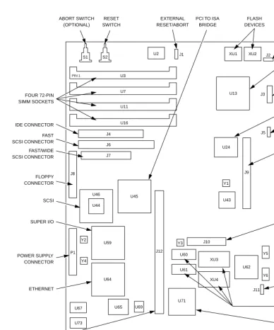
Refer to Figure 2-1 for the locations of the above components on the system board.
Field Replaceable Units
2
SIMM Memory Modules
The system board provides four tin-plated SIMM slots, labeled U3, U7, U11, and U16. The minimum number of SIMM modules required for operation is two. The total number of SIMM modules that the system board can hold is four. For proper operation, SIMM modules must be installed in pairs.
Note The system board uses SIMM (Single In-Line Memory Module) technology for implementing DRAM
memory. The system board can only be populated with either 32-bit or 36-bit (with parity) 72-pin SIMM memory modules.
Installing a SIMM
1. Turn the power off and disconnect the power cable from the power source.
2. All SIMMs, regardless of memory size, have a notch on one side of the connector finger section. This side notch denotes connector pin 1 (refer to Figure 2-2). Pin 1 on each SIMM slot is located toward the edge of the motherboard.
With the motherboard in the horizontal position, align pin 1 on the SIMM with pin 1 on the slot and carefully slide the SIMM module into the slot, noting that the SIMM module will be at a slight angle as it enters and sits in the slot. Be sure the SIMM module is seated properly.
Firmly press the SIMM memory module backwards until the left and right lock pins on the slot move outwards and then snap back inwards.
The SIMM is now securely in place.
2
Removing a SIMM1. Turn the power off and disconnect the power cable from the power source.
2. Simultaneously push the left and right lock pins on the slot outwards. The SIMM module releases and snaps forward. Pull the SIMM module out.
3. Reconnect the power cable to the power source and turn the power on.
For additional information on SIMMs, refer to the Memory Controller section in the Functional Description chapter.
Figure 2-2. SIMM Memory Module Outline
Video DRAM Devices
The system board provides two sockets, labeled XU3 and XU4, for the installation of additional video DRAM devices.
The system board is manufactured with 1 MB of video DRAM and can display graphics at a resolution of 1024 x 768 at 256 colors. The system board can also display graphics at a higher resolution of 1280 x 1024 at 256 colors with the addition of another 1 MB of video DRAM.
PIN 1
Field Replaceable Units
2
!
CautionThe DRAM component is a 40-pin integrated circuit chip; care should be taken not to damage the device pins.
Installing a Video DRAM Device
1. Turn the power off and disconnect the power cable from the power source.
2. Carefully align pin 1 on the video DRAM chip with pin 1 on the 40-pin socket (refer to Figure 2-1 for location of the socket). Firmly press the video DRAM chip downward. The video DRAM chip should descend into the socket to be securely in place. Repeat the procedure for the other video DRAM chip.
3. Reconnect the power cable to the power source and turn the power on.
For more information on the video DRAM, refer to the Graphics Controller section in the Functional Description chapter.
Removing a Video DRAM Device
1. Turn the power off and disconnect the power cable from the power source.
2. Using an extractor tool appropriate to the 40-pin device, carefully extract the video DRAM chip from the socket. 3. Reconnect the power cable to the power source and turn the
power on.
Flash Memory Devices
2
!
CautionAs supplied, the two sockets hold Flash devices that contain bootstrap firmware. If these devices are removed or corrupted, your system will not boot. Replacement Flash devices must perform board initialization and boot capability.
The Flash devices also contain the PPCBug debugger firmware. If removed or corrupted, you will not be able to use the debugger command set.
!
CautionThe Flash component is a 32-pin integrated circuit chip; care should be taken not to damage the device pins.
Installing a Flash Device
1. Turn the power off and disconnect the power cable from the power source.
2. Carefully align pin 1 on the Flash device with pin 1 on the 32-pin socket. Firmly press the Flash device downward. The Flash device should descend into the socket to be securely installed.
3. Reconnect the power cable to the power source and turn the power on.
Removing a Flash Device
1. Turn the power off and disconnect the power cable from the power source.
2. Using a PLCC extractor tool appropriate to the 32-pin device, carefully extract the Flash device from the socket.
3. Reconnect the power cable to the power source and turn the power on.
Field Replaceable Units
2
Battery Backed NVRAM Devices
At least 8KB of non-volatile RAM memory is provided by the Ultra system board for data retention. Installation of this memory storage is done in the factory because of the surface mounting nature of the devices.
The real-time clock (RTC) portion of the NVRAM is part of a SNAPHAT housing (battery and crystal) which is replaceable. This housing mounts on top of the NVRAM and provides 10 years of clock operation in the absence of power. Currently, this housing is installed in the factory and is designed to be removed by service technicians due to the tooling required to remove the device. On some boards, the RTC may have been put in PowerSave mode at the factory before shipping. You use PPCBugÕs SET command can to see if the clock is running, and start it if it is not. The clock must be running before you can use the Ultra system board. Refer to the PPCBug Debugger Command Set in Chapter 6.
Riser and Cache Cards
2
Optional Internal Board Units
The system board may contain one or more internal ÒdaughterÓ boards/cards, to implement PCI and ISA slots and to add cache memory.
Riser Card
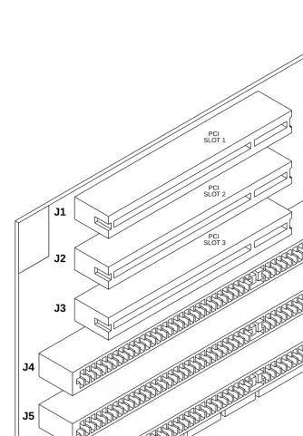
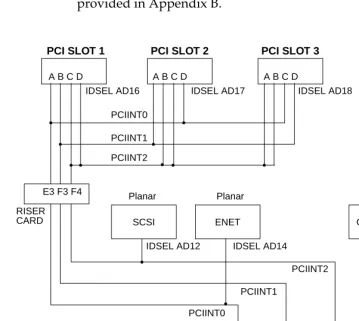
The optional riser card is inserted into the motherboardÕs riser card slot, labeled J12, and accepts the installation of third-party ISA or PCI bus cards. The riser cards currently available through Motorola include those listed in Table 2-1. They are pictured in Figures 2-3 and 2-4.
An IDSEL wired to each PCI slot determines the configuration address used to initialize the board upon power-up. Board
interrupts are routed to the interrupt controller on the Ultra system board. Details on connections and interrupt routing for PCI slots are provided in Appendix B.
Table 2-2. Riser Card Types
Motorola Part Number
Total Slots
PCI Slots
ISA Slots
Total Usable
Slots
Notes
MT-RISER 6 3 3 5 Of the two ÒmiddleÓ slots, you may use the PCI slot or the ISA slot, but not both.
Optional Internal Board Units
2
Figure 2-3. PCI/ISA Riser Card, 6-Slot
J1
J2
J3
J4
J5
J6
P1 PCI
SLOT 1
PCI SLOT 2
PCI SLOT 3
2
Figure 2-4. PCI/ISA Riser Card, 4-Slot
J4
J3
J2
J1
P1 PCI
SLOT 1
PCI SLOT 2
2
Installing and Removing a PCI or ISA Card!
CautionThis procedure assumes that the riser card is not yet connected to the motherboard.
6-Slot Card: You may insert up to three PCI cards and two ISA cards, or up to two PCI cards and three ISA cards into the connectors on the 6-slot riser card. The PCI cards are inserted component-side down into slots J1, J2, and/or J3 on the riser card, and the ISA cards are inserted component-side up into slots J6, J5, and/or J4. Note that slots J3 and J4 cannot both be used at the same time.
Note If using all three PCI slots, refer to the CAUTION in Chapter 1 under Performance.
1. To install a PCI or ISA card, align pin 1 on the PCI or ISA card with pin 1 of the appropriate PCI or ISA slot on the riser card (refer to Figure 2-3 for location of the PCI and ISA slots on the riser card). Firmly press the PCI or ISA card securely into the connector slot.
2. To remove a PCI or ISA card, hold it on opposite ends with both hands and pull up on it while rocking it from side to side. Continue until the unit works loose.
4-Slot Card: You may insert up to two PCI cards and one ISA card, or one PCI card and up to two ISA cards into the connectors on the 4-slot riser card. The PCI cards are inserted component-side down into slots J4 and/or J3 on the riser card, and the ISA cards are inserted component-side up into slots J1 and/or J2 on the riser card. Note that slots J2 and J3 cannot both be used at the same time.
1. To install a PCI or ISA card, align pin 1 on the PCI or ISA card with pin 1 of the appropriate PCI or ISA slot on the riser card (refer to Figure 2-4 for location of the PCI and ISA slots). Firmly press the PCI or ISA card securely into the connector slot.
Optional Internal Board Units
2
Installing a Riser Card
1. Turn the power off and disconnect the power cable from the power source.
2. Position the riser cardÕs P1 connector correctly above the socket (refer to Figure 2-1 for location of the riser socket). Firmly press the riser card down into the connector slot. The connector finger section of the riser card should completely descend into the connector slot to be securely installed. 3. Reconnect the power cable to the power source and turn the
power on.
Removing a Riser Card
1. Turn the power off and disconnect the power cable from the power source.
2. To remove the riser card, hold it on opposite ends with both hands and pull up on it while rocking it from side to side. Continue until the unit works loose.
3. Reconnect the power cable to the power source and turn the power on.
Cache Card
The system board may be enhanced with additional cache memory by using a cache board in the cache/PDS connector slot, labeled J9. The cache board is pictured in Figure 2-6.
The cache card may be populated (in the factory only) with various sizes of fast static RAM.
Installing a Cache Card
1. Turn the power off and disconnect the power cable from the power source.
2
socket). Firmly press the cache card securely into the connector slot and install the four screws provided.Figure 2-6. Cache Card
Removing a Cache Card
1. Turn the power off and disconnect the power cable from the power source.
2. Remove the four screws and hold the cache card on opposite ends with both hands. Pull up on it while rocking it from side to side. Continue until the unit works loose.
3. Reconnect the power cable to the power source and turn the power on.
PIN 1
After Installing the Ultra System Board
2
After Installing the Ultra System Board
The following paragraphs discuss what you will need to do after you have installed the Ultra system board into a chassis or an enclosure, as instructed in the documentation furnished with your chassis/enclosure. It assumes that you have installed or connected any optional devices or cards on the Ultra system board, and that you are using appropriate antistatic equipment. It also assumes that the Flash devices containing the PPCBug firmware are installed on the Ultra stem board.
1. Make sure that the power to the system is turned off. 1. If you intend to use PPCBug interactively, connect a video
monitor and keyboard to the SVGA port on the Ultra system
board, or connect a terminal to be used as the PPCBug system console to the COM1 port. If you are using COM1, set the
console terminal up as follows: Ð Eight bits per character Ð One stop bit per character Ð Parity disabled (no parity)
Ð Baud rate = 9600 baud (default baud rate of the port at power-up)
Refer to Display Device in Chapter 5.
2. Replace the chassis panels and/or covers and connect cables to peripheral devices as appropriate
3. Reconnect the system to the AC or DC power source, and turn the equipment power on. The Ultra system boardÕs PWR
LED will light.
4. Note that a set of confidence tests is run, and the debugger prompt PPC1-Bug> appears.
2
5. Use the SET command to verify that the RTC clock has been started. If not, set the date and time of day with the SETcommand. Refer to PPCBug Debugger Command Set in Chapter 6.
6. Use the CNFG and ENV commands to verify that the default configuration and environmental parameters are suitable and/or to customize your environment. Refer to Auto Boot, ROMboot, and Network Auto Boot in Chapter 5, and to Chapter 7, Advanced Debugger Topics.
7. Program the Ultra system board as desired. Refer to
Appendix B, Technical Data, and to the Ultra 603, Ultra 603e, and Ultra 604 ProgrammerÕs Reference Guide.
Cooling Considerations
A 3-pin header, labeled J5, is provided on the Ultra system board for powering a dedicated fan to supply the forced air cooling required.
!
CautionPosition is important; the air must blow across the MPU.
3
3
Using the Controls and
Indicators
Introduction
This chapter describes the control switches and indicators located on the Ultra system board. These devices are illustrated in the controls and indicators location diagram, Figure 3-1.
The system board may have one or two push-button switches (one is optional) and four LED (light-emitting diode) indicators. They are located adjacent to the SIMM sockets.
Control Switches
ABORT (S1)
When you press the ABORT push-button switch, it generates an interrupt request (IRQ8) to the Super I/O device. This can then be handled by software, usually to abort program execution.
Note The ABORT push-button switch may be optional on your system board.
RESET (S2)
3
LED Indicators
The four LED indicators located on the system board are: PWR, DSK, ENET, and BEAT.
PWR (DS1)
The green PWR LED is lit when +5V power is applied to the system board.
DSK (DS2)
The green DSK LED is lit when the BSY signal of the SCSI device is asserted or the IDE LED signal on the IDE connector is asserted by the IDE device.
ENET (DS3)
The yellow ENET LED is connected to the Ethernet device and indicates that Ethernet packets are being received when lit.
BEAT (DS4)
LED Indicators
3
Figure 3-1. Controls and Indicators Location Diagram
1579 9507 U11
U7 U3 S1 S2
U2
J1 XU1 XU2 J2
J3 U13
PWR RESET
SWITCH
DS1 DS2
DSK
DS3 DS4
ENET BEAT (OPTIONAL)
4
4
Functional Description
System Board Description
This chapter provides a block diagram level description of the Ultra system board. The functional description provides an overview of each of the major sections, grouped according to their locations on the processor bus, the PCI (local) bus, and the ISA bus. The block diagram shown in Figure 4-1 illustrates the general architecture of the system board.
Processor Bus
The system board contains the processor, memory, and all the associated peripheral and I/O controllers.
Microprocessor
The system board directly supports the MPC603, MPC603e, and MPC604 processors at speeds up to 100 MHz or more, where those speeds are supported by both the installed MPC60x processor and the MPC105 memory controller.
The restrictions are that the CPU bus speed may not exceed 66 MHz and the PCI bus speed may not exceed 33 MHz.
Processor Bus
4
Cache Memory/ PDS Slot
The MPC60x bus signals and the MPC105 chip cache-control signals, plus a few additional signals, are connected to a 190-pin connector. This allows the system board to accommodate a secondary cache board.
This slot may also be used to analyze critical signals using a specialized card and test equipment.
Memory Controller
The system board uses the MPC105 PowerPC-to-PCI
Bridge/Memory Controller chip to provide memory control, DRAM refresh, and memory decoding for banks of DRAM and/or Flash. The system board contains sockets or board locations to install any of the following memory devices:
❏ Dynamic RAM (72-pin SIMM DRAM modules) ❏ Flash device (electrically alterable)
❏ NVRAM (battery backed)
On the system board, the DRAM interface is connected to four 72-pin SIMM sockets. These may be populated with either 32-bit or 36-bit SIMM memory modules (the latter providing optionally-supported parity checking). This allows a maximum of 256 MB of memory on the system board. Table 4-1 shows how various sizes of memory may be installed in the system board using available SIMMs.
The MPC105 uses a 64-bit memory interface, so SIMMs must always be installed in multiples of two. Different sizes of SIMMs are allowed, as long as the pairs are of the same type, speed, and size. The system board senses the type and speed of installed SIMMs and can configure the MPC105 for the user-installed size and speed of memory automatically, via software.
4
Table 4-2 provides the MPC105 memory programming assignments for the memory banks on the system board.
Note Both sockets of a bank must be populated.
Table 4-1. System Board Memory with Various SIMM Sizes
SIMM Technology Quantity System Memory Size
1M x 32/36 2 8MB
4 16MB
2M x 32/36 2 16MB
4 32MB
4M x 32/36 2 32MB
4 64MB
8M x 32/36 2 64MB
4 128MB
16M x 32/36 2 128MB
4 256MB
Table 4-2. MPC105 Memory Programming Assignments
SIMM Bank Socket CAS# RAS# Data Bits
A
U3 0 - 3 0, 2 DH[0..31]
U7 4 - 7 0, 2 DL[0..31]
B
U11 0 - 3 1, 3 DH[0..31]
Processor Bus
4
Flash Devices
The system board provides two 32-pin sockets for Flash devices to provide up to 8 megabits of Flash storage. These devices may be used to store system boot-up software and Flash programming options needed for initial setup (before the Flash has been
programmed). These devices may also be used to store HAL code, etc.
Note The MPC105 specification refers to ROM access using a special 32-bit mode (which requires four ROMs or wide parts). This mode is not used on the system board. Instead, the Flash access method is used to access byte-wide devices. The MPC105 handles the interface to these devices transparently so software is not affected. The system board-compatible Flash device currently supported by Motorola is shown in the following table. These devices are supplied on the board and contain boot firmware. Refer to the cautions in Chapter 2 about modifying or removing these devices.
Under normal operation, the Flash devices are in Òread-onlyÓ mode, their contents are pre-defined, and they are protected against inadvertent writes due to loss of power conditions. However, for programming purposes, programming voltage is always supplied to the devices and the Flash contents may be modified by executing the proper program command sequence. Refer to the third-party data sheet for further device-specific information and/or to the PFLASH PPCBug command.
Table 4-3. Flash Device Compatibility
Type Size Organization Example
Part No. Notes
Peripheral Component Interconnect (PCI) Bus
4
PCI-to-ISA Bridge (PIB)
The PCI-to-ISA bridge component is the Intel i82378ZB (the ÒPIBÓ), which allows ISA-compatible peripherals to be accessed by the MPC60x processor. The PIB includes an 8-channel DMA controller for ISA devices, a timer, and a PCI/ISA interrupt controller. All PCI devices use the PIBÕs ISA interrupt controller to prioritize interrupts into the system processor.
Small Computer Systems Interface (SCSI)
The Ultra Plus system boards implement a SCSI-2 (Fast/Wide) interface using the SYM 53C825A, and the Ultra 60x system boards implement a SCSI-2 (Fast) interface using the SYM 53C810. These parts provide a SCSI interface compatible with X2.131-1986 (SCSI-1) and with X3.131-1990 (SCSI-2).
The system board contains active SCSI terminators which may be used when no internal SCSI devices are present yet external ones are desired; or with internal devices only. The terminators may be disabled under software control to eliminate the need for end-users to experiment with termination options.
Ethernet
4
Graphics Controller
The system board contains a VGA-compatible Cirrus graphics controller (the CL-GD5434 or CL-GD5436) which is capable of displaying graphics at resolutions of up to 1280 x 1024 at 256 colors, at refresh rates up to 87 Hz. The graphics subsystem may be equipped with either 1 MB or 2 MB of video DRAM; the extra DRAM is only needed for higher resolutions and is not installed for low-cost options. The system board comes equipped with sockets to allow users to install the extra memory when needed.
The GD5434 and GD5436 are programmable and can provide literally hundreds of different resolutions. The following table provides some of the more useful options.
Other features include:
❏ Internal power-save control
❏ VESA monitor power-save controls ❏ Expansion/replacement
❏ BitBLT engine (for faster rendering)
Figure 4-2. Ethernet Block Diagram DEC21040
Transformer
10base-T I/F 10base-T
System Board External
10base-5 10base-2 AUI
Transceiver RJ - 45
DB - 15 Ethernet
Industry Standard Architecture (ISA) Bus
4
Notes (1) The graphics hardware does not implement any byte-swapping hardware to resolve differences between Òlittle-endianÓoperating systems (such as Windows NT) and Òbig-endianÓ operating systems (such as AIX).
(2) A VESA Advanced Feature Connector (VAFC) is provided for connection of auxiliary devices.
Industry Standard Architecture (ISA) Bus
The system board implements a standard PC-type ISA bus operating at speeds up to 8.33 MHz. This bus is used for
inexpensive I/O controllers used on the system board as well as for allowing compatibility with the numerous ISA boards present in the PC market.
The following sections describe the various peripheral devices present on the ISA bus.
Table 4-5. System Board Graphics Capability
Width Height Colors Refresh
Rates (Hz) Interlaced?
Additional Memory
640 480 16, 256, 32K 60, 75 No None
640 480 16M 60 No None
800 600 16, 256, 32K 60, 75 No None
800 600 16M 60 No None
1024 768 16, 256, 64K 60, 70 No None
1024 768 16M 87 Yes None
1280 1024 16, 256 60 Hz No 1 MB
4
Super I/O (SIO) Controller
A large number of general-purpose I/O ports are provided through the National Semiconductor PC87303 ÒSuper I/OÓ (SIO) controller, including:
❏ Serial ports (two) ❏ Parallel port
❏ IDE (hard disk) interface ❏ Floppy-disk interface ❏ Keyboard interface ❏ Mouse Interface
The SIO chip includes several power-down options, and includes an automatic power-down controller for the floppy disk controller. The following sections detail the capabilities of the SIO chip.
Serial Ports
The SIO chip provides two EIA-232-D compliant DTE serial ports, at baud rates from 50 to 19,200 baud. The rear panel of the system board provides access to these two ports through two 9-pin DB male connectors. The serial ports are software and hardware compatible with the PC16450 and the PC16550A
(industry-standard serial controllers), including a 16-level FIFO buffer. These ports may also be used for Musical Instrument Digital Interface (MIDI) communications with the appropriate external buffers.
Parallel Port
The parallel port is compatible with IEEE standard 1284, including the Extended Capability Port (ECP) and Enhanced Parallel Port (EPP), as well as simple Centronics compatibility.
Industry Standard Architecture (ISA) Bus
4
Intelligent Device Expansion (IDE) Interface
A 40-pin male header is provided for the connection between the SIO chip and Intelligent Device Expansion (IDE) peripherals, such as hard disk or CD-ROM drives. The IDE interface conforms to the X3.221 revision 4.A AT Attachment specification (which covers the majority of IDE devices).
The IDE interface may be used with many types of low-cost disk drives, though only two IDE devices maximum are allowed on any IDE interface.
Floppy Disk Controller (FDC)
A low- and high-density MFM Floppy Disk Controller (FDC) is the standard FDC device on the system board. The controller is compatible with the industry-standard components previously used to implement floppy disk controllers: the DP8473, the 765A, and the N82077. Software designed to operate these devices may be used to control the FDC in the SIO chip without change.
The FDC may be used to support any of the following devices: ❏ 3.5Ó 1.44 MB floppy disk drive
❏ 5.25Ó 1.2 MB floppy disk drive
❏ Standard 250 kbps to 2 Mbps tape drive systems
A 34-pin male header provides the connection between the SIO chip and the floppy disk.
Keyboard/Mouse
Keyboard and mouse communication is provided by the PC87303. All electrical connections between the keyboard/mouse and the controller are filtered for RFI, as these devices are often a source of RFI. Additionally, the 5 volt power supplied to the mouse and keyboard are separately current-limited with a self-resetting fuse (also known as a ÒpolyswitchÓ).
4
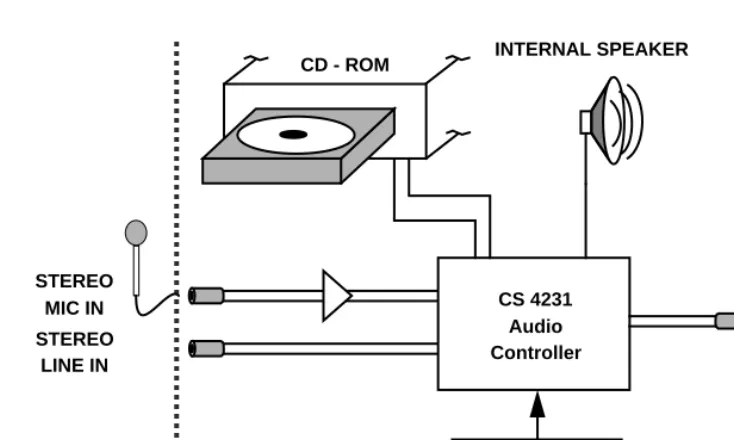
Audio Controller
The audio system is provided by the Crystal Semiconductor CS4231, a multimedia audio Coder/Decoder (CODEC). This device is capable of simultaneously recording and playing 16-bit stereo CD-quality audio samples. Both the recording and the playback subsystems feature a 16-level FIFO to allow the interrupt request rate to be minimized.
The CS4231 is compatible with the PowerPC Reference Platform (PRP) specification and with the Windows Sound System. The audio system of the system board has the following features:
❏ 16-bit stereo audio generation and capture ❏ MPC-compatible audio mixer
❏ Internal CD-ROM audio connection ❏ Full duplex stereo throughout
The general architecture of the audio system on the system board is shown in Figure 4-3.
Using the internal mixing and full duplex record/playback capabilities of the audio system, the following capabilities are possible, some simultaneously.
❏ Play CD-ROM to internal speaker, external speakers or headphones
❏ Record CD-ROM samples to disk
❏ Transfer human speech samples to system memory for recognition
❏ Play synthesized sounds/noises
Industry Standard Architecture (ISA) Bus
4
The Òbeep generatorÓ is provided by the PCI-to-ISA bridge
controller, and is a simple timer-based square-wave output. This is compatible with the simple sound present on PCs and may be used by system firmware without requiring much software support.
CD-ROM Audio Connection
The audio system contains two connectors which allow audio from CD-ROM drives to be amplified and driven through the audio amplifiers, allowing CD audio to be heard on the external
headphone or speaker connectors. The CD-ROM audio connector is configured so that it is compatible with most popular CD-ROM audio connectors. Custom audio cables allow other types of CD-ROM drives to be used as well.
Figure 4-3. System Board Audio System Diagram
SYSTEM BOARD
INTERNAL SPEAKER
Internal Beep Generator
STEREO LINE / HEADPHONE
OUT STEREO
MIC IN STEREO
LINE IN
CS 4231 Audio Controller CD - ROM
4
Non-Volatile RAM (NVRAM)
The system board provides 8KB of NVRAM storage for booting information, security passwords, etc. This is provided through the SGS-Thomson M48T18, a device that combines the RAM with a battery and a real-time clock. This memory is located on the 8-bit ISA bus through indirect access registers.
Real-Time Clock (RTC)
The real-time clock is a portion of the non-volatile RAM
5
5
PPCBug -- Getting Started
PPCBug Overview
The PPCBug firmware is the layer of software just above the hardware. The firmware provides the proper initialization for the devices on the PowerPC board or system upon power-up or reset. This chapter describes the basics of PPCBug and the architecture up to the point where the boot is done, and gives details on the different types of boot that are available: ROMboot, Auto Boot, and Network Auto Boot. Auto Boot is the default test configuration in the firmware.
Chapter 6 describes the monitor (interactive command portion of the firmware) in more detail, and gives more details on actually using the PPCBug debugger and the special commands. Chapter 6 also contains a complete list of PPCBug commands.
Chapter 7 contains information about the CNFG and ENV commands, system calls, and other advanced user topics.
PPCBug Basics
The PowerPC debug firmware, PPCBug, is a powerful evaluation and debugging tool for systems built around the Motorola
PowerPC microcomputers. Facilities are available for loading and executing user programs under complete operator control for system evaluation.
PPCBug provides a high degree of functionality, user friendliness, portability, and ease of maintenance
5
PPCBug includes commands for:
❏ Display and modification of memory ❏ Breakpoint and tracing capabilities
❏ A powerful assembler and disassembler useful for patching programs
❏ A self-test at power-up feature which verifies the integrity of the system
PPCBug consists of three parts:
❏ A command-driven, user-interactive softwaredebugger, described in the PPCBug Debugging PackageUserÕs Manual. It is hereafter referred to as Òthe debuggerÓ or ÒPPCBugÓ. ❏ A command-driven diagnostics package for the Ultra
hardware, hereafter referred to as Òthe diagnostics.Ó The diagnostics package is described in the PPC1Bug Diagnostics Manual.
❏ A user interface or debug/diagnostics monitor that accepts commands from the system console terminal.
When using PPCBug, you operate out of either the debugger directory or the diagnostic directory.
❏ If you are in the debugger directory, the debugger prompt
PPC1-Bug> is displayed and you have all of the debugger
commands at your disposal.
❏ If you are in the diagnostic directory, the diagnostic prompt
PPC1-Diag> is displayed and you have all of the diagnostic
commands at your disposal as well as all of the debugger commands.
PPCBug Implementation
5
causes execution of user target code (e.g., GO), then control may or may not return to PPCBug, depending on the outcome of the user program.
PPCBug Implementation
PPCBug is written largely in the C programming language, providing benefits of portability and maintainability. Where necessary, assembler has been used in the form of separately compiled program modules containing only assembler code. No mixed language modules are used.
Physically, PPCBug is contained in two Flash devices, providing 1MB of storage. The executable code is checksummed at every power-on or reset firmware entry. The result is checked with a pre-calculated checksum contained in the last 16-bit word of the Flash image.
Comparison with Other MCG Debuggers
PPCBug is similar to previous Motorola Computer Group (MCG) firmware debugging packages such as MVME147Bug,
MVME167Bug, and MVME187Bug, with differences due to microprocessor architectures. These differences are primarily reflected in the:
❏ Instruction mnemonics ❏ Register displays
5
Installation and Start-up
Power-Up/Reset Sequence
Figure 5-1 illustrates the basic flow the firmware follows at a power-up/reset sequence.
The default boot routine is Auto Boot. Using the ENV command (Chapter 7), you can select either ROMboot or Network Auto Boot as the boot mechanism.
Figure 5-1. PowerPC Debugger Architecture
STARTUP
INITIALIZATION
MONITOR BOOTING POST
Power-up/reset initialization
Initialize devices on the PowerPC board/system
Power On Self Test diagnostics
Firmware-configured boot mechanism; available choices are ROMboot, Auto Boot, or Network Auto Boot (default is Auto Boot)
Interactive, command-driven on-line PowerPC debugger (when ROMboot is chosen)
Installation and Start-up
5
Debug Monitor
The debug ÒmonitorÓ (interactive command level) is accessed after a ROMboot is done in the firmware. At the monitor, a number of different commands may be entered to interact with the hardware. Specifically, the commands are routed through character, disk, and network I/O drivers in the firmware (refer to Figure 5-2). This way the actual register settings and commands used by the devices are transparent to a firmware user. The firmware user only needs to be familiar with the basic PPCBug commands.
Figure 5-2. Debug Monitor
Display Device
The PPCBug firmware can be displayed either via the conventional mechanism of a console terminal connected to the serial port (COM1)
or it can be displayed on a video monitor connected to the SVGA
port.
The firmware checks for the presence of a connected keyboard, and for the presence of a connected mouse device. If either (or both) of these devices is connected to the system board and a firmware supported video monitor is found, the firmware is automatically brought up on the connected video monitor.
COMMAND SET
PowerPC HARDWARE
CHARACTER I/O
DISK I/O
NET I/O
5
Table 5-1 illustrates how the display device is determined:
Note In the case where the mouse is connected and the keyboard is not connected, the firmware is displayed on the video monitor. However, because a keyboard is required for interactive use on a video monitor, the firmware will display a ÒKeyboard not connectedÓ message. In order to use the firmware, you must then plug in the keyboard.
If you are using a terminal other than a VGA as your console device, make sure it is configured as follows:
❏ 8 bits per character ❏ 1 stop bit per character ❏ Parity disabled (no parity)
❏ Baud rate = 9600 baud (default baud rate of the system board ports at power-up)
After power-up, the baud rate of the debug port can be reconfigured by using the Port Format (PF) command.
Table 5-1. Display Device Selection
Mouse Connected
Keyboard Connected
Firmware- Supported VGA Device Card Present
Firmware Displays On
Yes Yes Yes VGA monitor
Yes No Yes VGA monitor
No Yes Yes VGA monitor
No No Yes Serial port
No No No Serial port
Auto Boot
5
Refer to the PPCBug Debugging Package UserÕs Manual for more detailed installation and start-up information.
Note In order for high baud-rate serial communication between PPCBug and the terminal to work properly, the terminal must do some form of handshaking. If the terminal being used does not do hardware
handshaking via the CTS line, then it must do
XON/XOFF handshaking. If you get garbled messages or missing characters, then you should check the terminal to insure XON/XOFF handshaking is enabled.
Auto Boot
Auto Boot is a PPCBug software routine that provides an
independent mechanism for booting an operating system. It is the default boot mechanism. Auto Boot selects the boot device from either a scan list of device types or from a specific Controller Logical Unit Number (CLUN) and Device Logical Unit Number (DLUN). Refer to Chapter 7 and to the PPCBug Debugging Package UserÕs Manual for information on setting the ENV command parameters for enabling Auto Boot.
During a power-up/reset condition the firmware examines the validity of its configuration parameters held in NVRAM (i.e., the ENV parameters). If a configuration error (for example, corrupted data, checksum error) exists, the firmware initializes the
configuration parameters with a set of default values. These values enable:
❏ System mode ❏ Execute SelfTest ❏ Auto Boot feature
5
Following the auto-initialization of the configuration parameters, the firmware resets the system to allow a start-up with the new default configuration parameters.
This auto-configuration and auto-boot process, by default, permits a console-less system boot. A console device does not need to be present.
The Auto Boot process attempts to boot from the following devices in the order listed:
You can use the ENV command to change this list if desired. The following list shows the ENV prompts associated with the Auto Boot feature:
Auto Boot Enable [Y/N] = Y? Auto Boot at power-up only [Y/N] = N? Auto Boot Scan Enable [Y/N] = Y?
Auto Boot Scan Device Type List = FDISK/CDROM/TAPE/HDISK/? Auto Boot Controller LUN = 00?
Auto Boot Device LUN = 00? Auto Boot Partition Number = 00? Auto Boot Abort Delay = 7?
Auto Boot Default String [NULL for an empty string] = ?
The Auto Boot Scan feature may be disabled, thus yielding the previous behavior of the Auto Boot feature. The Scan feature does not use the CLUN/DLUN fields, but uses the device type list to search for a bootable device. This string is case sensitive: it must be in uppercase.
At power-up, Auto Boot is enabled. The following message is displayed on the system console:
Auto Boot about to begin...Press <ESC> to Bypass, <SPC> to Continue
Following this message, a delay allows you to abort the Auto Boot process and gain control. You can use these to abort Auto Boot:
1. FDISK Floppy Diskette 2. CDROM Compact-Disk ROM
ROMboot
5
❏ Escape ❏ Break ❏ Reset ❏ Abort
Break, Reset, and Abort are described later in this chapter.
If you do not abort Auto Boot, the actual I/O transfer begins. The program pointed to within the boot-record of the media specified loads into RAM, and control passes to it.
ROMboot
ROMboot is a PPCBug mechanism for booting an operating system from a user-defined routine stored in ROM. ROMboot executes at power-up or optionally at reset, if it is configured and enabled in parameters set with the ENV command (refer to Chapter 7). It may also be executed with the RB (ROMboot) command. NORB disables ROMboot.
For ROMboot to work, four requirements must be met:
❏ Power must have just been applied (or at reset, if configured to do so with the ENV command).
❏ Your ROMboot routine must be stored within the PowerPC board Flash memory map (or elsewhere in onboard memory, if configured to do so with the ENV command).
❏ The ASCII string ÒBOOTÓ must be located within the specified memory range.
❏ Your ROMboot routine must pass a checksum test, which ensures that this routine was really intended to receive control at power-up.
5
The format of the beginning of the routine is as follows:
If you want to make use of ROMboot, you do not have to fill a complete EPROM. Any partial amount is acceptable, as long as:
❏ The identifier string ÒBOOTÓ starts on a word (EPROM and Direct spaces) or 8KB (local RAM space) boundary.
❏ The ROMboot routine size (in bytes) is evenly divisible by 2. ❏ The length parameter (offset $8) reflects where the checksum
is, and the checksum is correct.
ROMboot searches predefined areas of the memory map for possible routines and checks for the ÒBOOTÓ indicator. Two events are of interest for any location being tested:
❏ The map is searched for the ASCII string ÒBOOTÓ.
❏ If the ASCII string ÒBOOTÓ is found, it is still undetermined whether the routine is meant to gain control at power-up or reset. To verify that this is the case, the bytes starting from ÒBOOTÓ through the end of the routine, excluding the two byte checksum, are run through the debugger checksum algorithm. If the result of the checksum is equal to the final two bytes of the ROMboot routine (the checksum), it is established that the routine was meant to be used for ROMboot.
Offset Length Contents Description
$00 4 bytes BOOT ASCII string indicating possible routine; the checksum must be valid
$04 4 bytes Entry Address Word offset from ÒBOOTÓ
$08 4 bytes Routine Length
Word; includes length from ÒBOOTÓ to and including a two-byte
checksum
$0C Length of name
ROMboot
5
Under control of the ENV command, the sequence of searches is as follows:
1. Search direct address for ÒBOOTÓ. The Òdirect addressÓ is a variable that may be set using the ENV command and is provided expressly to point to an installed ROMboot routine, and thus eliminate the need to search further.
2. Search complete ROM map.
3. Search local RAM, at all 8KB boundaries starting at the beginning of local RAM.
Sample ROMboot Routine
The ROMboot routine example below performs the following: ❏ Outputs a <CR><LF> sequence to the default output port. ❏ Displays the date and time from the current cursor position. ❏ Outputs two more <CR><LF> sequences to the default
output port.
❏ Returns control to PPCBug.
Perform the following steps to prepare the ROMboot routine (includes checksum calculation):
1. Assemble and link the code, leaving $00 in the even and odd locations destined to contain the checksum.
2. Load the routine into RAM (with S-records via the LO command, or from magnetic media using IOP).
3. Display entire ROMboot routine (checksum bytes are at $00010038 and $00010039).
PPC1-Bug>md 10000 :10
5
4. Disassemble executable instructions.
PPC1-Bug>md 10010:5;di
00010010 39400026 SYSCALL .PCRLF 00010018 39400052 SYSCALL .RTC_DSP 00010020 39400026 SYSCALL .PCRLF 00010028 39400026 SYSCALL .PCRLF 00010028 39400063 SYSCALL .RETURN
5. Perform checksum on locations $10000 through $10037 (refer to the CS command in Chapter 3).
PPC1-Bug>cs 10000:38/2;h Effective address: 00010000 Effective count : &56 Checksum: ACFA
6. Insert checksum into bytes $10038, $10039.
PPC1-Bug>m 10038;h 00010038 0000? acfa.
7. Display the entire ROMboot routine with checksums.
PPC1-Bug>md 10000 :10
00010000 424F4F54 00000010 0000003A 54455354 BOOT...:TEST 00010010 39400026 44000002 39400026 44000002 9@.&[email protected]... 00010020 39400026 44000002 39400026 44000002 9@.&D...9@.&D... 00010030 39400063 44000002 ACFAFFFF FFFFFFFF [email protected]...
8. Verify the functionality of the user ROMboot routine with the RB command.
PPC1-Bug>rb;v
ROMboot about to Begin... Press <ESC> to Bypass, <SPC> to Continue Direct Adr: FFC00000 FFFFFFFC: Searching for ROMboot Module at: 00010000 Executing ROMboot Module "TEST" at 00010000
MON MAR 27 10:39:08.00 1995
PPC1-Bug>
The ROMboot routine is now ready for use.
Network Auto Boot
5
Network Auto Boot
Network Auto Boot is a PPCBug software routine that provides a mechanism for booting an operating system using a network (local Ethernet interface) as the boot device. This routine selects the boot device based on the Controller Logical Unit Number (CLUN) and Device Logical Unit Numbers (DLUN) which have been set with the ENV command.
At power-up, Network Auto Boot is enabled, if it is configured and enabled in parameters set with the ENV command, and the following message is displayed upon the system console:
Network Boot in progress... To abort hit <BREAK>
Following this message there is approximately a five-second delay before the actual I/O is begun. The program pointed to within the volume ID of the media specified is loaded into RAM and control is passed to it.
During the delay, you can gain control without Network Auto Boot by pressing either the BREAK key or the software abort or reset switches.
Network Auto Boot is controlled by parameters set with the NIOT and ENV commands. These parameters allow the selection of specific boot devices, systems, and files, and allow programming of the Boot delay. Refer to the ENV parameters listed in Chapter 7 for information about NIOT and ENV, and to Table 6-1 for command syntax. The PPCBug Debugging Package UserÕs Manual contains full information about NIOT and ENV.
Restarting the System
You can initialize the system to a known state in three different ways:
5
Each has certain characteristics which make it more appropriate than the others in given situations.
Break
A ÒbreakÓ is generated by pressing and releasing the BREAK key on the current-console keyboard. Break does not generate an interrupt. The only time break is recognized is when characters are sent or received by the console port. Break performs the following:
❏ Removes any breakpoints in the user code. ❏ Keeps the breakpoint table intact.
❏ Takes a snapshot of the machine state if the function was