ABSTRACT
ZHAO, WENXU. Headphone Driver Design with Inductive Coupled Interconnection. (Under the direction of Dr. Paul D. Franzon).
A fully inductive replacement for the standard TRS headphone jack was designed.
The inductive headphone connector is composed of only two connections; a small inductor
for data transmission surrounded by a larger inductor used to transfer power. The complete
connector is approximately 4 mm by 6 mm on a 4 mil width and spacing two-layer PCB. The
power channel couples a 200 MHz sine wave generated from the mobile device and is
rectified in the receiver to a 1.2 V DC supply, which powers all the circuitry in the
headphones. The power operating frequency and power transfer coils are co-optimized to
give maximum power efficiency and limited crosstalk. The single data channel easily
supports two serialized 16 bits 44.1 kHz audio channels at 1.41 Mbps with additional
bandwidth for other channels as needed. Once the data is de-serialized into left and right
audio, and is finally amplified by a Class-D power amplifier to drive the 32 Ω headphones.
Simulations results of the complete transmitter, design in IBM’s 0.13 μm 8RF process and
consuming approximately 60 mW at peak, are presented along with a characterization of the
© Copyright 2012 by Wenxu Zhao
Headphone Driver Design with Inductive Coupled Interconnection
by Wenxu Zhao
A thesis submitted to the Graduate Faculty of North CarolinaStateUniversity
in partial fulfillment of the requirements for the degree of
Master of Science
Electrical Engineering
Raleigh, North Carolina
2013
APPROVED BY:
_______________________________ ______________________________
DEDICATION
BIOGRAPHY
Wenxu Zhao was born in Shanxi, China. He completed his undergraduate degree in
Bachelor of Science from Fudan University, Shanghai, China in 2010. He joined graduate
program in Department of Electrical and Computer Engineering at North Carolina State
University in Fall, 2010. He has been working on his master’s thesis with Dr. Paul D.
Franzon since Summer 2011. With the defense of this thesis, he is receiving the degree of
Master of Science in Electrical Engineering. He will continue his education as a Ph.D.
ACKNOWLEDGMENTS
I would like to thank the following people without whom it would not have been
possible for me to do this thesis.
I would like to express my very great appreciation to Dr. Paul D. Franzon, for his
valuable and constructive suggestions during the planning and development of this research
work. I would also like to thank Dr. Brian Floyd, for his advice and for serving on my
committee. I would also like to thank Dr. W. Rhett Davis for serving on my committee.
I would like to offer my special thank to Dr. Steve Lipa for technical support
whenever I got stuck. I am particularly grateful for the guidance given by Peter Gadfort and
Evan Erickson. I wish to acknowledge the help provided by Dr. John Wilson on power
supply design.
I would like to thank my Parents for their endless love, encouragement and support,
TABLE OF CONTENTS
LIST OF TABLES ... vi
LIST OF FIGURES ... vii
Chapter 1 Introduction ...1
1.1 Motivation ...1
1.2 Goal of this work ...2
1.3 Thesis Overview ...2
Chapter 2 Inductive Coupled Interconnect ...3
Chapter 3 System Design ... 12
3.1 System Overview ... 12
3.2 Synchronization and Alignment Scheme ... 15
Chapter 4 Circuit design ... 17
4.1 Pulse signaling in LCI --- Transceiver Design... 17
4.1.1 Transmitter ... 17
4.1.2 Receiver ... 18
4.2 Deserializer and Alignment ... 24
4.3 Class D Power Amplifier ... 26
4.3.1 Introduction ... 26
4.3.2 Block Implementation of PWM ... 32
4.4 Clock Recovery ... 34
4.4.1 Introduction ... 34
4.4.2 Phase Detector ... 35
4.4.3 Charge Pump & Loop Filter ... 39
4.4.4 VCO ... 41
4.4.5 Results ... 44
4.5 Rectifier ... 44
4.6 Results and Discussion ... 54
4.6.1 Layout ... 54
4.6.2 Simulation results ... 55
Chapter 5 Conclusion ... 57
5.1 Summary ... 57
5.2 Future Work ... 57
5.2.1 Improvement of Disparity and Alignment Scheme... 57
5.2.2 Bi-directional Channel ... 58
5.2.3 Audio Quality Control ... 58
5.2.4 Data Modulation ... 58
LIST OF TABLES
LIST OF FIGURES
Figure 1.1 3.5 mm TRS plug ...1
Figure 2.1 Inductive Coupled Interconnect Transceiver ...3
Figure 2.2 Physical Layout of Inductive Coupled Channel ...4
Figure 2.3 Frequency response of Inductive Coupled Channel ...5
Figure 2.4 Input and Output power as functions of load impedance ...6
Figure 2.5 Power Transfer Efficiency as a function of load impedance ...7
Figure 2.6 Input and Output Power as functions of input Amplitude ...8
Figure 2.7 Power Transfer Efficiency as a function of input Amplitude ...9
Figure 2.8 Input and Output power as functions of operation frequency ... 10
Figure 2.9 Power Transfer Efficiency as a function of Operation Frequency ... 11
Figure 3.1 First version of system design (DAC and clock channel included) ... 13
Figure 3.2 Block Diagram of Conventional Class D Power Amplifier ... 14
Figure 3.3 Audio signal processing path ... 14
Figure 3.4 Second version of system design (clock channel included) ... 15
Figure 3.5 Final block diagram of system design ... 16
Figure 4.1 Differential Current Mode Transmitter ... 17
Figure 4.2 Pulse Receiver ... 19
Figure 4.3 Source Coupled Differential Amplifier ... 20
Figure 4.4 Frequency response of source coupled differential amplifier ... 21
Figure 4.5 Schematic of Chappell Amplifier ... 22
Figure 4.6 Frequency response of Chappell Amplifier ... 23
Figure 4.7 Schematic of RS Latch ... 24
Figure 4.8 Signaling of Pulse Receiver ... 24
Figure 4.9 Serial-In Parallel-Out ... 25
Figure 4.10 (a) Schematic of Alignment ... 26
Figure 4.10 (b) Timing Diagram of Alignment ... 26
Figure 4.11 Pulse Width Modulation [11] ... 28
Figure 4.12 Single-sided trailing edge uniform sampling ... 29
Figure 4.13 Half Bridge and Full Bridge configurations of output stage in Class D Power Amplifier... 30
Figure 4.14 Block diagram of Ternary modulation ... 30
Figure 4.15 Waveforms in Ternary Modulation ... 31
Figure 4.16 Hybrid PWM Generator ... 32
Figure 4.17 Timing diagram of hybrid PWM generator ... 33
Figure 4.18 Block diagram of clock recovery... 34
Figure 4.19 Linearized Alexander Phase Detector... 36
Figure 4.20 (a) Timing diagram of sampling after mid point ... 37
Figure 4.24 Single unit of Voltage Controlled Ring Oscillator ... 43
Figure 4.25 Schematic simulation result of clock recovery... 44
Figure 4.26 Powering scheme with LCI ... 45
Figure 4.27 Multistage Voltage Multiplier ... 46
Figure 4.28 Single stage conventional rectifier... 46
Figure 4.29 Waveforms of single stage rectifier ... 47
Figure 4.30 Single stage differential CMOS rectifier ... 48
Figure 4.31 Internal node voltage waveform ... 49
Figure 4.32 Simulated amplitude dependence of output DC voltage... 50
Figure 4.33 Simulated amplitude dependence of output DC current ... 50
Figure 4.34 Simulated amplitude dependence of PCE ... 51
Figure 4.35 Simulated frequency dependence of output DC voltage ... 52
Figure 4.36 Simulated frequency dependence of output DC current ... 52
Figure 4.37 Simulated frequency dependence of PCE ... 53
Figure 4.38 Layout with Pads and probing points ... 54
LIST OF ABBREVIATIONS
TRS tip, ring, sleeve
NRZ non-return-to-zero
RZ return-to-zero
TX Transmitter
RX Receiver
LCI Inductive Coupled Interconnection
PCB Printed Circuit Board
PA Power Amplifier
PWM Pulse-Width Modulation
PCE Power Conversion Efficiency
PLL Phase Locked Loop
VCO Voltage Controlled Oscillator
PD Phase Detector
Chapter 1
Introduction
1.1
Motivation
The TRS connector (tip, ring, sleeve), first appeared in 1907[1], has been widely used for
analog signal including audio [2]. A 3.5 mm TRS plus is shown in figure 1.1
Figure 1.1 3.5 mm TRS plug
Though it has been used for more than 100 years, and nowadays it is being widely used
on smart phones and portable audio equipments. There are several drawbacks with this type
of audio connector: 1) relatively large area. Considering the rapid development of smart
phone design and the growing battery area due to consistently growing requirement for more
power, even the area of headphone plug is precious for designers, especially for the huge
battery. 2) Not waterproof. 3) Limited breaking away possibilities. If the headphone plug is
tugged, by someone tripping over the headphone wire, it will pull out the socket, probably
damaging the connector or the socket. The Magsafe [3], which is a magnetically attached
A headphone driver with an inductive coupled interconnection is proposed in this work.
This helps to overcome the above mentioned drawbacks. The entire design features a much
smaller area, as well as a magnetically connection to prevent from breakaway.
1.2
Goal of this work
This work will demonstrate the use of non-contact inductive coupled interconnection as
the transmission channel for both data and power for audio. A stereo headphone driver are
designed, and will be fabricated and tested, with IBM 8RF 0.13 um technology, to run the
standard 44.1 kHz sampling rate, 16 bits audio signal, providing 12 mW for each 32 Ω
resistive load.
1.3
Thesis Overview
The reminder of this thesis is organized as follows. In chapter 2 background information
is presented for the inductive coupled interconnection models used in this design. Chapter 3
discusses system level design considerations and design iterations. In Chapter 4 design
details will be presented for each of the blocks, simulation results are shown, along with the
layout view. Chapter 5 wraps up the work presented in this thesis and future work is
Chapter 2
Inductive Coupled Interconnect
Mick et al.(2002) presented the concept of Inductive coupled Interconnect [4], which
enables multi-gigabit-per-second communication with high pin counts and low power
consumption. Figure 2.1 shows an inductive coupled interconnection transceiver system.
TX
RX
Figure 2.1 Inductive Coupled Interconnect Transceiver
A current mode transmitter circuit converts non-return-to-zero (NRZ) voltage signals
into bipolar current swings. The current swings excite primary inductor and induce current
pulses at the secondary inductor. A current mode receiver senses the current pulses, and
regenerates NRZ voltage signals. Physical layout of the inductive coupled channel used in
Figure 2.2 Physical Layout of Inductive Coupled Channel
The channels are mounted on two PCBs, separated by 25.4 μm. It consists of an outer larger
channel with two inner smaller channels. Basic parameters for the three channels are shown
Table 2.1 Physical Dimension of Inductive Coupled Channels
turns shape Width
(μm)
Spacing
(μm)
Height
(μm)
Diameter (μm)
Outer 2 Rectangle 8 4 9 8281×4979
Inner 2 Rectangle 5 4 9 1981×1981
The channel is modeled in HFSS, corresponding S-parameter is extracted and simulated. Its
Figure 2.3 Frequency response of Inductive Coupled Channel
It is clear that the inductive coupled channel performs as a band pass filter, the 3 dB
pass band ranges from 4 MHz to 2 GHz.
With a 200 MHz input sine wave, figure 2.4 and 2.5 show the input power, output
power and power transfer efficiency as functions of load impedance. Note that peak
Figure 2.6 and 2.7 show input power, output power and power transfer efficiency’s
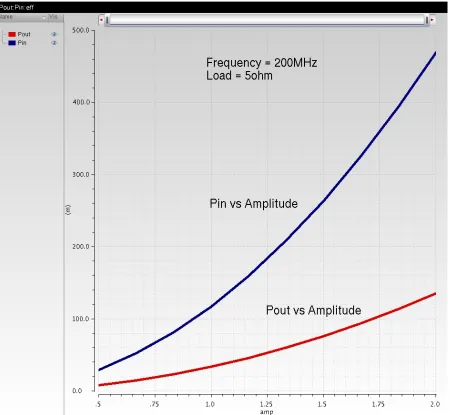
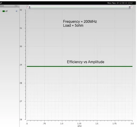
dependence on input amplitude. When input amplitude increases, the input and output power
both increase, while the power transfer efficiency keeps constant.
Figure 2.7 Power Transfer Efficiency as a function of input Amplitude
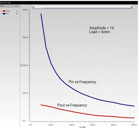
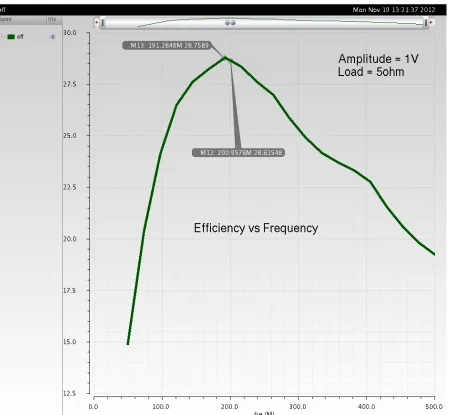
Figure 2.8 and 2.9 show input power, output power and power transfer efficiency’s
dependence on operation frequency. When input amplitude increases, the input and output
Chapter 3
System Design
3.1
System Overview
When considering inductive coupled interconnect (LCI) to transmit audio signal; the first
intuition is to send the amplified analog audio signal directly across it. In this case, the
transmitter side of headphone does not need any changes from the current TRS design.
However, this idea was abandoned due to the frequency character of the inductive coupled
channel. As shown in chapter 2, the LCI we use operates as a band pass filter, whose pass
band locates at MHz to GHz range. At frequency as low as audio, namely 20 Hz – 20 kHz,
attenuation dominates. Instead, LCI is capable of transmitting digital data and they will be
easily recovered at receiver side. As a result, the operations of analog to digital converting,
power amplifying, which are usually handled at transmitter side in conventional TRS
connector structures, have to be moved to the receiver side. Therefore, the processing of
audio data through LCI ends up consisting of three main steps:
1. Sending sampled digital audio data across LCI
2. Data recovery
3. Converting the digital audio into analog audio signal, power amplifying it to drive the 32
Ω load
component of a digital signal, a near field power scheme is used here: the larger LCI channel
transferring a high frequency sine wave, which will later be rectified into local DC voltage
supply.
The first version of block diagram of system is shown in fig 3.1
Figure 3.1 First version of system design (DAC and clock channel included)
A critical block in this proposed system is the power amplifier. Class D audio power
amplifier (PA) is used here. Compared with linear audio PA classes such as Class A, B and
AB, Class D PAs have higher power supply efficiency. In linear PAs, significant amounts of
power are lost due to biasing elements and the linear operation of the output transistors [5].
Because the transistors of a Class D amplifier are simply used as switches to steer current
through the load, minimal power is lost due to the output stage. The most basic topology
utilizes Pulse-Width Modulation (PWM) with triangle wave oscillator. Figure 3.2 shows a
Figure 3.2 Block Diagram of Conventional Class D Power Amplifier
The input analog audio signal is pulse-width modulated by the triangular signal,
generating a square wave, of which low-frequency portion of the spectrum is the wanted
output signal. Then the binary wave-form is amplified by witching the power devices, which
is a cascade of inverters whose final transistors have a large W/L ratio to obtain low output
impedance. Before driving the load, a passive low pass filter removes the unwanted
high-frequency components. The switching high-frequency is typically chosen to be ten or more times
the highest frequency of interest in the input signal.
Note that in order to use this type of Class D PA, the input audio data has been
converted several times between analog and digital forms, as shown in figure 3.3
signal directly from digital audio signal, which will also reduce the power budget and ease
the design effort for power supply circuits. The detailed method of generating PWM signal
from digital input will be discussed in chapter 4 circuit implementation. The second version
of block diagram of system is shown in fig 3.4
Figure 3.4 Second version of system design (clock channel included)
3.2
Synchronization and Alignment Scheme
Due to constrained number of pads on chip and the existing synchronization flaw
with previous version of design, the clock is recovered from data instead of transferred
through a separate channel. This brings up two important design considerations in systems
with transceiver, we now require a synchronization scheme and alignment scheme.
source synchronous, which sends a copy of the clock along with the data. It introduces
asynchronous issues when clock speed keeps increasing. The clock data recovery scheme,
which falls into the self synchronous model, is more robust against source synchronous
method. By adding the PLL-based clock recovery circuit, clock channel can be eliminated.
Alignment is another significant aspect in series link design. The deserializer at
receiver side is clocked by such an alignment signal to accurately recognize data boundaries
in the serial data stream. By adding an external reset signal and internal counter, and with the
help of local generated clock, alignment can be easily handled.
The finalized system design is shown in figure 3.5
Chapter 4
Circuit design
4.1
Pulse signaling in LCI --- Transceiver Design
A LCI transceiver, shown in figure 2.1, utilizes current mode pulse signaling [8]. Upon
the input NRZ data, a differential driver controls the directions of current swing in the
primary inductor, and creates an alternating magnetic field that induces current pulses in the
secondary inductor. A differential receiver senses the current pulses, converting them into
voltage pulses, then amplifies and latches into original NRZ data.
4.1.1 Transmitter
A current mode Transmitter is shown in figure 4.1
Tx_in_pos
Tx_in_neg
Vbias
Tx_out_pos
Tx_out_neg
R1
R2
M0
M1
M2
The transmitter should generate high edge rate to signal through the inductive coupled
channel, as well as providing accurate impedance match. A differential current mode
transmitter has the advantages of generating signal with true balanced rising/falling edges,
easier to impedance match. The downsides of current-mode driver compare to voltage-mode,
are less power efficient and slower slew rate.
The output impedance of this differential common source driver, Rout is Rout = R1 || ro
Where ro represents output resistance of input NMOS and R1 is termination resistance. By sizing M1, M2 and R1 accordingly, the output impedance is around 50 Ω which matches the characteristic impedance of the primary side coil. In actual implementation, multiple digitally
controlled current sources are added, which provides the ability to discretely control the
driving force accordingly.
Implementing in 0.13um CMOS technology with a 1.2 V power supply, the power
consumption of the differential current-mode driver is around 3 mW.
4.1.2 Receiver
The low swing complementary pulse receiver [8] includes three stages shown in figure
4.2: sensing, amplifying and converting. It senses current pulses on secondary coil,
converting them to voltage pulses, amplifying to rail-to-rail RZ signal, and converts back to
Q Q SET CLR S R Rx_in_pos Rx_in_neg Rx_out_pos Rx_out_neg Sense Amplify Convert M1 M2 M3 M4 R1 R2
Figure 4.2 Pulse Receiver
The input termination resistor matches the characteristic impedance of secondary coil
and converts the input current pulses into voltage pulses. A common gate single stage
amplifier is used in the sensing stage, due to its relatively low input impedance. Since the
input DC point at secondary coil is almost at ground, the common gate not only amplifies the
voltage pulses, but also leverages DC point onto a reasonable value for the next stage
pulse will be while lowering DC operating point at its output and more power consumption.
For the final implementation, a matched termination resistor is chosen. Another trade-off lies
between the DC operating point of output node and gain of first stage. By increasing the size
of diode connected PMOS load M1, a higher DC operating can be achieved while lowering
the small signal gain. In actual design, the sensing stage and amplify stage are co designed to
achieve a high gain with relatively wide bandwidth.
The Rx amplifying stage includes a pair of self-biasing, source coupled differential
amplifier [9] and a symmetric Chappell amplifier [10]. The tradeoff is between bandwidth
and gain. To amplify voltage pulses, a width bandwidth lower gain amplifier is preferred, to
minimize amplifier introduced distortion.
M1
M2
M3
M4
Vin+
Vin-Vout
M0
devices is chosen instead of NMOS. N-type current mirror is loaded to provide single-ended
output. The PFET current source is biased by the gate signal from the NMOS load. This
results in negative feedback that drives the bias voltage to the proper operating point [9]. If
the bias current is too low (high), the drain voltage rise (fall), increasing (decreasing) the bias
voltage. The quiescent power dissipation is around 240 uW.
The gain bandwidth plot is shown in figure 4.4
Figure 4.4 Frequency response of source coupled differential amplifier
M1 M2
Vin+
Vin-M5 M6
Vout- Vout+
M3
M4
M7
M8
Figure 4.5 Schematic of Chappell Amplifier
This circuit uses two current mirrors for the load, with each mirror driving one of two
current source devices. The negative feedback control of the bias current is the same as for
the single-ended Chappell amplifier. The signal at the differential output should be rail-to-rail
pulses to drive next sampling stage. The quiescent power dissipation is around 400 uW.
Figure 4.6 Frequency response of Chappell Amplifier
A RS latch is used to converting the RZ voltage pulses into NRZ digital signal, shown
in figure 4.7. Figure 4.8 shows the waveforms in each stage of transceiver when a 100 MHz
S
R
Q_bar
Q
RS Latch
Figure 4.7 Schematic of RS Latch
TX Output
RX Input Current
RX Input Voltage
First Stage Amp Input
Chappell Output First Stage Amp
Output
RS Latch Output
Figure 4.8 Signaling of Pulse Receiver
recovered clock at the speed of 1.41 MHz (44.1 kHz×32), and de-serialized by a Serial-In Parallel-Out block shown in figure 4.9
Figure 4.9 Serial-In Parallel-Out
A 32 bits shift register performs the function of SIPO. Conventional low speed
master-slave flip-flips are used in it. The series in clock is generated by clock data recovery
at 1.41MHz. And the parallel out clock is provided by the Alignment block.
As mentioned before, the alignment of SIPO is done at every time the system restarts.
By adding all 00…01 before real audio data and resetting the flag value, the flag will set to
high and keeps high whenever the first 1 comes. Flag is used as the reset signal of the
following divide-by-32 clock divider. As long as flag goes to high, clock divider will
generate the reload signal, which is a 44.1 kHz clock, used for SIPO output latching. The
D Q Clk Reset Q 1 0
Data
Reset
Flag
Clock DividerClock
Reload
Figure 4.10 (a) Schematic of Alignment
Clock
Reset
Data
Flag
Reload
Figure 4.10 (b) Timing Diagram of Alignment
4.3
Class D Power Amplifier
4.3.1 Introduction
Upon the two channel 16 bits audio signal received and de-serialized, they are power
Class D power amplifier is used here instead of linear audio power amplifier such as A,
B, and AB. In linear amplifiers, significant amounts of power are lost due to biasing elements
and the linear operation of the output transistors. Because the transistors of a Class D
amplifier are simply used as switches to steer current through the load, minimal power is lost
due to the output stage. The Class D PA can also be advantageous due to its ability to directly
interface to digital input signal, thereby eliminating the need for a digital-to-analog converter.
Class D amplifier work by generating a square wave of which the low-frequency portion of
the spectrum is essentially the wanted output signal, and of which the high frequency portion
serves no purpose other than make the wave-form binary so it can be amplified by switching
the power devices.
All Class D PA encode information about the audio signal into a stream of pulses.
Generally, the pulse widths are linked to the amplitude of the audio signal. The most
common Class D power amplifier comprises of Pulse-Width Modulation (PWM) process and
an output stage. Conceptually, PWM compares the input audio signal to a ramping waveform
Figure 4.11 Pulse Width Modulation [11]
There are basically two types of Class D PA corresponding to the form of input audio
signal. Analog Class D PA generates ramping signal with an oscillator and samples the
analog input audio signal by comparing it with the carrier, using a high resolution comparator.
This kind of implementation requires digital to analog converter if inputting digital audio
signal.
Digital Class D PA samples input audio data, and generates PWM signal by
algorithmic-based processes. The reported methodologies to generate the PWM pulse signals
in a digital PWM include uniform process [12], linear interpolation (LI) [12], pseudo-natural
PWM [13], static-filter PWM [14], weighted PWM and its variants [15], derivative PWM
Class D PA. The uniform process [12], which is used in this design, despite its high total
harmonic distortion (THD), offers a simpler design and less power consumption for this
demonstrative type of work. The triangular carrier in uniform sampling can be regarded as an
up/down digital counter, as shown in figure 4.12
Analog Digital Counter
Source
T
PWM
T
Figure 4.12 Single-sided trailing edge uniform sampling
Similar to conventional Class AB amplifiers, Class D PA can be categorized into two
topologies, half-bridge and full-bridge configurations [20], as shown in figure 4. 13.
Full-bridge provides better performance, 1) the Full-bridge topology can cancel the even order of
harmonic distortion components and DC offsets, 2) it allows the use of ternary modulation
M0 M1 PWM_A PWM_B M2 M3 M4 M5 PWM Full Bridge Half Bridge
Figure 4.13 Half Bridge and Full Bridge configurations of output stage in Class D Power Amplifier
PWM Generator PWM Generator Audio 44.1kHz, 16bits PWM_A PWM_B PWM Inverted Original
Figure 4.14 Block diagram of Ternary modulation
In ternary modulation, as shown in figure 4.14 and figure 4.15, original digital audio
signal and its complementary value are fed into two PWM generators, generating two binary
signals that, when subtracted, generated the three level value. In ternary modulation, there are
only current pulses flow through the load, while in conventional binary PWM, there is
Analog Audio
Original Sample
Carrier
Original
T
PWM
_
A
T
Inverted
T
PWM
_
B
T
Inverted Sample
T
4.3.2 Block Implementation of PWM
A hybrid PWM pulse generator [22] is implemented here, shown in figure 4.16. It
comprises faster clock method and tapped-delay-line method. In digital system, PWM signals
are typically created by using a faster clock method, and the counter clock frequency is
chosen to be 2N times the sampling frequency, where N is the number of bits of input data. In
this design, if implementing faster clock method, the counter clock speed = 44.1 kHz×216 = 2.89 GHz. It results in a tougher PLL design and more power consumption, which is not
acceptable in this design. One way to significantly reduce clock speed is to use a tapped
delay line [21]. The essential components of a tapped delay line PWM circuit are the delay
line and a multiplexer shown in figure 4.16. An M bits tapped delay line can reduce the clock
speed by 1/2M. In this design, hybrid of counter clock method and tapped delay line method are implemented. The 16 bits audio data is partitioned into 13 bits most significant portion
(MSP) and a 3 bits least significant portion (LSP), and they are the inputs to a down counter
and a tapped delay line. Thus, the counter clock speed reduced to 44.1 kHz×213 = 361 MHz.
Clock
Reload
PWM Zero_detect
Multiplexer
tp1
tp
Figure 4.17 Timing diagram of hybrid PWM generator
The timing diagram in figure 4.17 shows how it works. The reload clock and counting
clock are set at 44.1 kHz and 361 MHz, respectively. The PWM signal set to high on the
rising edge of Reload, when new 16 bits of input value are loaded in. then the down counter
will commence counting down the 13 bits MSP to zero. When the counter reaches zero, the 3
bits tapped delay line is initiated. The 3 bits tapped delay line is divided into eight equal
clock periods and selected by an 8 to 1 multiplexer whose output depends on the value of
LSP. The overall PWM pulse width is equivalent to the 16 bits digital value.
The total delay of the tapped delay line is adjusted so that the total delay is equal to
the counter clock period. By sizing the CMOS inverters appropriately, the propagation delay
can be adjusted. The ideal propagation delay of each stage should be T = 1/2.89 GHz = 346
4.4
Clock Recovery
4.4.1 Introduction
Due to constrained number of pads in this design, clock signals used in transmitter
side have to be recovered from data and generated using PLL. There are two clocks needed,
the 1.4112 MHz (44.1 kHz×25) sample clock fs for deserializer and 361 MHz (44.1 kHz× 213) counter clock f
c for PWM generator.
The sample clock can be recovered from the audio data while the sample clock will
be generated with an integer-N frequency synthesizer, which N =28. Combining these two structures together, a clock recovery circuit with an N divider is able to recover the sample
clock and generate the counter clock as well, as shown in figure 4.18
Figure 4.18 Block diagram of clock recovery
The proposed PLL based clock recovery circuit consists of a phase detector, a charge
and input data. The charge pump converts voltage into current, allowing the loop filter
suppresses high –frequency components in the PD output, generating a DC value to control
the VCO frequency. The VCO oscillates at a frequency, which divided by N, equal to the
input data speed and with a same phase difference as previous cycle.
4.4.2 Phase Detector
A conventional phase detector used in PLL is a circuit whose average output is
linearly proportional to the phase difference. However, in clock data recovery scenario, the
spectrum of random data exhibits a null at the bit rate [24], and the phase detector used for
periodic signals my completely fail if they sense random data. Thus the PD for random data
must provide two essential functions: 1) data transition detection and 2) phase difference
detection.
A phase detector can be classified as linear or binary type according to the clock
extraction method. The linear PD detects both the magnitude and the polarity of the phase
error whereas the binary PD detects the polarity only. Both of them produce a zero output for
non-transitions. Compared to binary PDs, linear PDs result in less charge pump activity,
smaller ripple on the oscillator control line, and hence lower jitter [25]. On the other hand,
the linear phase detector suffers from bandwidth limitation, which limits its usage in high
speed CDRs.
The binary PD generates up/down signals corresponding to the phase error between
(Bang-advantages of binary PDs (simplicity and accuracy) overcome the drawbacks of nonlinearity
and self-generated jitter.
In this design, Alexander PD is used and modified into a linearized version, shown in
Fig. The Alexander PD operates as follows: for any data transition, if the current sample
value agrees with previous falling edge sample is early, if the current sample value agrees
with next falling edge sample is late. The detailed timing diagrams for both late and early
cases are shown in figure 4.20.
Clock
Data
Early
Late
A
B
C
D
XNOR
Early_p
Late_p
XOR
Late Case
Clock
Data
Early
Late
A
B
C
D
XNOR
Early_p
Late_p
XOR
Early Case
Figure 4.20 (b) Timing diagram of sampling before mid point
The binary characteristic of Alexander PD also affects the steady-state behavior of
Clock Recovery Circuit [26]. The digitally feedback feature is not able to converge to a
single state due to the discontinuity of quantization process even if the difference of input
and output is close to zero. In steady-state, the system exhibits bounded periodic oscillations
Bang-bang PD, are AND with a linear term --- the mismatch between data and clock (named
XOR figures and timing diagram), to linearize the outputs.
4.4.3 Charge Pump & Loop Filter
The charge pump circuit comprises of two transconductance devices that are driven
with Early and Late outputs of phase detector, converting the digital phase error voltage into
charging or discharging current shown in figure 4.21 [27]. The choice of Gm is more related to the stability of the close loop. Note that charge-pump current (or Gm) provides gain for the close loop, it should be set relatively small to meet the stability requirement.
The combination of charge pump and C1 is an integrator that generates the average of
Early or Late pulses, which adjusts the oscillating frequency of VCO. Since there is another
integrator in VCO, the loop gain of this Type-II PLL has two poles at origin, thus, the closed
loop system is unstable. In order to stabilize the system, a zero is introduced in the loop gain
by adding a resistor R in serial with that capacitor.
To increase the out-of-band attenuation, an additional pole is created by adding a
secondary capacitor in parallel with the RC [28]. The pole, with a time constant of RC2,
filters high frequency ripples. The value of secondary capacitor is limited by stability and
filtering requirements.
In S domain,
FLF(s) =
1 C2
S
As shown in above expression, C1R defines the added zero and C2R defines the added second pole. The value of C2 should be set relatively small to minimize its effect on the close loop stability.
Late
Early
Ctrl
M1
M2
M3
M4
M5
M6
R
C1
C2
|T
(jw
)|
Angle
(T
(jw
))
-90
-180
PM
Figure 4.22 Phase Margin
4.4.4 VCO
An oscillator is an autonomous system that generates a periodic output without any
input. Generally there are two types of oscillators, LC tank oscillator and ring oscillator. LC
tank oscillators feature high accuracy and good phase noise, thus are widely used in wireless
systems design using any digital CMOS fabrication process. They are popular in CDR
circuits and on-chip clock distribution. A voltage controlled ring oscillator is shown in figure
4.23.
Clock
Vctrl
Bias_p
Bias_n
Figure 4.23 Schematic of Voltage Controlled Ring Oscillator
It comprises of two parts, a biasing generation and an inverter chain, as shown above.
Frequency tuning can be done in various ways: by tuning the load capacitance, by tuning the
driving strength, or by varying supply voltage. Figure 4.24 shows an implementation where
the strength of an inverter is changed by adding two more transistors, M1 and M5, to the
inverter structure, which is called single-ended current starve inverter. This type of stage
offers great simplicity and power efficiency while suffers from common mode problems.
More robust VCO such as differential ring oscillator can be used. Due to complexity and
power constrains, single-ended ring oscillator is used in this design.
modifying the single stage delay and number of stages, the frequency can be adjusted. Fewer
stages lead to less power consumption. Thus, one of the goals for this design is to reduce the
number of stages. The tuning range is the range of oscillating frequency the VCO can
achieve. It can be defined as a raw frequency or as normalized percentage. For this design,
there is no need for a large tuning range. In order to achieve a relatively narrow tuning range
of 10%, partially tuned current sources are introduced, shown in figure 4.24, in which M2
and M6 are always on. By adjusting the size of M1 and M5, tuning range can be changed.
VCO (KVCO) gain defines the change in output frequency divided by the change in control voltage. It can be regarded as the sensitivity of output frequency to the control voltage.
Bias_p
Bias_n
Vin
Vout
M1
M2
M3
M4
M5
M6
4.4.5 Results
Schematic simulation results of the PLL are shown in figure 4.25.
Clock
Data
Early
Late
Control
Figure 4.25 Schematic simulation result of clock recovery
4.5
Rectifier
All the circuits on the receiver side of this proposed headphone driver need to be
powered wirelessly. A high frequency sine wave is transmitted onto the primary coil, coupled
to secondary coil, and converted into DC power supply by a Rectifier, as shown in figure
~
~ +
-
Vdc = 1.2V
Figure 4.26 Powering scheme with LCI
An efficient power rectifier is required, which is able to provide stable 1.2 V power
supply with a 50 mA peak current. Rectifiers can be broadly categorized in two types, half
wave rectifiers and full wave rectifiers. The half wave rectifier is inefficient as it just uses
one half of each complete sine wave of the RF signal to convert it to a DC voltage. In the
other hand, full wave rectifier makes use of the entire input signal. Before analysis of several
different topologies of full wave rectifier, the most important performance metric of rectifiers,
Power Conversion Efficiency (PCE) should be mentioned here. PCE of rectifier is defined by
the output power POUT divided by the input power PIN. The input power can be written as the sum of output power and the loss of rectifier PLOSS. Therefore, PCE can be written as follows:
PCE = POUT PIN =
POUT
POUT+PLOSS =
POUT
POUT+N·PDIODE
Where N is the number of diode stages and PDIODE is the power loss of each diode [29]. A conventional full wave rectifier, which is composed of multi-stage of voltage multiplier, is
Figure 4.27 Multistage Voltage Multiplier
Let’s start the analysis with a single stage Voltage Multiplier, as shown in figure 4.28:
D1 D2
C1
C2
A
B
Clamping Peak Detector
Figure 4.28 Single stage conventional rectifier
This single stage rectifier comprises of two parts, clamping and peak detector. Diode
D1will be on whenever voltage at node below -VT, where VT is the turn on voltage of diode. This operation makes sure that voltage at node A is always higher than -VT. D2 and C2 form a peak detector, which detects the highest voltage from node A and keeps it at B. The overall
waveforms are shown in figure 4.29. The output voltage of a single stage rectifier at node B
is
Vrf Vt 2Vrf-Vt Vin Va Vb 2Vrf-2Vt T T
Figure 4.29 Waveforms of single stage rectifier
Note that the smaller the VT is, the larger the VDC becomes. For rectifiers with multiple stages, the output voltage will be
VDC = N (2VRF - 2VT)
where N is the number of stages.
As shown in [30], the PCE formula for conventional rectifier circuits can be
represented as:
PCE = VRF−VT VRF
Again, the smaller the VT, the larger the PCE becomes. It can be said that the small VT is essential in order to achieve large PCE of a rectifier.
In order to reduce the effective turn-on voltage for achieving larger PCE, several VT cancellation schemes have been proposed [30]-[33]. Fig 4.30 shows the unit stage of a
Vdc
Vrf+
Vrf-Vx
Vy
M1
M2
M3
M4
C3
C1
C2
Figure 4.30 Single stage differential CMOS rectifier
Two VT reduction schemes are used here. Voltage waveforms of internal nodes Vx and Vy obtained by simulation are shown in figure 4.31. NMOS transistor M1 and capacitor
C1 together clamps Vx higher than -VT, same as Vy. The DC components of Vx and Vy acts
as a kind of static gate bias voltage compensating VT, which is self-Vt-cancellation scheme [33]. In addition, in this differential structure, the gate of transistors is actively biased by a
Figure 4.31 Internal node voltage waveform
Different operating conditions have been analyzed to achieve a high PCE as well as
sufficient output voltage and current. The simulations are carried out with load resistance of
a. Amplitude of input sine wave
Increasing sine wave amplitude
Figure 4.32 Simulated amplitude dependence of output DC voltage
Figure 4.34 Simulated amplitude dependence of PCE
The amplitude of input sine wave is swept from 0.5 V to 1.5 V with 11 points. Figure
4.32 and 4.33 demonstrate that larger the input amplitude, higher the output DC voltage, as
well as the output DC current. This is consistent with the above shown analysis of rectifier
basics. Figure 4.34 shows PCE dependence on amplitude of input since wave. PCE increases
with higher amplitude. With a constant VT, larger the input amplitude, higher PCE achieved.
b. Frequency of input sine wave
Increasing sine wave frequency
Figure 4.35 Simulated frequency dependence of output DC voltage
Figure 4.37 Simulated frequency dependence of PCE
The frequency of input sine wave is swept from 50 MHz to 500 MHz with 7 points.
Figure 4.35 and 4.36 demonstrate that higher the frequency, higher the output DC voltage, as
well as the output DC current. Figure 4.37 shows PCE dependence on frequency of input
since wave. PCE peaks at around 200 MHz, which is the operating frequency of this design.
Input power almost linearly increases with frequency, while output power slows down. This
is because energy loss caused by the parasitic resistance increases with the increase in the
4.6
Results and Discussion
4.6.1 Layout
Out_Rp Vout_demo Rec_demo_inn Rec_demo_inp Rx_demo_inp Rx_demo_inn Rec_inp Rec_inn Clock Vbias Tx _ inp _ data Tx _ outn _ data Tx _ outp _ data Rx _ inn _ data Rx _ inp _ data Vdc
Lp Data Reload Ln
C_13 C_5 Rp Rn
Gnd Clock Sel Demo Rectifier Output Buffer & PWM Clock Recover 1mm 1mm
4.6.2 Simulation results
The entire design is simulated with a single tone 5 kHz audio, which is sampled at 44.1
kHz with resolution of 16 bits. A transient simulation result of voltage across 32 Ω load
resistor is shown in figure 3.39 (a). The corresponding frequency spectrum of the output
audio is calculated and plot in figure 3.39(b). It is clearly shown that the 5 kHz single tone is
recovered, while generating more content at the harmonics of the original frequencies.
(a) (b)
Table 4.1 summarizes the power dissipation of this design.
Table 4.1 Performance Matrix of Headphone driver with LCI
Technology IBM 0.13μm CMOS
Area 1mm by 1mm
Power Dissipation
TX 3mW
RX 1mW
Deserializer 200uW
Alignment 100uW
Clock Recovery 400uW
PWM Generator 400uW
Output Buffer (include load) 50mW
Chapter 5
Conclusion
5.1
Summary
In this thesis, several system design topologies of contactless headphone driver with
inductive coupled interconnection have been proposed. (Ch3) Their advantages and
disadvantages have been discussed. A self-synchronous, full digital and filterless topology is
implemented in IBM’s 0.13 μm 8RF process.
The differential CMOS rectifier previously used in RF harvesting field has been
demonstrated to provide peak power of 60 mW, which is enough to drive all the circuitry at
receiver side. (Ch4)
5.2
Future Work
The contactless headphone driver work can be extended in many directions.
5.2.1 Improvement of Disparity and Alignment Scheme
Clock recovery circuits require certain running disparity of transmitted data to reduce
clock drifting due to the lack of edges in data. Coding schemes can be introduced to ensure
running disparity, provide block alignment and error detection. The 8b10b encoding scheme,
5.2.2 Bi-directional Channel
a. Adaptive Powering
Due to the fast transition between different output currents in ternary PWM, the sine
wave used for ac powering has to be amplitude modulated off-chip. This can be
simplified by enabling feedback of PWM signal from receiver side to transmitter side. It
requires a bi-directional inductive coupled channel which allows feedback control.
b. Contactless headset driver
A contactless version of today’s widely used headset connector, TRRS, which
enables both listening and talking.
5.2.3 Audio Quality Control
For demonstration purpose, this work does not focus much on improving audio
quality. By introducing algorithmic-based PWM schemes, audio quality would be improved.
5.2.4 Data Modulation
By modulating data onto the sine wave, which is used for powering, will eliminate the
BIBLIOGRAPHY
[1] International Library of Technology: Principles of Telephony. Scranton, PA:
International Textbook Company, 1907.
[2] http://en.wikipedia.org/wiki/TRS_connector
[3] Rohrbach, Matthew Dean Doutt, Mark Edward Andre, Bartley K. Lim, Kanye DiFonzo,
John C. Gery, Jean-Marc, "Magnetic connector for electronic device," U.S. Patent 7
311 526, December 25, 2007
[4] Mick, S.; Wilson, J.; Franzon, P.; , "4 Gbps high-density AC coupled interconnection,"
Custom Integrated Circuits Conference, 2002. Proceedings of the IEEE 2002 , vol.,
no., pp. 133- 140, 2002
[5] Application Note 3977, Class D Amplifier: fundamentals of operation and recent
developments, Maxim Integrated Products, San Jose, CA, Jan 31, 2007
[6] http://en.wikipedia.org/wiki/Class-D_amplifier
[7] high speed serial I/O made simple, 1st ed., Xilinx inc., San Jose, CA, Apr 2005
[8] Jian Xu, "AC Coupled Interconnect for Inter-chip Communications," Ph.D. dissertation,
Dept. Elect. Eng., North Carolina State Univ., Raleigh, NC. 2006.
[9] W. J. Dally and J. W. Poulton, Digital Systems Engineering. New York: Cambridge
University Press, 1998
[10]Chappell, B.A.; Chappell, T.I.; Schuster, S.E.; Segmuller, H.M.; Allan, J.W.; Franch,
R.L.; Restle, P.J.; , "Fast CMOS ECL receivers with 100-mV worst-case sensitivity,"
[12]Mellor, P.H.; Leigh, S.P.; Cheetham, B.M.G.; , "Improved sampling process for a
digital, pulse-width modulated, class D power amplifier," Digital Audio Signal
Processing, IEE Colloquium on , vol., no., pp.3/1-3/5, 22 May 1991
[13]Mellor, P.H.; Leigh, S.P.; Cheetham, B.M.G.; , "Reduction of spectral distortion in
class D amplifiers by an enhanced pulse width modulation sampling process," Circuits,
Devices and Systems, IEE Proceedings G , vol.138, no.4, pp.441-448, Aug 1991
[14]Goldberg, J.M.; Sandler, M.B.; , "New high accuracy pulse width modulation based
digital-to-analogue convertor/power amplifier," Circuits, Devices and Systems, IEE
Proceedings - , vol.141, no.4, pp.315-324, Aug 1994
[15]L. Risbo and T. Morch, “Performance of an all-digital power amplification system,” in
Proc. 104th AES Convention, May 1998. Preprint no. 4695.
[16]M. Johansen and K. Nielsen, “A review and comparison of digital PWM methods for
digital pulse modulation amplifier (PMA) systems,” in Proc. 107th AES Convention,
Sep. 1999. preprint no.5039.
[17]Z. Song, “Digital pulse width modulation: analysis, algorithms, and applications,” Ph.D.
dissertation, Univ. Illinois at Urbana-Champaign, Urbana, 2001
[18]C. Pascual and B. Roeckner, “Computationally efficient conversion from pulse-code
modulation to naturally sampled pulse-width modulation,” in Proc. 109th AES
convention, Sep. 2000. Preprint 5198.
[20]Application Note AN-1071, Class D Audio Amplifier Basics, International Rectifier
Corp., EI Segundo, CA
[21]Bah-Hwee Gwee; Chang, J.S.; Huiyun Li; , "A micropower low-distortion digital
pulsewidth modulator for a digital class D amplifier," Circuits and Systems II: Analog
and Digital Signal Processing, IEEE Transactions on , vol.49, no.4, pp.245-256, Apr
2002
[22]Dancy, A.P.; Chandrakasan, A.P.; , "Ultra low power control circuits for PWM
converters," Power Electronics Specialists Conference, 1997. PESC '97 Record., 28th
Annual IEEE , vol.1, no., pp.21-27 vol.1, 22-27 Jun 1997
[23]Behzad Razavi, "Design of Monolithic Phase-Locked Loops and Clock Recovery
Circuits --- A Tutorial," Dept. Elect. Eng., UCLA, Los Angeles, CA
[24]Behzad Razavi, "Clock and Data Recovery," in Design of Integrated Circuits for
Optical Communications, New York: McGraw-Hill, 2003, ch. 9, pp. 288-332.
[25]Savoj, J.; Razavi, B.; , "A 10-Gb/s CMOS clock and data recovery circuit with a
half-rate linear phase detector," Solid-State Circuits, IEEE Journal of , vol.36, no.5,
pp.761-768, May 2001
[26]Hyung-Joon Jeon, "A 10Gb/s Full On-chip Bang-bang clock and data recovery system
using an adaptive loop bandwidth strategy," M.S. thesis, Dept. Elect. Eng., TAMU.,
College Station, TX, 2009.
[27]Mozhgan Mansuri, "Low-Power Low-Jitter On-Chip Clock Generation," Ph.D.
[29]Ashry, A.; Sharaf, K.; Ibrahim, M.; , "A Simple and Accurate Model for RFID
Rectifier," Systems Journal, IEEE , vol.2, no.4, pp.520-524, Dec. 2008
[30]Koji, K.; Takashi, I.; , "Self-Vth-Cancellation High-Efficiency CMOS Rectifier Circuit
for UHF RFIDs," IEICE TRANS, ELECTRON, vol. E92-C, no. 1, Jan. 2009
[31]Umeda, T.; Yoshida, H.; Sekine, S.; Fujita, Y.; Suzuki, T.; Otaka, S.; , "A 950-MHz
rectifier circuit for sensor network tags with 10-m distance," Solid-State Circuits, IEEE
Journal of , vol.41, no.1, pp. 35- 41, Jan. 2006
[32]Nakamoto, H.; Yamazaki, D.; Yamamoto, T.; Kurata, H.; Yamada, S.; Mukaida, K.;
Ninomiya, T.; Ohkawa, T.; Masui, S.; Gotoh, K.; , "A Passive UHF RF Identification
CMOS Tag IC Using Ferroelectric RAM in 0.35-μm Technology," Solid-State Circuits,
IEEE Journal of , vol.42, no.1, pp.101-110, Jan. 2007
[33]Kotani, K.; Ito, T.; , "High efficiency CMOS rectifier circuit with self-Vth-cancellation
and power regulation functions for UHF RFIDs," Solid-State Circuits Conference,
2007. ASSCC '07. IEEE Asian , vol., no., pp.119-122, 12-14 Nov. 2007
[34]Kotani, K.; Sasaki, A.; Ito, T.; , "High-Efficiency Differential-Drive CMOS Rectifier
for UHF RFIDs," Solid-State Circuits, IEEE Journal of , vol.44, no.11, pp.3011-3018,

![Figure 4.11 Pulse Width Modulation [11]](https://thumb-us.123doks.com/thumbv2/123dok_us/1488052.1182061/39.612.184.442.67.291/figure-pulse-width-modulation.webp)
