Current Driver Circuit for Cancer Detection
and EIT Application
Pramod Kumar Jain,D. S. Ajnar,
Antima Mishra
Associate Professor (Micro Elex. & VLSI Design), Department of E & I, Shri G.S. Institute of Technology and
Science, Indore, India
Associate Professor (Micro Elex. & VLSI Design), Department of E & I, Shri G.S. Institute of Technology and
Science, Indore, India
P.G. Scholar (Micro Elex. & VLSI Design), Department of E & I, Shri G.S. Institute of Technology and Science,
Indore, India
ABSTRACT: Tissue exhibits property of both transconductor and dielectric. This property can be represented by its electrical impedance. A cancerous tissue has more impedance as compared to healthy tissue. The technique used to characterize the electrical impedance is Electrical Impedance Tomography. To measure the impedance is to inject a constant current through two electrode and measure the related voltage difference across the other pair of electrode. This paper is an attempt to provide a current driver circuit that uses negative feedback to provide a distortion less high output impedance circuit with optimum current. It is fabricated in a 0.18-μm complementary metal–oxide– semiconductor (CMOS) process technology, and operates from ±1.6V power supply. For a maximum output current of 0.5 mAp-p , the measured total harmonic distortion is below 0.5 %.The variability of current with respect to load is 1% which is.very less up to 1M Hz frequency then approximately
KEYWORDS: Electrode, Cancer Detection, Bio Impedance, DDTA (Differential Difference Transconductance Amplifier), Voltage Buffer
I. INTRODUCTION
The Electrical impedance measurement technique consists of characterisation of a biological material in terms of electrical impedance measured over a wide frequency range. Tissues have conductivity less than 10-7 S/m & have capacitance of typically 10-2 F/m2.The electrical impedance of biological tissue decreases with increasing frequency. The process of measurement involves application of current to tissue through one pair of electrodes and measuring the voltage through another pair of electrodes or through array of electrodes at different locations. The method is relatively less sensitive to changes in the electrode/tissue impedance of both voltage-sensing and current-injecting electrodes. The ac current driver must have sufficient accuracy over the total operational bandwidth, and its output must be independent of load variations ideally. The insensitive conditions of the tetra polar measurement are satisfied when the output impedance of the current generator circuit and the input impedance of the differential amplifier are large as compared to the sum of the electrode and tissue impedances. Variety of current drivers has been used previously, by using discrete designs such as the Howland circuit. In applications requiring high precision delivery of alternating current to biological loads, the output impedance of the Howland is a critical figure of merit that limits the precision of the delivered current when the load changes. Improvement in the Howland circuit done for the better result, but the drawback with Howland is that it cannot land itself to fully integrated circuit due accurate value of resister. Thus a fully integrated circuit is needed for cancer detection in tissue and for EIT application which can work over wide frequency with less distortion and optimum current
II. R
In [1] authors discussed about the use of Howland Circuit as current source which is used for many purposes where current sources or current drivers are needed but for integrated circuit it is not possible to place the matched value of registers that are needed. In this two parallel Howland opamp circuit were used. In [2] author used many transconductance and preamplifiers based on CMOS circuit and compared it with the Modified Howland circuit. In [3] a current driver circuit is being formed for respiratory tissue detection, it have supply voltage of maximum 18 volt. In [4] a DDTA circuit is explained which can be used instead a cascode amplifier used in [3] for better result. In [5] a FPGA based Modified Howland current pump circuit is formed but having less output impedance.
III.PROPOSED WORK
Current Driving Circuit:
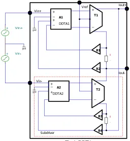
Fig. 1 shows the block diagram of the current driver. It consist of two identical single-input differential-output current drivers called subdrivers , i.e., one for sinking current and the other for sourcing current to generate a balanced voltage across the load. This design cancels the common-mode voltage error across the load due to a voltage imbalance, caused by sense resistor R1 (or R2), if a single current driver were to be used on its own (subdriver shown in Fig. 1). Each subdriver consists of a preamplification stage realized by a differential difference transconductance amplifier (DDTA1 “A1” or DDTA2 “A2” ), followed by a transconductor (T1 or T2 ), which performs the voltage-to-current conversion operation and drives the load. Sense resistor (R1 or R2 ) is used to monitor the output current of both the subdriver.the voltage across the register is feedback . The low-frequency transfer function (i.e., transconductance) of each subdriver when the load is assumed to be a resistor RL is given by
A. Description of the Proposed Circuit: DDTA
The DDTA work as an amplifier to improve overall transconductance of the circuit. The transconductance basically works as an preamplifier. The input to the circuit is applied by the circuitry including M5 and M6,.Two source degenrators are used as M6 and M8. The source degenerator works for linearity of the circuit. We make the transconductance of this circuit in such a value that it work as degeneration register gm=1/R. The degeneration technique eliminates the electronic tuning capability because its value is characterized by degeneration register .Due to this the circuit have better band width and noise performance. Current mirror M1, M2 & M3, M4 with M14,M15 form output for differential amplifier .The transistor M16 & M17 are working as common mode feedback control .
Fig.2. DDTA
B .Transconductor:
This transconductance work on three current mirror circuit which reduce its overall driving voltage. Common mode
M5A M5B
M2
M
6
B
M
6
A
M7A M7B
M
8
B
M3 M4
M10
M9 M11 M12 M13
M14
M16
M15
M17
M
8
A
M1
ib1 10u
Vss Vo1+
Vo1-Vo2+
Vo2-Vdd
output level but these entire transistor need to be in triode. Accuracy of the circuit get affected as these transistor moves from triode region.
Where Vg is the gate voltage, VT is the threshold voltage , Vov = 2Id /β is the overdrive (saturation) voltage, β is the process transconductance, Id is the drain current, Vo2_q is the quiescent point of outputs Vo2+ and Vo2− , VSS is the
negative supply voltage, and the subscript numbers in Vg , Vov , and β refer to the respective transistors
Fig.3.Transconductance
C..Voltage Buffer
The purpose of voltage buffer is to monitor the injected current to the electrode tissue load by floating voltage across sense register .The measured voltage is fed back to DDTA creating a negative feedback loop. Voltage buffer is differential to single ended design which is done with the help of transistor by current mirror differential to single ended. Transistor M1 to M4 form input stage. A capacitor is applied to maintain phase margin for the unity gain operation.
V
d
d
V
s
s
V
s
s
V
d
d
M3 M4
M5
M6 M7 M8
M1 M2
M10 M9
M12 M14
M11 M13
M15A
M16A
M15B
M16B Ibias2 45u
VI2+
VI2-IO+
IO-Vref
Fig.5. Voltage Buffer
IV.SIMULATION RESULTS
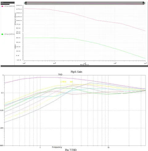
The current driver works on .18 μm technology, over all circuit works on ±1.6-V power supply. The simulation studies involve the determination of the output noise. The circuit stability with harmonic distortion determined by finding THD (Thermal Harmonic Distortion). The overall gain of differential amplifier and transconductance amplifier’s generated though the circuit. The overall power consumed through the circuit is 2W. The maximum output current is 0.5 μA.
Parameter 8th 9th 10th This Work
Bandwidth 90KHz 100-100KHz 1MHz 10K-1MHz
Output Current 350µ 400µ 500µ 0.5m
Power supply ±0.8V ±0.9V ±2.5V ±1.6V
M17
T2 2N6755 M16
M15
M1
M6 M7
M4
M8 M5
M10 M9
M12
M11 M13 M14
M18
Ibias3 50u
C1 1u
M2 M3
Vdd
Vss
Fig.6. Gain
Fig.8. Output Current
Fig.9. Output Noise
V. CONCLUSION AND FUTURE WORK
R
1. A. S. Tucker, R. M. Fox, and R. J. Sadleir, “Biocompatible, high precision, wideband, improved Howland current source with lead-lag
compensation,” IEEE Trans. Biomed, Circuits Syst., vol. 7, no. 1, pp. 63–70,Feb. 2013.
2. H. Hong, M. Rahal, A. Demosthenous, and R. H. Bayford, “Comparison of a new integrated current source with the modified Howland circuit
for EIT applications,” Physiol. Meas., vol. 30, no. 10, pp. 999–1007,Oct. 2009.
3. Constantinou, I. F. Triantis, R. Bayford, and A. Demosthenous, “High-power CMOS current driver with accurate transconductance for
electrical impedance tomography,” IEEE Trans. Biomed. Circuits Syst., vol. 8,no. 4, pp. 575–583, Aug. 2014
4. E. Sackinger and W. Guggenbuhl, “A versatile building block: The CMOS differential difference amplifier,” IEEE J. Solid-State Circuits,
vol. 22, pp. 287–294, 1987.
5. J.W. Lee, T. I. Oh, S. M. Paek, J. S. Lee, and E. J. Woo, “Precision constant current source for electrical impedance tomography,” in Proc.
25th Annu. Int. Conf. IEEE Engineering in Medicine and Biology Soc., Cancun, Mexico, 2003, pp. 1066–1069.
6. L. Constantinou, A. Demosthenous, P. Langlois, R. Bayford, and I.Triantis, “An improved CMOS current driver for electrical impedance
tomography,” in Proc. 20th Eur. Conf. Circuit Theory and Design,Linköping, Sweden, 2011, pp. 290–293
7. L. Yan et al., “A 3.9 mW 25-electrode reconfigured sensor for wearable cardiac monitoring system,” IEEE J. Solid State Circuits, vol. 46, no.
1, pp. 353–364, Jan. 2011.
8. S. Hoo et al., “A 4.9 mΩ-sensitivity mobile electrical impedance tomography IC for early breast-cancer detection system,” in Proc. IEEE ISSCC Dig. Tech. Papers, San Francisco, CA, USA, 2014, pp. 316–317.
9. Antima Mishra and P.K. Jain “:Low Power Wide Band Current Driver circuit for impedance measurement in Cancer Detection ”in
Proceedings of The National Conference on Advance Communication Technology organized by Ujjain Engineering College ,Ujjain (M.P.),December 1-2,2015,page no. 211-216.
10. A. S. Tucker, R. M. Fox, and R. J. Sadleir, “Biocompatible, high precision,wideband, improved Howland current source with lead-lag
compensation,”IEEE Trans. Biomed. Circuits Syst., vol. 7, no. 1, pp. 63–70,2013.
11. P. Bertemes-Filho, B. H. Brown, and A. J. Wilson, “A comparison of modified Howland circuits as current generators with current mirrortype
circuits,” Physiol. Meas., vol. 21, pp. 1–6, 2000.
12. H. Hong, M. Rahal, A. Demosthenous, and R. H. Bayford, “Comparison of a new integrated current source with the modified Howland circuit
for EIT applications,” Physiol. Meas., vol. 30, no. 10, pp. 999–1007, Oct. 2009.P. O. Gaggero, A. Adler, J. Brunner, and P. Seitz, “Electrical impedance tomography system based on active electrodes,” Physiol.
Meas., vol. 33, pp. 831–847, 2012.