ABSTRACT
KUMAR, MISHA. Control Implementations for High Bandwidth Shunt Active Filter. (Under the direction of Dr Subhashish Bhattacharya).
The presence of multiple harmonics in the power line due to various nonlinear consumer loads like adjustable speed drives, computers, etc incites the need for a high frequency active filter inverter so as to reduce the harmonic content at the point of common coupling (PCC) to be typically lower than 5% (for SCR<20) and 12%(for SCR=50-100) as specified by IEEE 519 harmonic standards. The objective of this thesis is to implement and compare three different active filter control techniques. These control techniques are based on Load Current, Supply Current and Vf (Voltage at Point of
Common Coupling) harmonic extraction methods. Based on the analysis done in this work, it has been found that the Vf harmonic extraction method provides better compensation (THD=3.34%) as
compared to the Load current (THD=3.82%) and Supply Current (THD=6.24%) harmonic extraction methods. A hardware board for harmonic extraction has also been built in the lab and its operation has been verified using three different types of nonlinear loads.
To provide the compensation for multiple harmonics in the power line, there is a need for the current controller which provides multiple frequency current tracking. Therefore, in this work, a Predictive current controller has been implemented on an analog board as a part of active filter control for providing current regulation. In the predictive current regulator, dead time compensation (3µsec) has also been performed in order to remove the effect of sampling and inverter dead time delay on PWM pulses and hence on the inverter output.
Control Implementations for High Bandwidth Shunt Active Filter
by
Misha Kumar
A thesis submitted to the Graduate Faculty of
North Carolina State University
in partial fulfillment of the
requirements for the degree of
Master of Science
Electrical Engineering
Raleigh, North Carolina
2011
APPROVED BY:
_______________________________ ______________________________
Dr. Mesut E. Baran
Dr. Srdjan M. Lukic
________________________________
Dr. Subhashish Bhattacharya
ii
DEDICATION
iii
BIOGRAPHY
iv
ACKNOWLEDGMENTS
This thesis has been successful due to the support of FREEDM system center, North Carolina State University.
I would like to express my gratitude to my advisor, Dr Subhashish Bhattacharya whose valuable guidance and support has helped me to steer through all the challenges I faced during my research. I would like to thank my committee members Dr Mesut E Baran and Dr Srdjan Lukic for giving me excellent understanding of courses like Power Systems, Renewable Energy Systems and Electric Motor Drives.
I would like to thank my friends and fellow colleagues Arvind Govindaraj, Siddharth Ballal, Urvir Singh, Arun Kadavelugu, Vijay Shanmugasundaram, Kamalesh Hatua, Awneesh Tripathi, Ankan De, Mihir Shah, Shailesh Notani, Priyadarshini Asokan, Eric Green, Ankita Upreti, Moyeen Ul Haq, Hesam Mirzaee, Babak Parkhideh, Edward Van Brunt, Ryan Meitl, Aaron Curry, Shaunta D. Mason, Danny Fregosi and Deepshikha Gangal. This thesis would not have been possible without the countless number of discussions and knowledge sharing sessions with them.
I would like to thank my parents, my brother and sister in law for their love, support and encouragement throughout my career.
Last but not least, this thesis would not have been possible by the constant emotional and mental support from my best friend Karan Kapoor. Thank you for your love and a very understanding nature.
v
TABLE OF CONTENTS
LIST OF TABLES ... viii
LIST OF FIGURES ... ix
CHAPTER 1. INTRODUCTION ... 1
1.1 Background ... 1
1.1.a IEEE 519 Harmonic Standards... 1
1.1.b Control of Harmonics and their Impacts ... 2
1.2 Thesis Objective ... 5
1.3 Outline ... 5
1.4 Glossary of Terms ... 6
CHAPTER 2. ACTIVE FILTERS ... 7
2.1 Review of Active Filter Topologies ... 7
2.1.a Shunt Active Filter ... 7
2.1.b Series Active Filter ... 8
2.1.c Hybrid Parallel Active Filter ... 10
CHAPTER 3.SHUNT ACTIVE FILTER CONTROLLER ... 12
3.1 Harmonic Extraction ... 12
3.1.a Synchronous Reference Frame Harmonic Extraction ... 12
3.2 DC Bus Voltage Control ... 19
3.3 Current Controller ... 20
3.3.a Predictive Current Controller with charge error control ... 20
3.3.b Space Vector PWM and its implementation in Analog Domain ... 23
3.3.c Implementation issues and Dead Time Compensation ... 25
vi
3.5 Active Filter System Specifications ... 26
3.6 Simulink/MATLAB Model and Simulation Results ... 27
3.6.a Simulation Results of System without Active Filter ... 27
3.6.b Active Filter Compensation using Supply Current Harmonic Extraction Method .... 29
3.6.c Active Filter Compensation using Load Current Harmonic Extraction method ... 32
3.6.d Active Filter Compensation using Vf (Voltage at PCC) Harmonic Extraction method ... 34
3.7 Comparison between the three different harmonic extraction methods ... 37
3.8 Summary ... 39
CHAPTER 4. FPAA AND FPGA IMPLEMENTATION OF SRF CONTROLLER ... 40
4.1 Field Programmable Analog Arrays ... 40
4.2 Simulation Results of Positive Sequence SRF Controller Using Simulink/MATLAB ... 42
4.3 Implementation of SRF Controller on FPAA ... 43
4.4 Implementation of SRF Controller on FPGA ... 46
4.5 Comparison of Analog FPAA and Digital FPGA Controller Outputs ... 47
CHAPTER 5.HARDWARE IMPLEMENTATION OF SHUNT ACTIVE FILTER SYSTEM ... 49
5.1 Nonlinear Load Specifications ... 49
5.1.a Diode Rectifier with DC side Inductor, and DC side Capacitor system ... 50
5.1.b AC Supply Side Line Inductor and Diode Rectifier with DC side Capacitor system 51 5.1.c AC Supply Side Line Inductor, Diode Rectifier with DC side Inductor, and DC side Capacitor system ... 53
5.2 Harmonic Extraction on an Analog Board ... 55
5.2.a Implementation delay of Analog harmonic extractor ... 56
vii
5.2.b.ii Vf (Voltage at PCC) Harmonic Extraction Results ... 60
5.2.b.iii Supply Current Harmonic Extraction Method Results ... 62
5.3 Predictive Current Controller Implementation on Analog Board ... 63
5.4 Active Filter Inverter System ... 66
5.4 Summary ... 69
CHAPTER 6.CONCLUSION ... 71
viii
LIST OF TABLES
ix
LIST OF FIGURES
Figure 1.A Passive Filter System ... 3
Figure 2.A Shunt Active Filter System ... 7
Figure 3. Series Active Filter System[10] ... 9
Figure 4.Hybrid Parallel Active Filter System ... 11
Figure 5.Block Diagram representation of Supply Current, Load Current and Vf harmonic extraction method ... 14
Figure 6.Harmonic Equivalent Circuit of Active Filter ... 15
Figure 7.Lead plus Proportional Characteristic of Active Filter Controller (Reproduced from [9]) .... 16
Figure 8.Predictive Current Controller with charge error control (Reproduced from [14]) ... 22
Figure 9. Block diagram of the Analog Implementation of the Space Vector PWM Technique ... 25
Figure 10.Parallel Passive Filter system used in Simulation ... 27
Figure 11.PLECS Model of a system having Non-Linear Load ... 27
Figure 12.Supply Current waveform for the system without active filter ... 28
Figure 13.FFT Analysis of the Supply Current Waveform for the system without Active Filter ... 28
Figure14. Vfa(l-n Voltage at PCC) of the system without active filter ... 29
Figure 15.Simulink Model of an Active Filter Controller using Supply Current Harmonic Extraction method ... 29
Figure 16.Supply Current waveform after the active filter compensation using supply current harmonic extraction method ... 30
Figure 17.FFT Analysis of Supply Current Waveform after compensation ... 30
Figure 18.Compensation current matching with the Load Current Extracted Harmonics ... 31
x
Figure 20.Simulink Model of the Active Filter Controller using Load Current Harmonic Extraction
Method... 32
Figure 21.PLECS Model of the System with Active Filter ... 32
Figure 22.Supply Current Waveform after the active filter compensation using load current harmonic extraction method ... 33
Figure 23.FFT Analysis of Supply Current Waveform after compensation ... 33
Figure 24.DC Bus Voltage Controlled at 680V ... 34
Figure 25. Simulink Model of the system with active filter controller using Vf harmonic extraction method ... 34
Figure 26.Supply Current Waveform after compensation using Vf harmonic extraction method ... 35
Figure 27.FFT Analysis of Supply current waveform after harmonic compensation using Vf harmonic extraction method ... 35
Figure 28. Compensating current, the harmonic current extracted from load current and Vfa ... 37
Figure 29. DC Bus Voltage Controlled at 750 V ... 37
Figure 30. FPAA Configuration Diagram [16], [17] ... 41
Figure 31. Anadigm’s AN231E04 FPAA Evaluation Board ... 42
Figure 32. ILa,ILb,ILc waveform input to the SRF Controller ... 42
Figure 33. e Lq e Ld
I
I
,
waveform obtained after the Park Transformation ... 42Fig34. e Ld e Lq
vs
I
I
... 43 Figure 35. s hq s hdI
I
,
waveforms ... 43Figure 36. Ihd and ILa waveform ... 43
xi
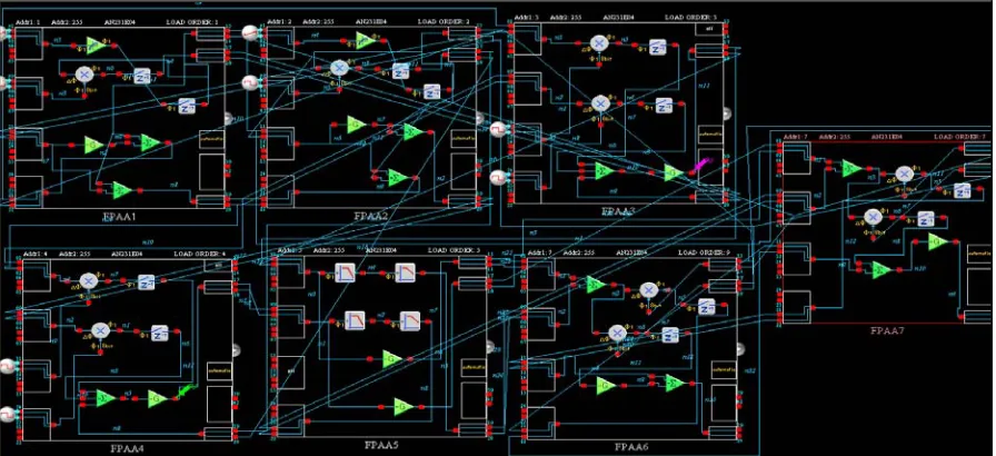
Figure 38. Laboratory Setup of seven FPAA boards to implement Positive Sequence SRF Controller
algorithm ... 44
Figure 39.Oscilloscope output showing waveforms for
I
Lde(
bottom
),
I
Lqe(
top
)
... 45Figure 40.Oscilloscope output showing waveforms for
I
hqs(
top
),
I
hds(
bottom
)
... 45Figure 41.Delay in Implementation on FPAA(17.4µsec)... 45
Figure 42.Plot of e Lq
I
vs e Ld I ... 45Figure 43. Positive Sequence SRF Controller Implementation on NI C-RIO(FPGA) using LABVIEW software ... 46
Figure 44.Oscilloscope output showing waveforms for Iha,Ihb,Ihc ... 47
Figure 45.Delay in Implementation on C-RIO(30µsec) ... 47
Figure 46.Hardware Setup of Shunt Active Filter Controller and the Nonlinear Load ... 49
Figure 47. Diode Rectifier with DC side Inductor, and DC side Capacitor system ... 50
Figure 48. Oscilloscope waveform for Scaled Isa,Isb,Isc ... 51
Figure 49. Oscilloscope Waveform for Scaled Three phase voltage Vfa,Vfb,Vfc ... 51
Figure 50. Diode Rectifier with AC supply side Inductor and DC side Capacitor system ... 52
Figure 51. Oscilloscope waveform for Scaled Isa,Isb,Isc ... 52
Figure 52. Oscilloscope Waveform for Scaled Three phase voltage Vfa,Vfb,Vfc ... 52
Figure 53. AC Supply Side Line Inductor, Diode Rectifier with DC side Inductor, and DC side Capacitor system. ... 53
Figure 54.Oscilloscope waveform for Scaled Isa,Isb,Isc ... 54
Figure 55.Oscilloscope Waveform for Scaled Three phase voltage Vfa,Vfb,Vfc ... 54
xii
Figure 57.Magnitude Bode Plot of the 5th order Butterworth Filter (Gain Normalized to the Cut off Frequency)(Reproduced from MAX280 Datasheet) ... 56 Figure 58.Oscilloscope waveform for ILa(yellow),Ihds(blue) ... 57
Figure 59.Zoomed Oscilloscope waveform for ILa (yellow),Ihds(blue) showing a delay of 4.8µsec ... 57
Figure 60.Oscilloscope waveform for iLa(blue),i (pink),iqe(green) e
d for load type explained in section 5.1.c ... 57 Figure 61. Oscilloscope waveform for iLa (blue), inverted low pass filtered
i
de(pink), inverted low pass filtered eq
i (green) ... 57
Figure 62.Oscilloscope waveform of s hd
i
(pink), s hqi (green) for load type explained in section 5.1.c .. 58
Figure 63. s hd
i
(pink),ifa(green),ifa-i
hds (yellow) ... 58 Figure 64.Oscilloscope waveform for iLa (green),i
de(blue),e q
i (pink)for load type explained in section 5.1.b ... 59 Figure 65.Oscilloscope waveform for iLa (green), inverted low pass filtered
i
de(blue), inverted low pass filtered eq
i (pink) ... 59
Figure 66. Oscilloscope waveform of s hd
i
(blue), s hqi (pink) for load type explained in section 5.1.b ... 59
Figure 67. Oscilloscope waveform for iLa (green),
i
de(blue), e qi (pink)for load type explained in section 5.1.a ... 60
Figure 68. Oscilloscope waveform for iLa (green), inverted low pass filtered
i
de(blue), inverted low pass filtered eq
i (pink) ... 60
Figure 69. Oscilloscope waveform of s hd
i
(blue), s hqxiii
Figure 70.Oscilloscope waveform for Vfa(pink),V
de(green),e q
V (blue) ... 60
Figure 71. Oscilloscope waveform for Vfa (pink), inverted and filtered
V
de(blue), e q V (green) ... 61Figure 72. Oscilloscope waveform for Vfa (blue),
V
ds(pink), s q V (green) ... 61Figure 73. Oscilloscope waveform for Vfa (blue),
i
hds (green), s hq i (pink)(for Kv=10) ... 61Figure 74. Oscilloscope waveform for isa (pink),i (green),isqe(blue) e sd ... 62
Figure 75. Oscilloscope waveform for isa (pink), inverted low pass filtered
i
sde (green), inverted low pass filtered e sq i (blue) ... 62Figure 76.Oscilloscope waveform for isa (pink) ,
i
sde (green) after gains
KT
s
KT
s
G
)
(
1
)
(
)
(
, e sq i (blue) after gains
KT
s
KT
s
G
)
(
1
)
(
)
(
,K=5,T=10-3 ... 62Figure 77.Oscilloscope waveform for isa(pink),
i
hds (green), s hq i (blue) ... 62Figure 78.
SV
invds* (blue), SVinvqs* (green)(Active Filter inverter reference voltages for SVPWM) ... 64Figure 79.
V
invan* ,V
invbn* ,V
invcn* (Three phase active filter inverter reference voltage for SVPWM) ... 64Figure 80.Triplen extraction for the SVPWM technique ... 64
Figure 81.Vamod,Vbmod ,Vcmod (Three phase modulating voltages for comparing with triangular waveform) ... 64
Figure 82.Sample and Hold(S/H) Pulses; S/H at Tsw(blue),S/H at Tsw/2(green) ... 65
Figure 83.Vamod after sample and hold operation ... 65
xiv
Figure 85.Inverter pulses for switches S1(blue),S3(pink) and S5(green) ... 65
Figure 86.Inverter pulses S1,S3,S5 enclosed in one another in 0127-7210 order and showing the SVPWM operation ... 65
Figure 87.Inverter dead band given to S1 and S2 pulses ... 66
Figure 88. Schematic of the active filter inverter system implemented in lab. ... 67
Figure 89. The experimental setup of the active filter inverter system ... 67
Figure 90.Inverter terminal voltages; Vinvan , Vinvbn at DC bus Voltage = 200V ... 68
Figure 91.DC bus Voltage(at 250V)(brown),Voltage across load(l-l)(blue),Ifa(pink) ... 68
1
CHAPTER 1. INTRODUCTION
1.1 Background
With the advancement in Power Electronic technology, these days various consumer and industrial loads in the power system are nonlinear loads such as Adjustable Speed Drives with diode rectifier front end, Computers, Fax Machines, PLC’s, High Power diode Rectifiers, Cycloconverters etc. These Nonlinear loads draw nonsinusoidal currents from utilities due to their operation thereby causing a poor power quality at the utility side. The harmonics are generated when nonlinear equipment draws current in short pulses. These harmonics in load current can sometimes result in overheated transformers, overheated neutrals, blown fuses ,tripped circuit breakers ,increased losses in the lines, decreased power factor, and can cause resonance with the capacitors connected in parallel with the system[2,3]. Harmonic distortion also causes inaccuracies in many devices which rely on the line voltage for timing.
1.1.a IEEE 519 Harmonic Standards
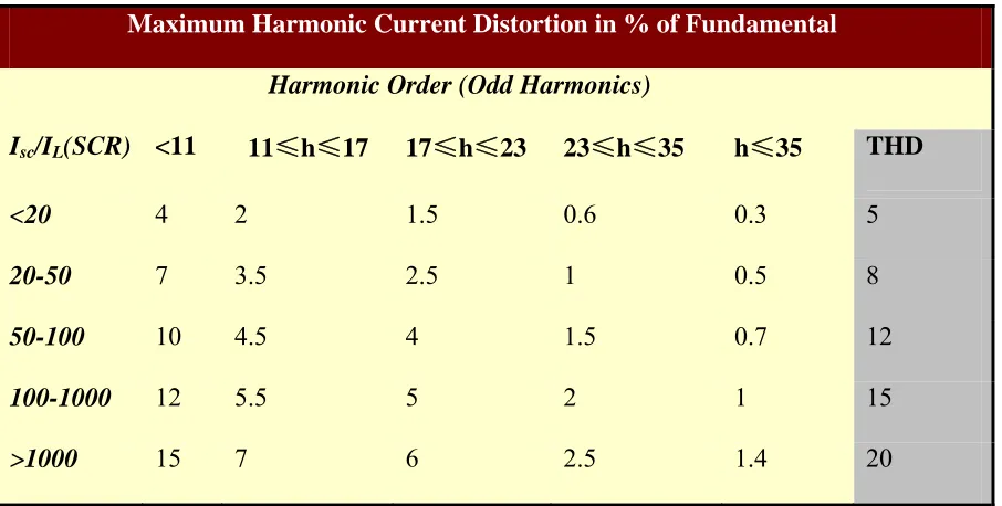
With the increased use of static power converter that require harmonic currents from power system, the Static Power Converter Committee of Industry Applications Society recognized the potential problem and started work on a standard that would give guidelines to users and engineer-architects in the applications of static power converter drives and other uses on electric power systems that contained capacitors. The result was IEEE 519-1981, IEEE Guide for harmonic control and Reactive Compensation of Static Power converters [4]. The IEEE 519 harmonic standard sets the limit on the Total Harmonic Distortion (THD) caused by the Non Linear Load at the Point of Common Coupling (PCC).Table I shows the harmonic current limits for Non Linear Loads at the Point of Common Coupling with other loads.
2
Maximum Harmonic Current Distortion in % of Fundamental
Harmonic Order (Odd Harmonics)
I
sc/I
L(SCR) <11
11
≤
h
≤
17 17
≤
h
≤
23
23
≤
h
≤
35
h
≤
35
THD
<20
4
2
1.5
0.6
0.3
5
20-50
7
3.5
2.5
1
0.5
8
50-100
10
4.5
4
1.5
0.7
12
100-1000
12
5.5
5
2
1
15
>1000
15
7
6
2.5
1.4
20
Where Isc=Maximum Short Circuit current at the Point of Common Coupling,
IL = Maximum Load current (Fundamental Frequency) at the Point of Common Coupling.
Table I suggests that the limitation on the harmonic current is based on the size of the consumer who is injecting the harmonic current and also on the size of the power system to which he is connected. If the size of consumer load is low with respect to power system, the larger is the percentage of harmonic current the consumer is allowed to inject into the power system.
1.1.b Control of Harmonics and their Impacts
Commonly employed solutions for harmonic problems are:
1. Modify the System Frequency response to avoid the adverse interaction with harmonic currents. This can be done by adding or removing capacitor banks, changing their sizes, adding shunt filters, inductors to detune the system away from harmful resonances.[5]
3
a. Passive Filters: A Passive filter consists of a Series/Parallel combination of an inductor, a capacitor and a resistor specially tuned to filter a particular frequency current. The impedance of L-C tuned filter is lower than the source impedance at a particular harmonic frequency in order to absorb that harmonic current. Passive filter have an advantage of low cost, are less complicated and have high efficiency. However, they suffer from a serious limitation that their performance gets affected significantly due to the variation in the filter component values, filter component tolerance, source impedance, and frequency of ac source [6, 8]. Also, they may cause series and load resonances in the system. In this scenario, harmonic currents can get amplified on the source side and cause serious distortion in the voltage[6].The passive filters also tend to get overloaded in case the load harmonics increase[8]. A stiff utility system poses greater difficulty for design of passive filter because sharp tuning and high quality factor are required to sink harmonic current [7]. A typical passive filter tuned for 5th and 7th harmonic applied to power system is as shown in
figure1.
4
b.
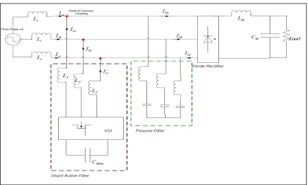
Active Filter: An Active Filter involves the use of one or more active components such as a Voltage Source Inverter which can be controlled in such a way so as to provide the compensating current or voltage to the nonlinear load. In this way, the nonlinear load does not draw the nonsinusoidal components from the source and thus the source becomes free of harmonics. Figure 2 shows a shunt active filter system used for providing the harmonic compensation so as to meet IEEE 519 Standard at the point of common coupling.The concept of shunt active filtering was first introduced by Gyugyi and Strycula in 1976[10]
.
Since then several Active Filter topologies have been proposed, some of them are: i) Shunt Active Filtersii) Series Active Filters
iii) Hybrid Parallel Active Filters
These topologies have been discussed in detail in the following chapters.
Major Advantage of Active Filter over Passive Filter is that it can be controlled to compensate for harmonics in such a way that THD lower than 5% at the Point of Common Coupling can effectively be achieved. The shunt Active Filter can also be made to act as a damping device in a parallel resonance circuit formed by the passive filter and the power supply system by adopting a lead function in its controller [9].Thus it can prevent harmonic propagation resulting from harmonic resonances. Briefly, Active Filters can be designed to achieve following three goals:
5
1.2 Thesis Objective
The main objective of this thesis is to develop a controller for 5 KVA Shunt Active Filter system. The shunt active filter system consists of a 5KVA Active Filter inverter, a harmonic extractor and a current regulator. The harmonic extractor is implemented using three different algorithms for harmonic current extraction for comparison. These are based on Load current, Supply current and Vf (Voltage at the Point of Common Coupling) harmonic extraction.
The current regulator is implemented using predictive current control method.
An Active filter inverter is required to be switched at higher switching frequencies (50-100Khz) so as to reduce the harmonic content at the point of common coupling to be typically lower than 5% as specified by IEEE 519 harmonic standard. An attempt has been made in this thesis to implement the harmonic extraction algorithm on an Analog Board, by using Field Programmable Analog Array (FPAA) and Field Programmable Gate Array (FPGA) and then comparing the delays in the implementation on each of them. Various advantages and disadvantages of each of the methods are also analyzed.
1.3 Outline
Chapter 2 gives a review of different active filter topologies like shunt active filter, series active filter, hybrid parallel active filter. All of these topologies are compared with each other based on the type of loads they can be applied for, required active filter rating and their control technique.
6
Chapter 4 discusses the implementation of Synchronous Reference Frame Controller using Field Programmable Analog Array (FPAA) and Field Programmable Gate Array(FPGA). It has been found that FPAA provide lower implementation delay as compared to FPGA and hence can prove a potential method for driving SiC based inverters at higher switching frequencies.
Chapter 5 discusses the hardware implementation of Shunt Active Filter System. Three types of loads have been used to validate the three harmonic extraction methods. This chapter also includes the experimental results from the predictive current controller board which receives its reference signal from the harmonic extraction board.
Chapter 6 gives the summary and the conclusion of the whole thesis work.
1.4 Glossary of Terms
PCC-Point of Common Coupling THD-Total Harmonic Distortion
FPAA-Field Programmable Analog Array FPGA-Field Programmable Gate Array SRF-Synchronous Reference Frame VSI-Voltage Source Inverter PWM-Pulse Width Modulation LPF-Low Pass Filter
HPF-High Pass Filter
7
CHAPTER 2. ACTIVE FILTERS
2.1 Review of Active Filter Topologies
2.1.a Shunt Active Filter
A Shunt Active Filter consists of a controlled Voltage Source Inverter (VSI) connected in parallel to the nonlinear load. A Shunt Active Filter compensates for the harmonic current required by the load so that the load only draws a fundamental current from the grid.
Figure 2.A Shunt Active Filter System
Therefore, for a Shunt Active Filter, according to the Kirchhoff’s current law at PCC, we can write the following equation:
8
component,
I
h.If the harmonic component is made equal to the compensation current,I
c,then only the fundamental current required by the load will come from the supply.The compensating current is supplied by the Active Filter Inverter which has a DC link capacitor. The capacitor voltage is held constant with the help of fundamental current from the grid.
In a practical implementation, a shunt active filter is always installed in parallel with a passive filter. The shunt passive filter, as shown in Figure 2, helps to absorb higher order harmonics and switching ripple. This helps the active filter to function with relatively smaller capacity [9].
A Shunt Active Filter Controller, whose design is discussed in detail in the following chapter, comprises of:
Harmonic Extractor-A Harmonic Extractor is required to generate a reference for the compensation current. A Harmonic Extractor tells us what harmonics we need to compensate for.
Current Regulator-A Current regulator compares the measured compensation current with the reference and produces the desired pulses for the Active Filter Inverter.
A Shunt Active Filter is suited for inductive or current source type load such as thyristor rectifier. If a Shunt Active Filter is used for voltage source type load then the injected current may be diverted to load causing its overloading [13].
2.1.b Series Active Filter
9
Figure 3. Series Active Filter System [10]
The voltages on the current sources are Vsa, Vsb, Vsc. The relation between the source voltage, the load
voltage and the active filter voltage is given by:
sa a ca
sb b cb
sc c cc
V V V
V V V
V V V
(2)
10
A Series Active Filter is suitable only for Capacitive or Voltage source type load such as condenser input type diode rectifier capacitive load [13].In case of series active filter, it is required to install a low impedance equipment such as LC filter or shunt condenser in parallel to the load is the load is of current source type or inductive [13].
2.1.c Hybrid Parallel Active Filter
Hybrid parallel active has an active filter in series with a particular frequency harmonic tuned passive filter .The main advantage of this Hybrid filter is that it reduces the VA rating of the active filter that needs to be installed in series with the passive filter. A practical active filter should have a VA rating lower than 5% of the load VA rating [11]. Hybrid Active filters improve compensation characteristics of the passive filters, making possible reduction in the active filter rating [11].This is done by making the active filter controller to implement a dynamically varying-either negative or positive ‘active inductance’. The controller produces the reference active filter inverter voltage which is then compared with the sine triangle to generate desired PWM pulses. The ‘active inductor’ inverter reference voltage, VLcmdn is given by [12]:
harmonic n inv cmdn Lcmdn
th
dt
di
L
V
(3)Where
L
cmdnis the positive or negative ‘active inductance’ to be synthesized at n
thharmonic frequency. It is the inductance which tunes Ln-Cn passive filter at nth harmonic frequency. Figure 411
Figure 4.Hybrid Parallel Active Filter SystemThe desired value of Lcmdn is determined by taking an error between the measured value of the nth
frequency component of filter current, ifn, and its reference ifn* and passing it through a PI
controller[as mentioned in [12].
12
CHAPTER 3.SHUNT ACTIVE FILTER CONTROLLER
The Active Filter controller consists of a harmonic extractor and a current regulator. In this chapter different methods of harmonic extraction have been discussed. Each method has its own advantages and is application based. Predictive current control technique has also been discussed in this chapter along with its implementation issues and the dead time compensation.
3.1 Harmonic Extraction
The harmonic extraction involves the process of determining all the multiple frequency components present in the current or voltage. The harmonics thus extracted become the reference for the current regulator. The current regulator thus produces pulses in order to drive the active filter inverter in such a way so as to generate the compensating current which is same as the reference.
The most common method used for harmonic extraction is Synchronous Reference (SRF) Frame method.
3.1.a Synchronous Reference Frame Harmonic Extraction
The Synchronous Reference Frame harmonic extraction method involves park transformation to convert three phase current or voltages into synchronously rotating d-q reference frame. The Park Transformation can be performed as follows:
c b a q di
i
i
Sin
Sin
Sin
Cos
Cos
Cos
i
i
2
1
2
1
2
1
)
3
2
(
)
3
2
(
)
3
2
(
)
3
2
(
3
2
(4)
13
component does not cause any phase error in the signal which might be an issue if a High Pass filter was used [14].
The Synchronous Reference Frame method of harmonic extraction can further be applied for load current, supply current and Vf (Voltage at PCC) harmonic extraction. All of these methods have been represented in the form of block diagram in Figure 5.
14
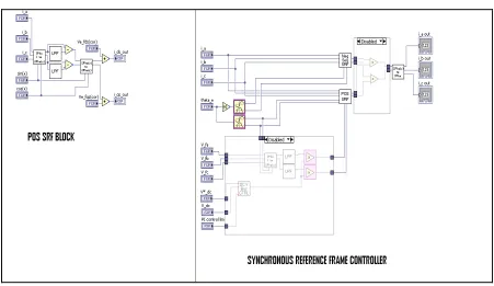
Figure 5.Block Diagram representation of Supply Current, Load Current and Vf harmonic extraction
15
The Load current harmonic extraction method is the feedforward method of compensation. In a load current harmonic extraction method, the THD cannot be improved beyond a certain extent as there is no controller gain which can be varied to improve the THD.
Supply Current Harmonic Extraction-
Figure 6 shows the equivalent circuit of an active filter. The three phase supply side currents are first converted from three phase to d-q components in synchronous reference frame. They are then High Pass Filtered as discussed above to obtain high frequency components. As derived in [9],Ic=G(s)*Ish
(5)
Where Ic=Compensating Current, Ish=Harmonics present in Supply Current, G(s)=Active Filter
Control Function.
Figure 6.Harmonic Equivalent Circuit of Active Filter
16
1
)
(
)
(
)
(
s
T
s
KT
s
G
(6)Ic=
1
)
(
)
(
s
T
s
KT
*Ish (7)
Also, Vf =s(Ls)*Ish (8)
Substituting (8) in (7),we get
Ic=
s K L KT
Ls s
1
*V (9)
Where Ls= Supply Side Inductance, T=Time constant of Lead Function, K=Gain Constant of Active
Filter Control Function, s=Laplacian Operator
Equation (9) shows that an active filter behaves as a series circuit of a resistance of Ls/KT and an
inductor with inductance of Ls/K equivalently. Figure 7 shows the lead plus proportional
characteristics of an active filter controller. This figure helps us to choose the value of K=5.
17
The supply current harmonic extraction method is a feedback method of compensation and
implements a gain which can be varied to improve the THD. The supply current harmonic extraction method provides the source to load harmonic isolation.
V
fHarmonic Extraction Method-
Harmonic propagation is a serious phenomenon in powerdistribution systems. This occurs due to the harmonic resonance between line inductors and capacitors which are installed for power factor correction. Also, it has been pointed out by actual measurements that fifth harmonic voltage at the end bus is magnified by 3.5 times as large as that at the beginning bus in a 6.6kV, 17 km long power distribution feeder having capacitors with a total capacity of 245kVA [10].Therefore, installing active filter on the last bus makes it possible for active filter to damp out harmonic propagation [10]. In the Vf harmonic extraction method, G(s) =(KT)s. This provides lead characteristics to the active filter controller [9]. Thus,
Ic=(KT)s*Ish (10)
Substituting (8) in (10), we get
f v s f
c
K
V
KT
L
V
I
*
(11)Equation (11) means that active filter acts as a pure resistor of Ls/KT. In this way, an active filter can
be made to act as a harmonic damper by providing low impedance path to the harmonic frequencies. Vf method also provides the harmonic isolation between the source and the load. Vf method is the
feedback method of harmonic compensation. It has a gain Kv which can be varied to improve the
compensation and make the harmonic voltage at the PCC to go to zero. The limitation of the Vf
method comes into picture when the supply voltage contains the harmonics. In this case the Vf
18
harmonics. Also, by making the harmonics at the point of common coupling zero, the Vf method
causes harmonic current to flow from source to the load.
P-Q Theory
(IRP Theory) Method
-The P-Q Theory or Instantaneous Reactive Power Theory was first introduced in 1983 by Akagi, et al. In this method, A shunt active filter controller senses the three phase voltage at the point of common coupling ;Vfa, Vfb, Vfc and the three phase load currents;iLa, iLb, iLc. P-Q Theory first transforms sensed three phase voltages and currents into two phase
orthogonal axes, αβ system according to the following equations.
1 1
1
2 2
2 3 3
0
3 2 2
1 1 1
2 2 2
L a L b L c i i i i i (12) 1 1 1 2 2
2 3 3
0
3 2 2
1 1 1
2 2 2
f a f f b f f c V V V V V (13)
P-Q theory is based on the instantaneous power calculation in αβ coordinate system [10]. The instantaneous power is further divided into instantaneous real power, P and instantaneous imaginary power, Q. Both of these can be further divided into their ac and dc components as follows:
ac dc
P
P
P
(14)ac dc
Q
Q
Q
(15)Pdc and Qdc are referred to as the average components of real and imaginary powers and generally
represent the active and the reactive power consumed by the load respectively. Pac and Qac represent
19
because of the presence of harmonics in the system. They represent an additional power flow in the system without effective contribution to the energy transfer from source to load or from load to source [10]. The instantaneous value of P,Q can therefore be calculated as follows[10],[15]:
L f f
f f L
i
V
V
P
V
V
i
Q
(16)2 2
1
L f f
f f
L f f
i V V P
V V
i V V Q
(17)
Similarly, we get [from 15]:
2 2
1
c f f c
f f
c f f c
i V V P
V V
i V V Q
(18)
Where Pc and Qc are the instantaneous real and reactive power consumed by the compensator (the
active filter inverter). For the compensator to act as purely a harmonic compensator Pc = -Pac, Qc=-Qac.
It is found for the system having diode rectifier front ends that Pac ≈ 0[15].Thus, the equation for the harmonic compensator becomes:
2 2
0 1
c f f
f f
c f f c
i V V
V V
i V V Q
(19)
Where icα,icβ are the α-β components of the compensating current.
3.2 DC Bus Voltage Control
The Block Diagram representation DC Bus Voltage controller implemented for an active filter inverter is shown in Figure 5.The DC bus voltage is measured and its error with the reference DC bus voltage is passed through a PI controller to get the desired current command. This current command is then multiplied with the fundamental component of the Voltage at PCC, Vf. This is done in order to
20
reference compensating current, Ic*.The measured DC bus voltage has to be low pass filtered to
attenuate ac components present in Vdc. The dominant components of DC Bus voltage are at multiples
of 360 Hz. These are present on the DC side because of the presence of 5th and 7th harmonic
components on the ac side of the inverter [14]. If these harmonics in Vdc are not attenuated, they
might generate harmonic reference in order to eliminate these harmonics from Vdc and in the process
they will affect the actual harmonic reference current. Further, in the presence of supply voltage distortion active filter terminal voltage harmonics will interact with the DC bus voltage controller generated reference harmonic currents. This will result in a real power transfer between supply and dc bus. Thus, filtering ensures that the power transfer between the supply and dc bus only takes place at the fundamental frequencies [14].
3.3 Current Controller
3.3.a Predictive Current Controller with charge error control
Predictive Current controller with charge error control has been used for non-sinusoidal current tracking. The Current controller should be designed for a multiple frequency current tracking as opposed to a single frequency current tracking as may be in the case of motor drives. It should have an ability to operate with lower active filter inductance, Lf. A lower value of Lf allows better di/dt
tracking and higher current bandwidth. It should have lower sensitivity to Lf and Vf estimation error.
It should provide a simple and a cost effective implementation in analog domain [20].
21
A predictive current controller has been proposed in [14] to address these issues. While designing predictive current controller, it has been assumed that the reference current remains constant over the complete switching period. Also, to eliminate low frequency errors, high frequency averaging has been performed per switching period such that the charge error over one switching period is equal to zero.
It has been shown that by using Space Vector PWM method, this high frequency averaging can be applied. In this method, the active space vectors are centered and hence the zero vectors are implicitly defined. This placement of the space vector minimizes the harmonics per switching period [14]. The schematic diagram of the implementation of predictive current control in analog domain has been shown in Figure 8.As can be seen from this figure, the predictive current controller with charge error control has been implemented in Stationary reference frame (or ds-qs frame).This achieves decoupling
of phases and alleviates the concerns of phase interactions and limit cycles in the active filter current, if. Decoupling of phases also ensures predictable peak to peak current ripple for a given dc bus
22
Figure 8.Predictive Current Controller with charge error control (Reproduced from [14]) The equations that describe current controller operation are:
*
fqs fqs fqs i i
i
(20)
*
fds fds fds i i
i
(21)
) ( 2 0 dt i T WT i T L V sw T fqds sw fqds sw f
xqds
(22)fqds xqds invqds V V
23
Where,
i
fqs and i*fqsare the q components of active filter compensating current and its reference current respectively; Vinvqds* is the reference inverter voltage in stationary reference frame;V
fqdsis the active filter terminal voltage(or the voltage at PCC) in stationary reference frame. As can be seen from Figure 8, the inverter reference voltage is produced by the sum of two parallel paths. In the first path the current error, ΔIfqds, is sampled every half switching period to improve tracking of higherorder harmonic current due to their reference change within one switching period. This sampled current is then multiplied by Lf/(Tsw/2) and then added to the back emf Vfqds to generate the reference
active filter inverter voltage as in a conventional predictive current controller.
In the second parallel path, the integral of the current error or the charge error is determined and reset every switching period Tsw. This is achieved by an integrator reset and a sample and hold circuit. If an
integrator is allowed to run free, it might accumulate low frequency errors and may cause integrator saturation problems. The weighting factor or WT as shown in the figure is to make the high frequency current averaging over a window greater or lesser than one switching period. A WT=2 means the current averaging over half a switching period [20].
The charge error is converted back to an equivalent Δichargeqds by dividing it by Tsw. This is then added
to the sampled value of Δifqds and their sum is multiplied by Lf/(Tsw/2) to produce the reference
voltage across the inductor Lf. This is then added to the back emf Vfdqs to produce the inverter
reference voltage,Vinvqds* [20].
3.3.b Space Vector PWM and its implementation in Analog Domain
24
consecutive switching vectors in proximity to the reference helps to reduce the number of switching operations required and thereby helps in the reduction of switching losses. The space vector PWM generation method is regarded as the “superior” PWM generation technique [15] as compared to Sine-PWM technique which is implemented by comparison of reference with a sine triangle. Figure 9 shows the block diagram of the analog implementation of the space vector PWM technique.
It has been shown that on injecting triplens to the reference waveform and then comparing it with the triangular waveform produces the same switching pattern as is does by space vector PWM technique. Therefore, the inverter reference voltage in stationary α-β reference frame is transformed into the three phase inverter reference voltages; *
,
*,
*invcn invbn invan
V
V
V
.The extraction of triplens is achieved by passing three phase inverter reference voltages through a diode bridge circuit. This circuit extracts the maximum of the three during positive cycle and minimum of the three during negative cycle thereby resulting in the triplen extraction. The triplens are then added to the reference voltages. This resulting space vector modulating waveform; Vmoda, Vmodb, Vmodc is regularly sampled and synchronized to the25
Figure 9. Block diagram of the Analog Implementation of the Space Vector PWM Technique
3.3.c Implementation issues and Dead Time Compensation
26
respect to the sampling pulse, such that both the sampling and the switching take place at the same instant. This method has been implemented in this work.
The other method for the dead time compensation is the feed forward method in which the compensation is provided by adding/subtracting the feed forward voltage depending upon the sign of the measured inverter current [20].
3.4 Bandwidth of Active Filter Inverter
The bandwidth of an active filter inverter is the range of frequencies which an inverter can produce at its terminals. It is decided by the frequency at which the inverter is switched and the inverter DC bus voltage. An active filter is required to compensate for multiple harmonics to achieve a THD which is typically lower than 5% (for SCR<20).Not only this, the remnant high frequency/high slew rate component in the supply current which is present even after compensation can lead to a very high voltage induced across the inductor. Therefore, in order to compensate for these higher order harmonics, there is a need to switch active filter inverters at a very high frequency. In this work, the switching frequency, fsw=20Khz.
3.5 Active Filter System Specifications
The Active Filter System Specifications taken for the purpose of designing the Simulink Model are: Vs= Line to Line Supply Voltage = 460 V rms
Ls= Supply Side Inductance=22µH
Ldc=DC Load side inductance =340µH
Cdc=DC Load side Capacitance=30mF
Lf=Filter Inductance=75µH
Cdcbus=DC Bus Capacitance=12.5mF
27
Parallel Passive Filter Specifications (for20khz switching frequency) (taken from [14]) Parallel Passive Filter circuit used in the simulation is as shown in Figure 10.
Figure 10.Parallel Passive Filter system used in Simulation LT=21µH
CT=3µF
RT=50mΩ
C=50µF Rd=1.7Ω
3.6 Simulink/MATLAB Model and Simulation Results
3.6.a Simulation Results of System without Active Filter
28
Figure 12.Supply Current waveform for the system without active filter
Figure 13.FFT Analysis of the Supply Current Waveform for the system without Active Filter From the simulation results it can be seen that the System having Non-Linear load has :
Total Harmonic Distortion=28.68% 5th Harmonic Content=22.74%
29
11th Harmonic Content=8.29% 13th Harmonic Content =6.01%
Figure14. Vfa(l-n Voltage at PCC) of the system without active filter
3.6.b Active Filter Compensation using Supply Current Harmonic Extraction Method
30
Figure 16.Supply Current waveform after the active filter compensation using supply current harmonic extraction method
Figure 17.FFT Analysis of Supply Current Waveform after compensation
31
Figure 18.Compensation current matching with the Load Current Extracted Harmonics
32
3.6.c Active Filter Compensation using Load Current Harmonic Extraction method
Figure 20.Simulink Model of the Active Filter Controller using Load Current Harmonic Extraction Method
33
Figure 22.Supply Current Waveform after the active filter compensation using load current harmonic extraction method
Figure 23.FFT Analysis of Supply Current Waveform after compensation
The FFT Analysis of supply Current waveform after the active filter compensation using load current harmonic extraction method shows that:
34
Figure 24.DC Bus Voltage Controlled at 680V3.6.d Active Filter Compensation using Vf (Voltage at PCC) Harmonic Extraction
method
Figure 25. Simulink Model of the system with active filter controller using Vf harmonic extraction
35
Figure 26.Supply Current Waveform after compensation using Vf harmonic extraction method
Figure 27.FFT Analysis of Supply current waveform after harmonic compensation using Vf harmonic
36
The FFT Analysis of supply Current waveform after the active filter compensation using Vf (Voltage
at PCC) harmonic extraction method shows that: Total Harmonic Distortion=3.34%
The value of Kv chosen for this simulation =140.
The Table below shows the total harmonic distortion (THD) that we get from the FFT Analysis of supply current waveform for different values of Kv. It is clear from this table that on increasing the
value of Kv, we achieve better THD. This is due to the fact that on increasing the value of Kv, the
resistance implemented by active filter reduces and hence it offers a low impedance path to the harmonic frequencies thereby resulting in better THD.
Table II. Effect of Change in Kv on Total Harmonic Distortion (THD) of supply current waveform
K
v Total Harmonic Distortion(THD)37
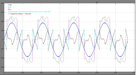
Figure 28. Compensating current, the harmonic current extracted from load current and Vfa
Figure 29. DC Bus Voltage Controlled at 750 V
3.7 Comparison between the three different harmonic extraction methods
38
inductance and resistance realized by the supply current harmonic extraction method can be varied to get low THD. The supply current harmonic extraction method is especially important when the source voltage has harmonics as this method directly aims to reduce the supply current harmonics to zero. Also, the supply current harmonic extraction method can provide a good suppression of amplification of harmonic currents due to anti parallel resonance.
The Vf harmonic extraction method is a feedback method of compensation which provides
proportional characteristics to the active filter controller. The equivalent resistance realized by the active filter controller makes the active filter to act as harmonic damper along with the harmonic compensator. This method is aimed at reducing the harmonic voltage at the point of common coupling to zero so that only the fundamental current is drawn from the supply. The main drawback of this method is in case when the supply voltage has harmonics. In such a case, reducing the harmonic voltage at the point of common coupling to zero can lead to an increase in the supply side harmonic current.
The load current harmonic extraction method is a feed forward method of compensation. It is the most simple and straightforward method of harmonic compensation. Though, in this method, the THD cannot be improved beyond a certain point as there is no controller gain which can be varied to improve THD. The load current harmonic extraction method can only make an active filter act as a harmonic compensator but not as a harmonic damper. It can also not provide any compensation in case the supply voltage has harmonics.
39
3.8 Summary
This chapter discusses in detail about the three harmonic extraction algorithms and the predictive current control technique. The simulation results have been presented to verify the control algorithms and to make comparisons between them. All the three harmonic extraction method have been shown to give a THD <12% (for Ls=22µH,SCR=50-100) thereby conforming with IEEE 519 harmonic
standards. From the simulation results, in terms of achieving low THD, it can be inferred that Vf
(Voltage at PCC) harmonic extraction method gives a better harmonic compensation (THD=3.34%) as compared to the supply current (THD=6.24%) and load current (THD=3.82%) harmonic extraction method. From the comparison between three methods, it has been found that each method has its own specific use. All the methods can provide a good harmonic compensation, in terms of conforming to IEEE 519 harmonic standards, but it depends upon the need of the system (in terms of requirement of harmonic damping or compensation of harmonics present due to supply voltage) to be able to choose which method to use.
40
CHAPTER 4. FPAA AND FPGA IMPLEMENTATION OF SRF CONTROLLER
The presence of multiple harmonics in the power line due to various non-linear loads like adjustable speed drives, computers, fax machine, PLC’s, etc. requires high frequency switching of an active filter inverter so as to reduce the harmonic content at the point of common coupling (PCC) to be typically lower than 5%(for SCR<20) as specified by IEEE 519 harmonic standards. In this work, the Field Programmable Analog Array (FPAA) based analog controller has been used to implement the SRF Controller algorithm for harmonic current extraction for Shunt Active Filter controller and the results are compared with the conventional digital implementation on Field Programmable Gate Array (FPGA). The FPAA based analog controller implementation proves to be faster than the digital FPGA implementation and can be a potential controller for SiC based active filter inverters with high switching frequencies of 50-100 kHz (10-20us).4.1 Field Programmable Analog Arrays
41
Figure 30. FPAA Configuration Diagram [16], [17]FPAA’s are reconfigurable and easy to design and can simulate complex analog circuits as compared to Analog Boards. They are also much faster than Field Programmable Gate Array (FPGA) in terms of speed while delivering the results with same accuracy. In FPGA’s the additional delay can be attributed to Analog to Digital and Digital to Analog conversion steps. Thus, FPAA’s provides not only the ease of reconfigurability of complex analog circuits but also proves to be the best solution when it comes to high speed switching applications.
42
Figure 31. Anadigm’s AN231E04 FPAA Evaluation Board
4.2 Simulation Results of Positive Sequence SRF Controller Using Simulink/MATLAB
The simulation of Positive sequence SRF controller with square wave input as the harmonic current waveform has been performed and the results are shown below.Figure 32. ILa,ILb,ILc waveform input to the SRF Controller
Figure 33. e Lq e Ld
I
I
,
waveform obtained after the Park Transformation e Ld I43
Fig34.e Ld e Lq
vs
I
I
Figure 35. s hq s hdI
I
,
waveformsIdeally,
I
hds should coincide with ILa at each zero crossing as shown in the Figure 36 below.
Figure 36. Ihd and ILa waveform
4.3 Implementation of SRF Controller on FPAA
The Positive sequence SRF Controller has been implemented using seven AN231E04 boards.
The FPAA chips are configured using Anadigm Designer 2 software. Figure 37 shows the
implementation of SRF Controller on seven FPAA boards using Anadigm Designer 2
s hq I s hd
I
Point at which both waveforms coincide ideally
44
software. The corresponding
experimental setup is shown in Figure 38.A 3rd order Butterworthfilter with a cutoff frequency of 10Hz has been implemented to perform a low pass filter operation on FPAA.
Figure 37. Implementation of Positive Sequence SRF Controller using Anadigm Designer 2 software
45
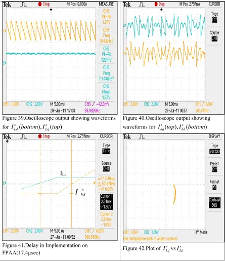
Figure 39.Oscilloscope output showing waveforms forI
Lde(
bottom
),
I
Lqe(
top
)
Figure 40.Oscilloscope output showing waveforms for
I
hqs(
top
),
I
hds(
bottom
)
Figure 41.Delay in Implementation on
FPAA(17.4µsec) Figure 42.Plot of
e Lq
I
vs eLd I
From these results, it can be seen that the delay in implementation of the complete positive sequence SRF controller algorithm is 17.4
µsec.
s hd
I
46
4.4 Implementation of SRF Controller on FPGA
The National Instrument Compact-RIO (NI-C-RIO) digital controller system consists of a reconfigurable chassis that contains the user programmable FPGA, hot swappable I/O modules and a real time controller. LABVIEW software is used to program the FPGA and the digital NI-CRIO controller system. The square-wave (worst case for harmonic current extraction) load currents iLa, iLb,
iLc were generated by the C-RIO controller internally and then provided as inputs to the programmed
SRF Controller. A 4th order Butterworth filter with a cutoff frequency of 10 Hz has been used to perform a low pass filter operation. The outputs of the FPGA (C-RIO) controller which are
I
ha,
I
hb,
I
hccompensating harmonic currents extraction are shown in Figure 44. It is verified that the digital FPGA based C-RIO controller can also be used to implement the SRF Controller – albeit with larger computational delays compared to an analog based FPAA controller implementation.47
Figure 44.Oscilloscope output showingwaveforms for Iha,Ihb,Ihc
Figure 45.Delay in Implementation on C-RIO(30µsec)
4.5 Comparison of Analog FPAA and Digital FPGA Controller Outputs
The comparison of the analog FPAA and digital FPGA based controllers were based on the implementation delay for the same SRF Controller based compensator for harmonic current extraction with exactly the same square-wave (worst case for harmonic current extraction) load currents iLa, iLb, iLc generated by the C-RIO controller for both analog (FPAA) and digital (FPGA)
controllers. The delays were measured by calculating the time difference between the zero crossings of two points (one point on the input signal, iLa and the other point on output signal,
I
hds ). These points of the two signals were chosen because the zero crossings of the input current signal, iLa andthe output current signal, s hd
I
are ideally supposed to coincide. Figure 41 shows a time delay of 17.4μs for the implementation on analog FPAA based controller. Figure 45 shows a time delay of 30μs for the implementation on digital FPGA based controller. Thus, it can be seen from the results obtained from both the implementations that the FPAA analog controller is much faster than the48
49
CHAPTER 5.HARDWARE IMPLEMENTATION OF SHUNT ACTIVE FILTER
SYSTEM
The hardware implementation of shunt active filter system has been performed by first building a nonlinear load (for lower power rating as compared to the simulations shown in Chapter3) in the laboratory. The current and the voltage measurements from the nonlinear load were then given to the harmonic extraction board and the current controller board to drive the active filter inverter.
Figure 46 shows the hardware setup of the shunt active filter system in laboratory.
Figure 46.Hardware Setup of Shunt Active Filter Controller and the Nonlinear Load
5.1 Nonlinear Load Specifications
Vs(rms line to line)=208V
Ls=Supply Side Inductance=2.5mH
Harmonic Extractor
Predictive Current Controller
Non Linear Load
50
Lac=Smoothing Reactor =2.5mH Ldc=DC side Inductance=5mH Cdc=DC side Capacitance=50µF Rdc=DC Load=72Ω
Pdc=Load Rating=944.67W
Rstartup=Startup Resistance=5Ω,100W
5.1.a Diode Rectifier with DC side Inductor, and DC side Capacitor system
This type of nonlinear load has a higher value of di/dt for the supply current waveform. The dc side inductor has the effect of increasing the di/dt of the supply current waveform but reducing the supply current amplitude ripple. The amplitude of the ripple depends on the value of Ldc chosen. Particularly,
for the specifications of this system, the value of Ldc is such that it gives a discontinuous supply
current waveform.
51
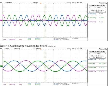
Figure 48. Oscilloscope waveform for Scaled Isa,Isb,IscFigure 49. Oscilloscope Waveform for Scaled Three phase voltage Vfa,Vfb,Vfc
5.1.b AC Supply Side Line Inductor and Diode Rectifier with DC side Capacitor system
52
Figure 50. Diode Rectifier with AC supply side Inductor and DC side Capacitor system
Figure 51. Oscilloscope waveform for Scaled Isa,Isb,Isc
53
5.1.c AC Supply Side Line Inductor, Diode Rectifier with DC side Inductor, and DC
side Capacitor system
The Nonlinear Load schematic for AC Supply Side Line Inductor, Diode Rectifier with DC side Inductor, and DC side Capacitor system is shown in Figure 53.This is the most desirable utility interface topology for ASD’s and other loads like DC power supplies. The supply side AC line inductors reduce the THD and the di/dt of the supply current waveform [18]. Also, Ldc helps in
getting a continuous supply current and helps reduce supply voltage unbalance effects on supply side [18].
The Diode Bridge startup circuit is required to limit the inrush current due to the charging of DC side capacitor during start up. For this purpose, a startup resistance is used in this circuit and all the other nonlinear load circuits shown above for initial few seconds and then it is taken out of the circuit using a switch as shown in the figure.
54
Figure 54.Oscilloscope waveform for Scaled Isa,Isb,Isc55
Figure 56.Fast Fourier Transform (FFT) of the Isa waveform on oscilloscope
5.2 Harmonic Extraction on an Analog Board
The harmonic extraction board has been implemented on an analog board using integrated circuits. Three different harmonic extraction algorithms have been implemented namely Vf, Load Current and
Supply current harmonic extraction method as discussed in chapter 3.The board receives the voltage and current signals measured from the nonlinear load system and gives out the extracted harmonics in αβ stationary reference frame and the three phase. These extracted harmonics become the reference
56
Figure 57.Magnitude Bode Plot of the 5th order Butterworth Filter (Gain Normalized to the Cut off Frequency) (Reproduced from MAX280 Datasheet)
5.2.a Implementation delay of Analog harmonic extractor
The analog harmonic extractor board has an implementation delay of 4.8µsec.The delay is measured by using the input currents ILa , ILb, ILc as the currents of 7th harmonic frequency. The extracted
![Figure 30. FPAA Configuration Diagram [16], [17]](https://thumb-us.123doks.com/thumbv2/123dok_us/1305728.1163217/58.612.93.539.69.282/figure-fpaa-configuration-diagram.webp)