Technology (IJRASET)
Silicon Wafer Technologies: Past & Future
Mr. Nitesh Kumar Dixit1, Ms. Abhilasha Agarwal2, Ms. Malvika Purohit3
1,2,3
Department of Electronics & Communications, BIET Sikar
Abstract: Silicon is now best substrate material for IC technologies. This paper is review about development of wafer technologies in past and future. Also discuss about silicon crystal growth, Silicon on Insulator technologies and CMOS devices capabilities. The roadmaps of industry manufacturing and future of silicon wafer technologies also discuss.
Keywords: Silicon, Crystal Growth, Roadmap, CMOS, Wafer Technology.
I. INTRODUCTION
Silicon is base material for Integrated circuit preparation. Silicon covers 90% of market of IC fabrication. It has several advantages
than any other semiconductor like larger band gap, higher operating temperature, easily available and converted easily into SiO2.
The SiO2 layer is effective insulator that helps to make stable structure of ICs. For application purpose, silicon is most adequate
material, market also feeding more and more devices to silicon wafer. In 2010, silicon wafer production and sale was around $10 billion [1]. But some issues like active power dissipation, high leakage current etc. are limits the use of silicon, to overcome these problem replace the silicon with other materials. To increase higher band gap and breakdown voltage gallium nitride (GaN) grown on silicon surface, to increase operating frequency source/drain of MOSFET made by SiGe Cu used metallization.
In nature, Silicon is found as an oxide in the form of sand and Quartz. For fabrication process, Silicon must be in crystalline form i.e.
very pure free from defects and uncontaminated. In general, 1022 atoms per cubic cm in silicon and therefore we require not more
than one unwanted impurity on 109 silicon atoms[2]. This is a purity of one atom in a billion.
As we know that silicon as an element is not found in nature it is found as silicon dioxide in the form of quartz sand. There are several methods for obtaining pure silicon one of them is to first refine silicon dioxide with carbon in an arc furnace at very high
temperature [3]. Which gives Si and Co2. Than Co2 evaporate as a gas and leaving behind impure silicon which is known as
metallurgical grade silicon. Now next step to purify the silicon for that first we produce silicon tetra chloride by burning the silicon. Si + 2Cl2 SiCl4
SiCl4 + H2 Si HCl3 + HCl
Now this tri chloride is reduced by hydrogen to form very pure silicon which is known as Electrode grade silicon. EGS to produce a single crystals of silicon. It can be done by a method known as crystal growth.
II. SILICONSUBSTRATEMATERIALSTECHNOLOGY
An easy way to comply with IJRASET paper formatting requirements is to use this document as a template and simply type your text into it. In the 1950s, Crystal growth and substrate technologies are speedily evolving to become a specialty producing platform which will address the distinctive wants of the star business. Whereas elementary processes within the producing of element wafers are in situ, element producing technology has unendingly improved so as to satisfy the element wafer constant quantity capability and value necessary to sustain scaling progress on semiconductor and star business roadmaps [1]. Producing strategies ordinally employed in the business are made public in Fig. 1 and also the key aspects for varied processes are represented within the following sections. In the 1950, crystals were grownup principally by the float zone (FZ) method and wafers were engraved once diamond sprucing. However within the 1960, abundant of the elemental work for the present element business was initiated [2].
A. Production of Polysilicon
Technology (IJRASET)
[image:3.612.86.523.82.340.2]Fig 1: IC Development process (a) Silicon Development (b) Silicon Wafer Development (c) Layer Growth (d) Final Packaging
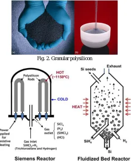
Fig. 2. Granular polysilicon
[image:3.612.176.440.373.697.2]Technology (IJRASET)
This technique utilizes heated silane and element gases, that are injected into very cheap of the reactor inflicting a bed of tiny element seed granules to become fluidized. The silane decomposes within the hot reactor and element is deposited on the seeds inflicting them to grow in size and weight. Once grownup to the specified size, the granules (Fig. 2) are extracted from very cheap of the reactor whereas recent seed particles are fed into the highest of the reactor. Fluidized bed reactors utilize nearly all the silane gas fed into the reactor, offer superior heat and mass transfer characteristics, and are energy economical [2]. As highlighted in Fig. 3, FBR method is additionally endless method whereas the Siemens method could be a batch method. Thus, the FBR method is a more economical than the Siemens method and is changing into a lot of wide adopted. Electronic grade polysilicon has impurities within the low elements per billion (ppb) vary or less, which is a necessary demand for production of semiconductor devices.
B. Growth of Single Crystal element
The business commonplace for production of monocrystalline element for semiconductors is that the Czochralski (CZ) methodology. Use of melt-based growth for semiconductor crystal growth was pioneered by Teal and small by demonstrating the expansion of single crystal Ge [3], [5]. Later, Teal and Buehler grew CZ–Si victimization constant technique, however they may solely grow injured single crystals of specific orientation [6]. The primary demonstration of dislocation-free CZ element crystal growth was incontestable in 1959 by Dash, employing a changed seeding technique [7] [8]. Growth of element crystals by the CZ methodology has been wide studied over the course of the subsequent 5 decades as shown in fig. 7. Dislocation-free, high-purity element crystals up to 450 metric linear unit in diameter are currently potential on a poster scale.
A great deal of effort was exhausted on distinguishing, characterizing, and reducing impurities within the CZ growth method, notably carbon, oxygen, and boron, that were at a lot of higher levels than those of FZ Si, and caused issues in sure device applications. With diligent effort and therefore the advent of low polysilicon from the Siemens method, the impurity levels of CZ were greatly reduced, and therefore the CZ method displaced the FZ method all told however a couple of specialty applications.
Fig 4. Czochralski crystal growth (a) meltdown; (b) seed dip; (c) top; (d) shoulder; and (e) body
C. Crystal Cropping and Grinding
Technology (IJRASET)
[image:5.612.93.521.306.499.2]the flat was replaced by a notch. D. Slicing the wafer production method (Fig. 5) starts with slicing of the crystal metal bar. Second styles of slicing ways are employed in the Si wafer industry i.e. the inner diameter (ID) saw and the wire saw. The ID saw uses a skinny ring-shaped blade with a diamond guaranteed region on the within fringe of the annulus. ID saws cut only 1 wafer at a time, taking a couple of minutes to slice every wafer from the crystal. Blade flexure throughout slicing light-emitting diode to warp and bow within the ensuing wafers and blade wear or poor blade dressing resulted in higher total thickness variation (TTV) from the saw. High TTV from the saw should be corrected by the downstream processes. Law makers worked on the matter of developing tensioning systems to regulate flexing of the ever agent blades needed to scale back kerf losses. A wire saw on the opposite hand takes many hours to chop through a crystal metal bar, however makes many hundred parallel saw cuts at the same time, wafering the complete metal bar in one operation. At crystal diameters larger than one hundred fifty millimetre, wire saws have established to be a lot of economical than ID saws with higher output and therefore the potential for lower kerf losses by exploitation agent wires. Machining processes that turn out sleek flat polished surfaces usually have low throughputs and thus are dearer for a given capability demand as a result of a lot of machines are needed that successively needs more room on the mill floor, a lot of maintenance, and doubtless a lot of operators [10]. High output machines on the opposite hand cannot reach the surface quality needed for semiconductor wafers. As a result, a mix of machining processes is employed within which the initial processes are quick, rough cuts and ulterior steps use slower cuts to get rid of the harm from previous steps while not causation new harm. The fundamental sequence of steps is shown in Fig. 1(b) beginning with edge identification that applies a formed wheel to make a rounded wafer edge profile that is a lot of immune to breaking.
Figure 5. Sequential process of Silicon wafers manufacturing.
D. Lapping and Etching
As-cut wafers from a saw usually have a better TTV than that needed for progressive planography processes employed by device makers. This state is corrected by subjecting the wafers to a grinding (fixed abrasive) or covering (loose abrasive) method. The macroscopic flatness of wafers is often determined by this covering or grinding method [11]. Succeeding chemical etching removes the crystallographic injury that these processes manufacture however care should be taken that this etching not degrade the flatness. This is often achieved through selection of the etching chemistry, careful style and operation of the etching tanks, and therefore the fluid mechanics of the etchant flow. Etchants embrace caustic etches like KOH, that leave a comparatively rough surface however maintain a really high degree of macroscopic flatness or acid print, which may be optimized to provide a sander surface however far more seriously degrades the macroscopic flatness particularly close to the wafer edge [12]. The active elements of acid etching square measure hydrofluoric and azotic acids in either carboxylic acid or oxyacid, that square measure accustomed tailor the viciousness. If utilized in the proper manner and in appropriate tanks, acid etching will manufacture a sleek, shiny surface.
Technology (IJRASET)
surface was ironed onto a rotating polymer pad soaked within the oxide suspension [11]. Developments over 5 decades embrace reduction in particulate contamination, which may cause scratches, coming up with sharpening machines with higher stability, understanding and rising pad wear mechanisms and pad dressing procedures yet as optimizing pressures, temperatures, and flow rates to optimize flatness. Suspension chemistry has additionally been improved with varied additives to extend removal rates and increase chemical purity to avoid undesirable metals like copper.
F. Cleaning
A clean chemical element surface is important to device performance. Contaminants will cause discharge, low breakdown voltage, no uniform compound growth, lithography errors, and plenty of different issues for device makers [11] [12].
The key phases in improvement a chemical element surface are:
1) Removal of insoluble organic contaminants with a 5: 1:1 binary compound: H2O2: NH4OH solution
2) Stripping of a skinny oxide layer employing a diluted 50:1 H2O: HF solution
3) Removal of ionic and serious metal contaminants employing a answer of 6:1:1 binary compound: H2O2 : HCl
4) Passivation of the extremely reactive blank, clean, chemical element surface in binary compound.
G. Epitaxy
During the primary 20 years of the semiconductor trade, most devices were designed on polished chemical element substrates, however as device densities inflated and CMOS architectures were adopted, epitaxial substrates became the popular selection
among advanced logic and microchip makers [12]. At above >1000 0C temperature epitaxial layer was growth from chlorosilanes
with vary high rate (2-4m/min) of deposition. This process control by transporting of gaseous phase precursors to surface. Epitaxy
also performed at low 600 0C temperature from trichlorosilane to dichlorosilane to silane, growth rate also slow and this process also
controlled through gaseous phase transport phenomenon.
III.ADVANCEDSUBSTRATETECHNOLOGIES
Technical challenges square measure several for each device and substrate suppliers, and as completely different solutions evolve, we have a tendency to see a divergence in device architectures and therefore the substrates upon that they're designed[1] [10]. Important challenges square measure highlighted within the 2010 Technology Roadmap for Semiconductors (ITRS) (see Table 1).
Technology (IJRASET)
A. 450-mm Substrates
Wafer diameter modification needs a coordinated effort of the whole offer chain, wafer makers, instrumentality makers, and device makers. Whereas from a technical purpose they don't seem to be any elementary barriers, engineering challenges are vital. For the wafer providers, massive crystal growers, crystal handling systems, thermal process instrumentality (epi, RTA, furnaces), new safety concerns, wafer handling instrumentality, and automation systems would require a major style effort on the far side simple scaling of earlier instrumentality generations. Uniformity of wafer parametric over a pair of the world can gift additional challenges for wafer and device makers and their instrumentality suppliers. To boot, the introduction of 450-mm wafers would require vital effort come to agreement at intervals the trade on a way to achieve economic viability of such substrates [13]. From the device makers’ stand, the economic presumption has historically been that the world of the wafer can double whereas the price of the process instrumentality can increase by a lesser quantity (30%) at roughly constant wafer turnout (except for lithography, metrology, and particle implantation, that account for ever larger shares of the entire process), leading to a lower device value on larger diameter wafers. For the wafer provider and therefore the instrumentality provider, the state of affairs is way totally different. For the wafer supplier, it takes a far larger volume of silicon, processed at associate inherently abundant lower turnout, to form an equivalent extent of silicon at larger wafer diameters than at smaller wafer diameters. Hence, the price per unit space of larger beginning wafer will increase for strictly physical reasons, even within the absence of monumental development and capital retooling prices which will be needed. For the instrumentality provider, a diameter increase incurs monumental style and development prices that should be recouped over a smaller put in base of tools. The matter of assignation of prices, risks, and come back on investment through the availability chain during a property fashion has over-involved the introduction of 450 metric linear unit, currently slated for 2014. At the terribly least, careful engineering value models can have to be compelled to be developed that area unit understood and in agreement to by the whole offer chain.
B. Silicon-on-Insulator Substrates
So far SOI wafers have remained solely tiny low fraction of the entire silicon market, primarily as a result of the price is considerably more than that of associate epitaxial wafer. In areas like MEMS, high voltage, optical waveguides, ultralow power, radiation hardened, and RF devices, the distinctive blessings of SOI justify the worth differential [1]. As capabilities improve and prices come back down, we must always expect the SOI wafer share to extend in alternative market segments. With continued scaling on the far side twenty two nm, the matter of Vth variations thanks to random dopant fluctuations (RDFs) within the channel implants accustomed management short channel effects could become intolerable, significantly for stable static random access memory (SRAM) operation [1][3]. The utilization of totally depleted SOI (FDSOI) transistors with undoped channels offers a possible resolution. However, the edge voltage of transistors designed around FDSOI technology may be an operate of the highest silicon layer thickness and at the 10–20-nm layer thickness needed, a 1-nm thickness variation corresponds to a couple of 25-mV variation in Vth, that places tight constraints on layer thickness uniformity. Management at these levels means the thickness uniformity demand is approaching the dimensions of typical surface peak to depression roughness for layer transfer technology. FDSOI are often combined with a 10–20-nm buried compound (BOX) layer [ultrathin body and BOX (UTB) transistors] to enhance short channel effects and open up the chance of dynamic threshold voltage management by applying back gate bias [33].
C. Looking on the far side ancient CMOS
Technology (IJRASET)
doubtless that different device manufacturers can adopt different solutions, and these solutions can doubtless need a spread of bulk and SOI substrate styles.
D. Integration With Compound Semiconductors
In several areas, silicon is probably going to be the bottom substrate for a few new materials integration. We have a tendency to area unit already seeing efforts to exchange sapphire or carbide with silicon for III-nitride materials [18]. whereas the barriers area unit formidable, thanks to thermal and lattice mismatches, some corporations area unit manufacturing GaN/Si substrates, that area unit at first finding use within the high-voltage power device market [19]. Further, tries area unit being created to enhance defect density to form them applicable for advanced devices like high brightness light-emitting diodes (LEDs) and lasers. In the end, every device manufacturer can realize the optimum resolution for its individual product combine in terms of value and performance and it looks doubtless that the solutions can vary across a spread of architectures and several other substrates. On the opposite hand, it looks quite bound that silicon in one kind or another can stay the semiconductor of selection for a minimum of another decade or 2 with various materials solely gaining share in niche segments of the semiconductor materials market.
IV.CONCLUSION
The drive for the electronics trade over the last forty years has been the relentless increase in integration density enabled by dimensional scaling and matched with the semiconductor device performance edges related to reducing metal–oxide–semiconductor junction transistor (MOSFET) essential dimensions [20]–[21]. The whole trade offer chain from material suppliers to instrumentality makers to device manufacturers have shared a standard trade roadmap that has charted the course for continued shrinking and inflated semiconductor device performance and chip practicality.
A more modern vital trend in semiconductor devices is that the inflated level of heterogeneous integration of numerous device varieties that add system practicality. Examples area unit the combos of ancient digital functions like central process unit (CPU) with non-digital functions like analog/mixed signal/RF, high voltage, passives, and sensors [22]. The mixture of those functions has generally been complete at the package level, however multiple functions area unit more and more combined in system-on chip approaches on single die. The trend for increasing integration of numerous device varieties to extend practicality has been represented as More than More [22] [23]. Silicon wafer styles can naturally vary for such a various set of device varieties. Wafer needs are determined way more by the device operate than by dimensional scaling.
V. ACKNOWLEDGMENT
We like to thank Mr. Jatasankar Punia, Vice Chairman of BIET, Sikar and Department of Electronics & Communications for their kind support.
REFERENCES
[1] The International Technology Roadmap for Semiconductors, 2009 ed., Dec. 2011. [Online]. Available: http://www.itrs.net/ home.html
[2] P. M. Petroff and A. J. R. de Kock, “Characterization of swirl defects in floating-zone silicon crystals”, J. Crystal Growth, vol. 30, pp. 117–124, Aug. 1975 [3] J. B. Little and G. K. Teal, “Production of germanium rods having longitudinal crystal boundaries”, U.S. Patent 2 683 676, issued Jul. 13, 1954, filed Jan. 13,
1950.
[4] J. Schurmacher, L. Woerner, E. Moore, and C. Ncwman, ‘‘The production of solar cell grade silicon from silicon bromosilanes,’’ NASA Jet Propulsion Lab., Pasadena, CA, DQE/JPL 9S4914-7812, Jan. 1979.
[5] G. K. Teal, M. Sparks, and E. Buehler, “Growth of germanium single crystals containing p-n junctions”, Phys. Rev., vol. 81, pp. 637–637, 1951. [6] G. K. Teal, M. Sparks, and E. Buehler, “Single-crystal germanium”, Proc. IRE, vol. 40, pp. 906–909, Aug. 1952.
[7] W. C. Dash, “Growth of silicon crystals free from dislocations”, J. Appl. Phys., vol. 30, no. 4, pp. 459–474, Apr. 1959. [8] W. C. Dash, “Method of growing dislocation-free semiconductor crystals”, U.S. Patent 3 135 585, Jan. 2, 1964.
[9] J. Li, I. Kao, and V. Prasad, “Modeling stresses of contacts in wire saw slicing of polycrystalline and crystalline ingots: Application to silicon wafer production”, J. Electron. Packag., vol. 120, pp. 123–131, Jun. 1998.
[10] C. Hauser and P. M. Nasch, “Advanced Slicing Techniques for Single Crystals,” in Crystal Growth Technology, H. J. Scheel and T. Fukuda, Eds. New York: Wiley, 2004.
[11] W. Kern and D. A. Puotinen, “Cleaning solutions based on hydrogen peroxide for use in silicon semiconductor technology”, RCA Rev., vol. 31, pp. 187–206, 1970.
[12] S. A. Vitale, P. W. Wyatt, N. Checka, J. Kedzierski, and C. L. Keast, “FDSOI process technology for subthreshold-operation ultralow-power electronics,” Proc. IEEE, vol. 98, no. 2, pp. 333–342, Feb. 2010.
[13] ITRS Starting Materials Sub-TWG, ‘‘Advantages and challenges associated with the introduction of 450 mm wafers,’’ International Technology Roadmap for Semiconductors, ITRS Position Paper for 450 mm Development, Jun. 2005.
Technology (IJRASET)
[15] C. Hu, T.-J. King, V. Subramanian, L. Chang, X. Huang, Y.-K. Choi, J. T. Kedzierski, N. Lindert, J. Bokor, and W.-C. Lee, “FinFET transistor structures having a double gate channel extending vertically from a substrate and methods of manufacture”, U.S. Patent 6 413 802, Jul. 2, 2002.
[16] T. Poiroux, M. Vinet, O. Faynot, J. Widiez, K. Lolivier, B. Previtali, T. Ernst, and S. Deleonibus, “Multigate silicon MOSFETs for 45 nm node and beyond”, Solid State Electron., vol. 50, pp. 18–23, 2006.
[17] M. Germain, J. Derluyn, M. Van Hove, F. Medjdoub, J. Das, D. Marcon, S. Degroote, K. Cheng, M. Leys, D. Visalli, P. Srivastava, K. Geens, J. Viaene, B. Sijmus, S. Decoutere, and G. Borgh, “GaN-on-Si for power conversion”, Proc. Compound Semicond. Manuf. Conf., 2010, pp. 225–228.
[18] T. McDonald, “GaN Based Power Technology Stimulates Revolution in Conversion Electronics”, SemconWest, 2010. [19] G. E. Moore, “Cramming more components onto integrated circuits”, Proc. IEEE, vol. 86, no. 1, pp. 82–85, Jan. 1998.
[20] R. H. Dennard, F. H. Gaensslen, V. L. Rideout, E. Bassous, and A. R. LeBlanc, “Design of ion-implanted MOSFET’s with very small physical dimensions”, IEEE J. Solid State Circuits, vol. 9, no. 5, pp. 256–268, Oct. 1974.
[21] P. Cogez, M. Graef, B. Huizing, M. Brillouet, and R. Mahnkopf, More than Moore, ITRS White Paper, 2010. [Online]. Available: www. itrs.net [22] M. Heyns and W. Tsai, “Ultimate scaling of CMOS logic devices with Ge and III-V materials”, MRS Bull., vol. 34, pp. 485–492, 2009. [23] M. S. Kulkarni, “Lateral incorporation of vacancies in Czochralski silicon crystals”, J. Crystal Growth, vol. 310, pp. 3183–3191, 2008.
ABOUT AUTHORS
Nitesh Kumar Dixit working as Assistant professor in Department of Electronics & Communications, BIET Sikar, Rajasthan, India. He has seven years of experience in teaching. He is pursuing Ph.D. from VGU Jaipur. He received his M. Tech degree in embedded system from SRM University, Chennai, India. He published number of International research papers. His area of interest are VLSI, Embedded System, MEMS & Image processing.
Abhilasha Agarwal working as Assistant professor in Department of Electronics & Communications, BIET Sikar, Rajasthan, India. She has three years of experience in teaching. Her field of interest lies in Analog Electronics, Image Process, VLSI and IC technology. He published number of International research papers.
Malvika Purohit working as lecturer in Department of Electronics & Communications, BIET Sikar, Rajasthan, India. She has two