FPGA
based Implementation of High Speed Double
Precision Floating Point Multiplier with Tiling
Technique using Verilog
Addanki Purna Ramesh
Department of ECE, Sri Vasavi Engineering College, Pedatadepalli, Tadepalligudem, India.A. V. N. Tilak
Professor of ECE, V.R.Siddhartha EngineeringCollege, Kanuru, Vijayawada,
India.
A.M.Prasad
Professor of ECE,UCEK, JNTU, Kakinada,
India.
ABSTRACT
Floating point arithmetic is widely used in many areas, especially scientific computation and signal processing. For many signal processing, and graphics applications, it is acceptable to trade off some accuracy (in the least significant bit positions) for faster and better implementations. However, most of these modern applications need higher frequency or low latency of operations with minimal area occupancy. In this paper we describe an implementation of high speed IEEE 754 double precision floating point multiplier using tiling technique and targeted for Xilinx Virtex-6 Field Programmable Gate Array. Verilog is used to implement the design. The design achieved 436.815 MFlops with latency of seven clock cycles which is 97% fast compared to Xilinx floating point multiplier core. It handles the overflow, underflow cases and truncation rounding mode.
Keywords
Double precision, floating point, Multiplier, Tiling Technique, FPGA, IEEE-754, Verilog.
1. INTRODUCTION
In the majority of digital signal processing (DSP) applications the critical operation is the multiplication.
Floating Point Arithmetic is widely used in many areas, especially scientific computation and signal processing. The advantage of floating-point representation over fixed-point and integer representation is that it can support a much wider range of values. The greater dynamic range and lack of need to scale the numbers makes development of algorithms much easier. The IEEE has standardized the computer representation for binary floating-point numbers in IEEE 754. The IEEE floating point standard defines both single precision (32-bit) and double precision (64-bit) formats.
The IEEE Standard 754 compliant floating-point adder/ multiplier can be implemented using field programmable gate arrays [1]. The use of FPGA’s permits fast and accurate quantitative evaluation of a variety of circuit design tradeoffs for addition and multiplication. FPGA’s also permit accurate assessment of the area and time costs associated with various features of the IEEE floating-point standard, including rounding and gradual underflow. The
design was partitioned over 4 Actel A1280 FPGA’s, with a 3-stage pipeline and a cycle time of 245 ns. Addition has 3 cycle latency, while a multiplication requires 6 cycles: 1 for the exponent stage, 4 for the significand stage, and 1 for the normalization stage. But latency for multipliers was not reduced due to the need of 24 bit multiplier.
Single precision floating point arithmetic units are implemented on the Splash-2 architecture, the size of the floating point arithmetic units would increase between 2 to 4 times over the 18 bit format. A multiply unit would require two Xilinx 4010 chips and an adder/subtractor unit broken up into four 12-bit multipliers, allocating two per chip. A 16x16 bit multiplier was the largest parallel integer multiplier that could fit into a Xilinx 4010 chip. When synthesized, this multiplier used 75% of the chip area [2]. Floating point operations are hard to implement on FPGAs because of the complexity of their algorithms. On the other hand, many scientific problems require floating point arithmetic with high levels of accuracy in their calculations. The FPGA implementations of addition and multiplication for IEEE single precision floating-point numbers trade-off area and speed for accuracy. The adder is a bit-parallel adder, and the multiplier is a digit-serial multiplier. Prototypes have been implemented on Altera, and peak rates of 7MFlops for 32-bit addition and 2.3MFlops for 32-bit multiplication have been obtained [3].
A group of IEEE 754-style floating point units targeted at Xilinx VirtexII FPGA. Special features of the technology are taken advantage of to produce optimized components. Single-precision Pipelined designs results the latency of 1OOMHz [4].
High-precision floating-point applications on reconfigurable hardware require large multipliers [5]. Full multipliers are the core of floating-point multipliers. Embedded multipliers and adders in the DSP blocks of recent FPGAs are used for the automate generation of reconfigurable multipliers.
The double precision floating point multiplier presented here is based on IEEE-754 binary floating standard. We have designed a high speed double precision floating point multiplier using tiling technique. The design is implemented in Xilinx Vertex-6 FPGA using Verilog language. It operates at a very high frequency of 436.815 MFlops and occupies 433 slices. It handles the overflow, underflow cases and truncation rounding mode.
2. DOUBLE PRECISION
FLOATING-POINT FORMAT
Double precision is a computer numbering format that occupies two adjacent storage locations in computer memory. A double precision number, sometimes simply called a double, may be defined to be an
integer, fixed point, or floating point. The IEEE 754 standard defines a double as
Sign bit: 1 bit
Exponent width: 11 bits
Significand precision: 53 bits (52 explicitly stored)
The significand or coefficient or mantissa is the part of a floating-point number that contains its significant digits. Exponentiation is a mathematical operation, written as an, involving two numbers, the base a and
[image:2.595.335.535.332.536.2]the exponent (or power) n. When n is a positive integer, exponentiation corresponds to repeated multiplication. The Double Precision Floating-Point Format is shown in figure 1.
Figure 1: Double Precision Floating-Point Format
3. IMPLEMENTATION OF HIGH
SPEED
DOUBLE
PRECISION
FLOATING POINT MULTIPLIER
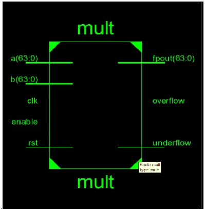
The high speed double precision floating point multiplier performs multiplication operation. The Black box view and the block diagram of high speed double precision floating point multiplier (mult) are shown in figures 2 and 3 respectively. It consists of seven sub operations i.e. sign bit calculation, exponent addition, placing the decimal point in the significant, multiplying the mantissa by using tiling technique, normalization, underflow/overflow and rounding. The input signals to the top level module are Clk, Rst, Enable, Opa (64 bits), and Opb (64 bits), where as the output signals are Fpout (output from operation, 64 bits), Underflow, and Overflow.
An 11-bit ripple carry adder is used to add the two input exponents. The black box view of adder module (adder1)
[image:2.595.109.507.570.739.2]is shown in Figure 4. .
Figure 2: Black box view of high speed double Precision floating pointmultiplier
Figure 3: Block diagram of high speed double precision floating point multiplier (mult).
Figure 4: Black box view of adder module
The mantissa of operand A and operand B, and the leading ‘1’ (for normalized numbers) are stored in the 53-bit registers (mul_a) and (mul_b) respectively. Multiplying all 53 bits of mul_a by 53 bits of mul_b would result in a 106-bit product. Depending on the synthesis tool used, this might be synthesized in different ways that would not take efficient advantage of the multiplier resources in the target device. 53 bit by 53 bit multipliers are not available in the most popular Xilinx and Altera FPGAs, so the multiply would be broken down into smaller multiplies and the results would be added together to give the final 106-bit product. Instead of relying on the synthesis tool to break down the multiply, which might result in a slow and inefficient layout of FPGA resources, the module (fpu_mul) breaks up the multiply into smaller 24-bit by 17-bit multiplies. The Xilinx Virtex6 Device contains DSP48E slices with 25 by 18 twos complement multipliers, which can perform a 24-bit by 17-bit unsigned multiply.
The products are added together, with the appropriate offsets based on which part of the A and B arrays they are multiplying. For example, product_b is offset by 17 bits from product_a when adding product_a and product_b together. Similar offsets are used for other product when adding them together. The summation of the products is accomplished by adding one product result to the previous product result instead of adding all products together in one summation. The goal is to take advantage of the adders in the Virtex6 DSP48E slices that follow each 24 by 17 multiply block.
4. FLOATING POINT
MULTIPLICATION ALGORITHM
The normalized floating point numbers have the form Z = (-1S) * 2 (E - Bias) * (1.M). To multiply two floating point numbers the following procedure is adopted. 1. Obtaining the sign; i.e. Sa xor Sb
2. Adding the exponents; i.e. (E1 + E2 – Bias) 3. Multiplying the significand; i.e. (1.M1*1.M2) 4. Placing the decimal point in the significant result 5. Normalizing the result; i.e. obtaining 1 at the MSB of the results significant
6. Rounding the result to fit in the available bits 7. Checking for underflow/overflow occurrence
Consider a floating point representation similar to the IEEE 754 double precision floating point format, but with a reduced number of mantissa bits to 8 (i.e. consider mantissa bits from 51 to 44, and the remaining bits treated as zeros) while still retaining the hidden ‘1’ bit for normalized numbers. The equations for multiplier and multiplicand are
A = (-1Sa) * 2 (Ea - Bias) * (1.Ma), B = (-1Sb) * 2 (Eb - Bias) * (1.Mb). The notation of multiplication AB is AB = [(-1Sa) * 2 (Ea - Bias) * (1.M
a)] * [(-1Sb) * 2 (Eb - Bias) * (1.Mb)].
This can be reduced to
AB = (-1Sa+Sb) 2 (Ea+Eb - Bias) (1.Ma *1.Mb).
5.
MULTIPLYING THE MANTISSA BY
USING TILING TECHNIQUE
The mantissa multiplier will be built using the tiling technique. Let us consider our multiplication operands A and B on p and q bits respectively. Multiplication of multiplier (A) and multiplicand (B) can be done by efficient use of the DSP blocks in FPGAs. The technique consists in tiling a p×q rectangular board using a minimal number of such multipliers. Starting from the tilled board, the circuit equation is obtained using a simple rewriting technique
[image:3.595.93.277.71.217.2](a) Xilinx (b) Tiling Technique
Tiling is a technique for efficient use of the DSP resources in Field Programmable Gate Array.
DSP blocks in the Xilinx core are shown in figure 5(a). Figure 5(b) shows the 24*17 Virtex-6 DSP48E signed multiplier. This supports rectangular tiles in order to optimize the use of multipliers and adders within the DSP blocks. Figure 5(b) shows the eight Virtex-6 multiplier tiles denoted by M0 to M8. Each multiplier tile performs the multiplication of the order 24×17 bits .
Each rectangle represents the product between a range of bits from A and B. i.e. M1 = a[23:0] × b[16:0], M2 = a[23:0] × b[33:17],M3 = a[16:0] × b[52:34], M4 = a[33:17] × b[52:34], M5 = a[52:34] × b[52:41], M6 = a[52:34] × b[40:24], M7 = a[52:41] × b[23:0], M8 = a[40:24] × b[23:0], and M0 = a[33:24] × b[33:24]. For each rectangle, A and B axis represents the number of bits of A and B respectively. A rectangle has a weighted contribution to the final product, the weight being equal to the sum of its upper right corner axis range. The tiling technique multiplication equation is
AB = 20+0 M1 + 20+17M2 + 20+34M3 + 217+34M4 +
234+41M5+234+24M6 + 241+0M7 +224+0M8 +224+24 M0. Rewriting the above equation as
AB = ( M1 + 2 17
M2 + 2 34
M3 + 2 51
M4 ) S0 + 224 (M8 + 217M7 + 234M6 + 251M5) S1
+ 248 M0 ………. (1) Multiply the each sub tile and get product length of all tiles as
M1 = a[23:0] × b[16:0] = 41 product bits M2 = 41 bits,
[image:4.595.331.541.145.291.2]M3 = 36 bits, M4 = 36 bits, M5 = 31 bits, M6 = 36 bits, M7 = 36 bits, M8 = 41 bits, and M0 = 20 bits.
Figure 6: Black box view of combinational multiplier module
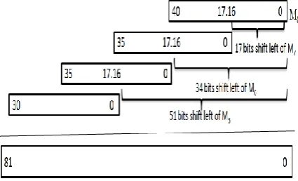
The black box view of combinational multiplier module is shown in Figure 6. M1, M2, M3 and M4 rectangles are added with each right shift of 17 bits and sum is stored in S0 register which is the length of 87 bits shown in figure 7(a).
Figure 7(a): Output of S0 register (Shift and Sum of M1,
M2, M3, M4 Multiplier tiles)
M8, M7, M6 and M5 rectangles are added with each right shift of 17 bits and sum is stored in S1 register which is the length of 82 bits shown in below figure 7(b). Finally S0 and S1 are added to M0 with the right shift of 24 bits which gives final output with a length of 106 bits as shown in figure 7(c).
Figure 7(b): Output of S1 register (Shift and Sum of M5, M6, M7, M8 Multiplier tiles)
Equation 1 is used to make full use of the Virtex-6 internal DSP adders. Due to the fixed 17-bit shifts between the operands, each sub-sum S0 and S1 may be computed entirely using DSP block resources. So in this algorithm the number of adders required for adding partial products are reduced to three (i.e. addition of S0, S1, M0).
6. UNDERFLOW/OVERFLOW
DETECTION
[image:4.595.85.279.395.733.2] [image:4.595.336.549.431.560.2]exponent addition may be compensated during subtraction of the bias, resulting in a normal output value (normal
operation). An underflow may occur while subtracting the
Figure 7(c): Final output (Shift and Sum of S0 and S1 registers, Multiplier tile M0)
bias to form the intermediate exponent. If the intermediate exponent < 0 then it’s an underflow that can never be compensated. If the intermediate exponent = 0 then it’s an underflow that may be compensated during normalization by adding 1 to it.
When an overflow occurs an overflow flag signal goes high and the result turns to ±Infinity (sign determined according to the sign of the floating point multiplier inputs). When an underflow occurs an underflow flag signal goes high and the result turns to ±Zero (sign determined according to the sign of the floating point multiplier inputs). Denormalized numbers are signaled to Zero with the appropriate sign calculated from the inputs and an underflow flag is raised. Assume that E1 and E2 are the exponents of the two numbers A and B respectively, the result’s exponent is calculated by using the equation
Eresult = E1 + E2 – 1023.
E1 and E2 can have the values from 1 to 2046, resulting in
Eresult having values from -1021 (2-1023) to 3069
(4092-1023), but for normalized numbers, Eresult can only have the values from 1 to 2046. Table 1 shows the E result for different values of exponent and the effect of normalization on it.
7. FLOW CHART OF HIGH SPEED
DOUBLE PRECESSION FLOATING
POINT MULTIPLIER
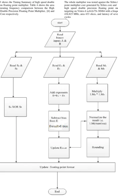
The flow chart of high speed double precession floating point multiplier is shown in figure 8.
Table 1: Normalization effect on Eresult’s exponent and overflow/underflow detection
Eresult Category Comments
-1021≤ Eresult <0
Underflow Can’t be compensated during normalization
Eresult =0 Zero May turn to normalized number during normalization (by adding 1 to it)
1≤ Eresult <2046 Normalized number
May result in overflow during normalization
2047≤ Eresult Overflow Can’t be compensated
8.
SIMULATION RESULTS
The high speed double precision floating point multiplier design based on tiling technique was simulated in Modelsim 6.6c and synthesized using Xilinx ISE 13.1i
Table 3 shows the Timing Summary of high speed double precision floating point multiplier. Table 4 shows the area and operating frequency comparison between the High Speed Double Precision Floating Point Multiplier,[6] and Xilinx Core respectively.
The whole multiplier was tested against the Xilinx floating point multiplier core generated by Xilinx core and [6].The high speed double precision floating point multiplier targeting on Virtex-6 xc6vlx75t-3ff484 with a frequency of 436.815 MHz, area 433 slices, and latency of seven clock cycles
.
Figure 9:Simulation results ofhigh speed double precision floating point multiplier
Table 2: Device utilization summery of high speed double precision floating point multiplier
Device utilization summary
Logic Utilization Used Available Utilization
Number of Slice Registers 433 93120 0%
Number of Slice LUTs 238 46560 0%
Number of fully used LUT-FF pairs 197 474 41%
Number of bonded IOBs 197 240 82%
Number of BUFG/BUFGCTRLs 1 32 3%
Number of DSP48E1s 9 288 3%
Table 3: Timing Summary of double precision floating point multiplier
Sl. No. Parameter Value
1 Minimum period (ns) 2.274
2 Maximum Frequency (MHz) 439.696
3 Minimum input arrival time before clock (ns) 0.947
Table 4: Area and Frequency Comparison between the High Speed Double Precision Floating Point Multiplier, [6] and Xilinx Core
Device parameters Present Work (Virtex-6) M.Al-Ashrafy,
A.Salem and W.Anis [6]
Xilinx Core
No. of slices 433 604 266
No. of Flip flops 197 293 241
Maximum Frequency (MHz) 436.815 301.114 221.484
9. CONCLUSION
The high speed double precision floating point multiplier supports the IEEE 754 binary interchange format, targeted on a Xilinx Virtex-6 xc6vlx75t-3ff484 FPGA. It achieves 436.815 MFLOPs which is 30.9% and 97% fast compared to [6] and Xilinx core respectively. This design occupies 433 slices which is 28% less compared to [6] and 38.6% more compared to Xilinx core. In terms of number of used flip flops, this design uses 197 flip flops i.e. 32.7% and 18% less compared to [6] and Xilinx core. This design handles the overflow, underflow, and truncation rounding mode.
10. REFERENCES
[1] B. Fagin and C. Renard, “Field Programmable Gate Arrays and Floating Point Arithmetic”, IEEE Transactions on VLSI, vol. 2, no. 3, pp. 365–367, 1994.
[2] N. Shirazi, A. Walters, and P.Athanas, “Quantitative Analysis of Floating Point Arithmetic on FPGA Based Custom Computing Machines”, Proc. of the IEEE Symposium on FPGAs for Custom Computing Machines (FCCM‟95), pp.155–162, 1995.
[3] L. Louca, T. A. Cook, and W.H. Johnson,“Implementation of IEEE Single Precision Floating Point Addition and Multiplication on FPGAs” , Proc. of the 83rd IEEE Symposium on FPGAs for Custom Computing Machines (FCCM‟96), pp. 107–116, 1996.
[4] B. Lee and N. Burgess, “Parameterisable Floating-point Operations on FPGA”, Conference Record of the Thirty-Sixth Asilomar Conference on Signals, Systems, and Computers, 2002
[5] Sebastian Banescu,Florent de Dinechin, Bogdan Pasca “Multipliers for Floating-point Double Precision and Beyond on FPGAs”, Proc. of First International Workshop on Highly Efficient Accelerators and Reconfigurable Technologies (HEART2010),Tsukuba, Ibaraki, Japan, June 1, 2010.
[6] M.Al-Ashrafy, A.Salem and W.Anis, “An Efficient Implementation of Floating Point Multiplier”, Proc. of Electronics Communications and Photonics Conference (SIECPC) 2011, Saudi International, pp.1-5, 2011.
AUTHORS PROFILE
Addanki Purna Ramesh has more than 14 years of experience in teaching. He is presently working as Associate professor of Electronics and Communication Engineering at Sri Vasavi Engineering College, Tadepalligudem. He is Life Member of MIETE, Associate Member in Institute of Engineers (India).
A. V. N Tilak has more than 25 years of teaching and research experience. He obtained his Master’s degree from Indian Institute of Technology, Kanpur and Ph.D. from Indian Institute of Technology, Madras during 1984 and 1997 respectively. He is presently working as a professor of Electronics and Communication Engineering at V.R.Siddhartha Engineering College, Vijayawada. He is Member of IEEE, Fellow of Institution of Electronics and Communication Engineers (IETE), Fellow of Institute of Engineers (India). He is also life member of Indian Society for Technical Education (ISTE).


![Table 4: Area and Frequency Comparison between the High Speed Double Precision Floating Point Multiplier, [6] and Xilinx Core](https://thumb-us.123doks.com/thumbv2/123dok_us/8097983.786770/9.595.119.500.97.243/table-frequency-comparison-double-precision-floating-multiplier-xilinx.webp)
