DIGITAL EQUIPMENT CORPORATION, Corporate Headquarters: Maynard, Massachusetts 01754, Telephone: (617) 897-5111
SALES AND SERVICE OFFICES
DOMESTIC - ARIZONA, Phoenix and Tucson. CALIFORNIA, Los Angeles, Monrovia, Oakland, Ridgecrest, San Diego, San Francisco (Mountain View), Santa Ana, Sunnyvale and Woodland Hills. COLORADO, Englewood. CONNECTICUT, Fairfield and Meriden • DISTRICT OF COLUMBIA, Washington (Latham, Md.) • FLORIDA, Orlando. GEORGIA, Atlanta. ILLINOIS, Chicago (Rotling Meadows) • INDIANA, Indianapolis. IOWA, Bettendorf. KENTUCKY, Louisville. LOUISIANA, Metairie (New Orleans) • MASSACHUSETTS, Marlborough and Waltham. MICHIGAN, Detroit (Farmington Hills) • MINNESOTA, Minneapolis. MISSOURI, Kansas City and St. Louis. NEW HAMPSHIRE, Manchester. NEW JERSEY, Fairfield, Metuchen and Princeton. NEW MEXICO, Albuquerque. NEW YORK, Albany, Huntington Station, Manhattan, Rochester and Syracuse. NORTH CAROLINA, Durham/Chapet Hill • OHIO, Cleveland, Cotumbus and Dayton. OKLAHOMA, Tulsa. OREGON, Portland. PENNSYLVANIA, Philadelphia (Bluebell) and Pittsburgh. TENNESSEE, Knoxville. TEXAS, Austin, Dallas and Houston • UTAH, Salt LakeCity. WASHINGTON, Bellevue. WISCONSIN, Milwaukee (Brookfield) • INTERNATIONAL - ARGENTINA, Buenos Aires. AUSTRALIA, Adelaide, Brisbane, Canberra, Melbourne, Perth and Sydney. AUSTRIA, Vienna. BELGIUM, Brussels • BOLIVIA, La Paz. BRAZIL, Puerto Alegre, Rio de Janeiro and Sao Paulo. CANADA, Calgary, Halifax, Montreal, Ottawa, Toronto and Vancouver. CHILE, Santiago • DENMARK, Copenhagen. FINLAND, Helsinki. FRANCE, Grenoble and Paris • GERMANY, Berlin, Cologne, Hannover, Hamburg, Frankfurt, Munich and Stuttgart • HONG KONG • INDIA, Bombay • INDONESIA, Djakarta • ISRAEL, Tel Aviv • ITALY, Milan and Turin. JAPAN, Osaka and Tokyo • MALAYSIA, Kuala Lumpur. MEXICO, Mexico City. NETHERLANDS, Utrecht. NEW
GENERAl INfORIIATIOII
GENERAL PUJIPOSE MODULES
Full ra . . of
cficitaI
and ...ICJIic
1M °1« . . . _I/O interf
COMPUTER IN1'EJWACINS MODULES
far DEC POP", PDP· 1 1, PDP·12, PDP-15
DECkits
Complete 1/0 Interfaces in kit form
MICROPROCESSORS
Computers on a board
REGISTER TRANSFER MODULES
Designing logic systems utilizing Regtster Transfer concepts
TERMINALS
Remote, ASCII, data acquisition/ entry termina's
HARDWARE/CABLESI POWER SUPPLIES
Cabinets, connectors, and, similar assembly items
LAB SERIES
Basic and advanced logic design aids
;"~'~
handbook
1975-76
prepared
by
logic products group
Copyright
©
1975 by Digital Equipment CorporationDigital Equipment Corporation makes no representa-tion that the interconnecrepresenta-tion of its modular circuits in the manner described herein will not infringe on existing or future patent rights. Nor do the descrip-tions contained herein imply the granting of licenses to make, use, or sell equipment constructed in accord-ance herewith.
Digital Equipment CorporaUon is not responsible for errors which may appear in the pricing, technical descriptions, illustrations, or photographs of the products appearing in this Handbook.
Digital Equipment Corporation reserves the right to make substitutions a.nd modifications in the specifica-tions of the products described in this Handbook_
Prices quoted are in U.S. dollars and apply
to
the United States only. The availability of products listed and the prices quoted herein are subject to changewithout notice. .
FLIP CHIP, UNIBUS and OMNIBUS are trademarks of Digital Equipment Corporation,
FOREWORD ... !\,... ix
INTRODUCTION ... , ... , ... ,... xi
GENERAL INFORMATION ... ,... 1
Special Symbols and Abbreviations ... 1
Module Contact Finger and Module Connector Block Contact Identification ... 6
Module Dimensions ... .... 10
Related Literature ... ... 11
Module Cleaning ... ... 11
GENERAL PURPOSE LOGIC AND CONTROL MODULES ... 13
M SERIES ... ... 16
General Characteristics ... ... 16
Operating Characteristics .. ... 19
Gates ... ... 34
Flip·Flops and Registers . ... 54
Time·Related .. ... ... ... 76
Numeric ... ... 94
Logic Amplifiers ... :... .. ... 121
Miscellaneous... ... 129
A SERIES ... ... 158
Notes on Operational Amplifiers ... ... 15S' A Series Analog Modules ... 167
K SERIES ... . ... 193
General Characteristics ... 193
K Series Control Modules ... 197
MODULES NOT RECOMMENDED FOR NEW DESIGN ... 260
M Series ... , ... > ••••••••••••••••••••••• 260 B Series ... 261
R Series ... 263
W Series ... 266
COMPUTER INTERFACING MODULES ... 271
PDP·8 FAMILY ... 272
OMNIBUS Interfacing Principles ... , ... 272
External Bus Operation... ... 275
OMNIBUS·Related Interface Modules ... 277
NON·OMNIBUS Interfacing ... ... .. ... 294
Positive Bus Modules... ... 294
Negative Bus ·Modules ... ... 333
PDp·ll FAMILy ... ... 351
UNIBUS Interfacing Principles ... 351
PDp·ll UNIBUS Interface Modules ... 354
PDP·12 INTERFACING ... ... .. ... 401
DECKITS ... 409 General Description ... ... .... . .... 410 DECKit11-H PDP-ll I/O Interface (4 Words In/4 Words Out) ... 411 DECKit11-F PDP-ll 110 Interface (3 Words In/1 Word Out) .... 413 DECKit11-K PDP-ll I/O Interface (8 Words In) . . . '" ... 414 DECKit11-M PDP-ll I/O Interface (34 Bits In/24 Bits Out. 418 DECKit11-D PDP-ll Direct Memory Access Interface ... . 421 DECKitOl-A Remote Analog Data Concentrator.. . ... 424 MICROPROCESSORS ... . ... 431
Introduction .. .... 432
Microprocessor Series (MPS) Modules 432
Operator's Control Panel, KC341-B .. '" 446
Read-Only Memory Programmer, MR873-A ... ... . ... 448 Prewired Backplane, KMPOI-A .. '. . ... 450
Software" Tools ... . ... 452
REGISTER TRANSFER MODULES (RTM) ... . General Description ....
Register Transfer Modules
DATA ENTRY TERMINALS ... , .... . PDM70 Programmable Data Mover . RTOI Data Entry Terminal.
RT02-A Alphanumeric Data Entry Terminal. RT02-B Full Keyboard Alphanumeric Terminal RT02-C Badge Reader Terminal ..
Custom Terminal Capabilities
VT50 DECscope Video Display Terminal LA36 DECwriter II Data Terminal
HARDWARE/CABLE ASSEMBLIES/POWER SUPPLIES HARDWARE ... .
Cabinets and Cabinet Accessories. 19-1nch Electronics ~ack Mounting Panels Four-Slot System Units
Nine-Slot System Units ... Module System Enclosures ... . PDP-8/E Expansion Hardware .. Module Connector Blocks Cable Connectors ... . Cable Clamps .: .... .
Blank Module Boards ...
Wire Wrappable Module Boards .
Collage Module Boards.. . ... . Special Purpose Blank Module Boards
. ... 455 . ... 456 457 545 546 552 554 556 558 560 561 564 569 ... 572 572
584-587 589 . .... 590 . ... 595 ... 595 597 609 610 613 ... 615 ... &16 Module· Extender Boards
Integrated Circuit Sockets .
... 616 . ... 618
Integrated Circuits ... 618
Module Handles, Module Handle Extenders, and Module Holders.
Wire Wrapping Tools and Accessories ... . Bus Strips
Patch Cords and Accessories . . ... .
Wire ... . ... .
CABLE ASSEMBLIES . . . .. . ... . ... . POWER SUPPLIES, POWER CONTROLLERS, AND POWER SUPPLY ACCESSORIES ... ... . ... .
LAB SERIES ... ... 639
Computer Lab ... ... 641
DEClab-RT ... 643
ABOUT DIGITAL EQUIPMENT CORPORATION ... 645
GENERAL DESCRIPTION OF DIGITAL PRODUCTS ... .. DIGITAL ENGINEERING SERViCES ... . 647 649 TERMS AND CONDITIONS ... 650
INDEX ... 653
viii
This tenth edition of the lOGIC HANDBOOK is your guide to the most exten-sive line of products ofrenMI by Di(ptal fqpipe at Corporation for
implement-ing etectronic logic designs for iHSttu,iientalWn, computer iMerfacin& data gathering or control. This handbook is a basic reference for anyone involYecf
in specifyi"... manufacturing or using solid·state logic.
Our M Series TTL-integrated circuit modules are featured throughout this edition. The M Series line consists of more than 100 modules ranging from basic and fundamental logic modules to self-contained computer interfacing modules. The impact of advancing technology can be seen in M Series evolu-tion. From the beginning, M Series was TIL integrated cirCUit-oriented; the current trend is toward MSI and LSI. The result is more complexity (and more built·in design solutions) per module. Many of the modules in this handbook amount to full-scale digital subsystems.
The microprocessor or "computer-on·a-chip" is the latest result of the con-tinuing technological advancements. As the leading supplier of logic modules, DIGITAL applied this microprocessor concept to a family of modules desig-nated Microprocessor Series (MPS). The major CPU functions are executed by
a
single-chip, MOS/LSI microprocessor. All input and output lines are TIL levels, thus making the MPS compatible with other M Series modules. Further versatility has been added to the M Series line by the availability of six prewired Interfacing Kits, described herein. Five of the kits offer the user the capability of implementing more complex input/output interfacing be· tween a PDP-II computer and peripheral equipment at- low cost and mini-mum design time. The sixth kit provides a convenient method of monitoring analog voltages at a remote location.An alternative logic design concept has been made available to the designer of digital systems with the availability of RT Modules described in this hand-book. These modules, using the Register Transfer concept, minimize design time, reduce documentation, and demand only a fundamental knowledge from the system designer.
This edition of the handbook also covers the K Series of industrial control modules, the A Series of analog modules, the W Series of wire wrappable modules, collage and blank boards in the FLIP CHIP form factor, and a com-plete line of power supplies, hardware, and cables. All these support support functions provide a total capability for designing, implementing, and assem-bling a modular system, small or large, at the lowest cost per function in the industry.
Extensive noncatalog products and services are also available from DIGITAl. If you require unique functions that are not listed in this handbook, contact your local DIGITAL office. The product you need may be available as a non-catalog item. In addition, DIGITAL maintains a Special Module Products Group with complete capability of module design, layout, manufacturing and test. Custom product capability is not limited to modules alone but extends to the support hardware and accessories, including cabling, wire wrapping, and cabinets.
A worldwide staff of DIGITAL sales engineers is prepared to respond to your technical and commercial needs. From a backlog of logic system design
ex-perience, DIGITAL may have a detailed solution to your application or inter-face requirement.
Please address any comments on this handbook, or inquiries concerning special services, to:
x
Digital Equipment Corporation Components Group
One Iron Way
Marlborough, Massachusetts 01752
Attn: Logic Products
Sales Support Manager
ORGANIZATION OF HANDBOOK
This edition of the LOGIC HANDBOOK is organized into eight functional sec-tions for maximum ease of reference. Within each section, module descrip-tions are arranged by categories acco·rding to funcdescrip-tions. To locate a specific item, consult the Product List at the end of the handbook.
General Purpose Logic and Control: This section includes all of the M Series, A Series, and K Series basic logic modules and those complex functional modules that are not specifically computer-interface oriented. In addition, brief descriptions are provided of earlier modules that are still valid for spares and replacements.
Computer Interfacing: This group includes the M Series complex functional modules that simplify interfacing to the PDP-l1 UNIBUS, PDP-8/A, 8/E, 8/F, 8/M OMNIBUS, PDP-12, and PDP-15. Also in this group are the modules for interfacing the external I/O bus of earlier PDP-8 family computers plus level converters and other interface·oriented support modules. Introductory in-formation defines the control and data signals of the OMNIBUS, UNIBUS, and external. I/O bus.
DECkits: These kits offer greater interfacing capability to the PDP-ll UNIBUS at the lowest cost possible. Complex logic module building block concepts are now expanded to greater limits of versatility in kit form. Capable of per-forming a highly complex computer interface, the kit is a collection of logic modules inserted by the user to a prewired system unit.
Microprocessors: Employing state-of-the·art semiconductor technology, DlGI· TAL's Microprocessor Series consists of a processor module, a read/write memory module, a programmable read-only memory module, and an external event detection module. Other support features, such as an operator's con-trol panel and software routines, are also described in this section.
Register Transfer Modules: Register Transfer (RT) defines the next higher level of computing machine design above sequential and combinatorial logic operations. Digital system design is removed from the realm of the pure logic designer and is made easily achievable by persons such as students, laboratory technicians, researchers, etcs.
RT modules can be operated in 8-bit or 16-bit register configurations; regis-ters may be linked to form words of 24, 32, or higher numbers of bits. The modules are especially useful at the university teaching level, in experi-mental, medical, and research laboratories, industrial control, materials handling, and manufacturing.
The terminals feature Teletype and EIA serial line compatibility. Interface to a computer is accomplished via a standard full-duplex 4-wire data communi-cations Teletype interface. Standard interfaces are available for the PDP-S, -10, -II, -12, -15, and -16 computers. Modem interface signals corresponding to EIA RS-232C specifications are also provided.
Cables, Power Supplies, Hardware: This section describes a wide selection of prefabricated cables for interconnection of free-standing logic systems as well as computer-based installations. Bulk cables and cable cards are avail-able so that the user can design and "Construct his own custom intercon-nections with a minimum of custom design and planning.
A wide selection of dc power supplies for small and large,systems is provided here.
DIGITAL makes a complete line of hardware accessories to support its mod-ule series. Modmod-ule connectors are available for as few as one modmod-ule to as many as 64 in a single 19" mounting panel. A complete line of cabinets is available to house the modules and their connector blocks, as well as provide a convenient means for ·system expansion. Wiring accessories and a com-plete selection of support hardware simplify all phases of physical construc-tion. This edition's hardware selection is expanded to include the latest cabinet and hardware features.
SPECIAL SYMBOLS AND ABBREVIATIONS
Logic symbols used in this handbook conform, in general" to widely accepted MIL standards. All basic M Series logic symbols (AND, OR, NAND, NOR, Inverter, Flip-Flop) are described in the introduction to the M Series logic and control modules.
Input Loading and Output Drive
On the logic diagrams of this handbook, input and output loading, expressed in TTL unit loads, appear in boxes terminating each input or output signal line. In the 2-input NAND gate example of Figure I, both inputs (pins Al and B1) present one TTL unit load. The output (pin CI) is capable of driving 10 TTL unit Idads. The arrows eliminate any possible confusion as to the direction of signal flow.
INPUT LOAOING PIN NUMBER (I TTL UNIT LOAOY(PIN A, SlOE II
1 AI
ARROWS SHOW DIRECTION OF SIGNAL FLOW
Figure 1. Logic Diagram Input Loading and Output Drive Symbols
Bus Drivers and Receivers
DATA TO BUS
B U2
DRIVE TO BUS
~B1 •
_ _ _
--.,~eus
DRIVERREAD FROM BUS
DATA FROM
BUS
TYPICAL BUS TRANSCEIVER ARRANGEMENT
Figure 2. Bus Driver and Receiver Symbols
Electrical characteristics of these circuits are described in the introduction to M Series Computer Interfacing Modules.
level Converters
Whenever logic levels are translated from one set of voltages to another, the conversion is shown taking place in a square level-converter symbol. Inside the box, the corresponding logic levels are related in a simple truth table. The example of Figure 3 shows a level converter stage that accepts TTL levels (LOW and HIGH) and delivers DEC negative voltage levels (-3 V and ground).
Input loading is two TTL unit loads. Whenever loadtng is peculi.ar, it is de-fined in a note on the drawing as in the output of Figure 3.
~_JH4
__ ._
D1Q~
*=SINKS 20mA AT GROUNDSpecial Analog Symbols
Symbols used on analog circuit drawings to represent multiplex switches and , operational amplifiers are shown in Figure 4. Loading boxes for analog inputs and outputs contain the letter "A"; do not connect such sign,als to logic levels.
MJlTIPLEX SWITCH (MOS FETl CONSTANT IMPEDANCE MULTIPLEX SWITCH
~
ALOGIC CONTROL·
INPUT
LOGIC
CONTROL---' INPUT
_1t>~1
OPERATIONAL AMPLIFIER
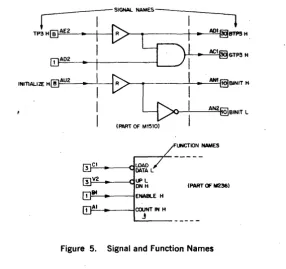
Signal and Function-Names
Inputs and outputs of M Series IOSic modules may be assigned a signal name, a function name, or both. (See Figure 5.) Signal names appear
out-side blocks or logic symbols to identify typical input or output signals.
_ _ - - - S I G N A L NAMES--_ _ _ _ _ _
r
I
I
1
~H:::
:
!
G>
L[)~!:
::::
r=::..-..---'-I--I
I •
ANt~8INIT
HI
I
I
X>--.l...-I
---==t1I
(PM"T OF Mt510)I
t=---c::::J~f L
~ _ _ ~(]UPL
DNH 1="-___ -~ENABl.E H
~ ___ ---IcaJNT IN H
j
(PART OF M2M1
Figure 5. Signal and Function Names
Digital Equipment Corporation uses standard terminology to name signal lines to aid the reader in determining their active state. Either an H or L follows the Signal name mnemonic, separated by a space. This letter indi-cates the asserted. (true) state of the signal. An H means the signal is as-serted when HIGH (+3 V) and an L means the signal is asas-serted when LOW (0 V). For example, a UNIBUS data line is called BUS 000 L and a grant line is called BUS BG4 H.
On the logic diagrams of many computer interfacing modules in this hand-book, signal names peculiar to one computer, such as the PDP-II, appear as an example of typical usage. Signal names may be changed to those of another computer or interfacing device if logically appropriate.
Function names appear inside the blocks of functional modules. They iden-tity the function of input or output Signals. The user may add his own signal names. .
Abbreviations
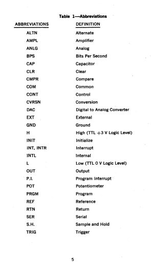
Abbreviations used in signal and function names in this handboo~. are de-fined in Table 1.
[image:18.380.54.340.89.358.2]ABBREVIATIONS
AlTN
AMPl
ANlG
BPS
CAP
ClR CMPR COM
CONT CVRSN
DAC EXT
GND H
INIT INT,INTR
INTL
l OUT . P.I.
POT
PRGM
REF RTN
SER S.H ..
TRIG
Table I-Abbreviations
DEFINITION
Alternate
Amplifier
Analog
Bits Per Second
Capacitor
Clear Compare Common
Control Conversion
Digital to Analog Converter
External
Ground
High (TTL +3 V logic level)
Initialize Interrupt
Internal
low (TTL 0 V logic level)
Output
Program Interrupt· Potentiometer
Program
Reference Return Serial
Sample and Hold
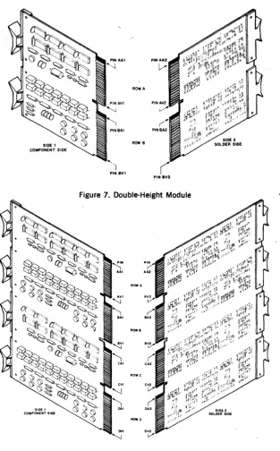
[image:19.378.49.344.41.557.2]MODULE CONTACT FINGER AND MODULE CONNECTOR BLOCI( CONTACT IDENTIFICATION
DIGITAL plug-in (FLIP CHIP) modules have contact fingers either on one side (single-sided modules) or on both sides (double-sided modules). Mod· ules with contact fingers on only one side always have them on side 2 (the solder side) (Figures 6, 7, and 8). DIGITAL module connector blocks have module slots with contacts either on one or on both sides. Modules with contact fingers on only one side can be plugged into connector blocks with contacts on both sides of the module slots; then electrical contact between the module and the connector block is only via module slot side 2 contacts. The module contact fingers and connector block contacts are identified by alphanumeric codes. These alphanumeric codes are used throughout this handbook, the HARDWARE ACCESSORIES CATALOG, the PERIPHERALS HANDBOOK, individual module data sheets, engineering drawings, and other DIGITAL publications. This coded numbering scheme must be understood to ensure proper system interconnections (Figures 6, 7, and 8). Letters G, I,
0, and Q are not used in this numbering scheme.
DIGITAL modules are SINGLE·HEIGHT, DOUBLE-HEIGHT, or QUAD·HEIGHT; STANDARD LENGTH or EXTENDED LENGTH; and SINGLE·WIDTH or DOUBLE· WIDTH (Figures 6, 7, and 8). Each DIGITAL module is a specific, fixed size; the size of each module is stated in the module description in the previously mentioned DIGITAL publications. DIGITAL SINGLE·HEIGHT and DOUBLE· HEIGHT modules are STANDARD LENGTH or EXTENDED LENGTH. DIGITAL QUAD·HEIGHT modules are always EXTENDED LENGTH. Any DIGITAL module can be SINGLE·WIDTH or DOUBLE-WIDTH; most, however, are SINGLE· WIDTH.
The height and length requirement is determined by the quantity and size of discrete components and integrated circuits located on side 1 of the module, and, to some extent, by the amount of etched printed circuitry on sides 1 and 2. The width requirement is determined by the distance the largest component extends from its mounting surface on the module.
Some DIGITAL module connector blocks accommodate only SINGLE-HEIGHT modules and others accept either SINGLE-HEIGHT or DOUBLE-HEIGHT mod-ules_ No single connector block can accommodate QUAD-HEIGHT modules; QUAD-HEIGHT modules must be mounted in mounting frames, system units, or module drawers comprising module connector blocks with slotted ends so that four module slots are arranged end to end (Le., at least two H863 or H8030 Module Connector Blocks mounted end to end). SINGLE-HEIGHT modules are 2.417/2.452 in. (6.139/6.228 cm) high, DOUBL.:E-HEIGHT modules are 5.167/5.202 in. (13.124/13.213 em) high, and QUAD-HEIGHT modules are 10.437/10.472 in. (26.510/26.599 cm) high (Figure 9).
SINGLE-HEIGHT modules (standard length and extended length) may be plugged into the upper (row A, C, or E) or lower (row B. 0, or F) module slot of a connector block (Figure 9). Contact fingers Al through VI are on side 1 (component side) of the module, and contact fingers A2 through V2 are on side (solder side) of the module (Figure 6).
DOUBLE-HEIGHT modules (standard length and extended length) have two plug-in sections of contact fingers and occupy two module slots (rows A and B, C and 0, or E and F) of a connector block (Figure 9). The two plug-in sections are identified by the designations A and B. Contact fingers Al through VI and A2 through V2 of the A section are designated AAI through AVI and AA2 through AV2, respectively; contact fingers Al through VI and A2 through V2 of the B section are designated BAI through BVl and BA2 through BV2, respectively (Figure 7). Note that the positioning notch in the module base must mate with the protrusion on the connector block for correct positioning.
QUAD-HEIGHT modules (always extended length) have four plug-in sections of contact fingers and occupy four module slots (rows A through 0 or C through F) of two connector blocks (Figure 9). The four plug-in sections are identified by the designations A, B, C, and D. The four sections of contact fingers are deSignated AAl through AVl and AA2 through AV2; BAl through BV1 and BA2 through BV2; CAl through CVl and CA2 through CV2; and DA1 through DV1 and DA2 through DV2 (Figure 8).
SIDE I COMPONENT SIDE
AI
PIN VI
PIN V2
ROW A
ROW B
' I
PIN BV1
PIN 8V2
. ht Module
7 Double-Helg Figure .
ROWB
ROW C
ROW 0
0112 0111 V '--.J
. ht Module
Quad-Helg
[image:22.380.29.342.25.529.2]ROW A
SINGLE - HEIGHT STANDARD-LENGTH MODULE
DOUBLE - HEIGHT EXTENDED-LENGTH MODULE
ROW BROW CROW 0
QUAD-HEIGHT EXTENDED-LENTH MODULE
ROW E ROW F
...,
QQ' c: CD....
p
3: 0I-' a.
0 c: CD
0 8.4~t .• 10
3'
(EXT. LGTH.l(I) ~ en 2;--~ en t:~:t
,. 10.4S~= .1
(QUAO. MGT.I
I. 8.000
,. !!.Z50 I .,
+
;1
r
7.438 ..
(EXT.lGTH.l
-1
II, (~~l~r--I :
4.930t .0I0
(STD.LGTH.l I
t',~:
2.750
1O.31Z .. (QUAD. HGT.)
--4
I
3.938<0
Il'
(STD. LGTH.I ,
.180TYP . .
NOtES:
DIMENSIONS DENOTED BY .. ARE FOR MAX. USEAI!I.£ CIACUIT AREA.
~ESS OTHERWISE SPEQAED ALL DIMENSIONS ARE t.OO& .
. IZ8 DIC:~ HANDLE HOLES
IIOntN Of FING£RS
TO TOP OF HANDLE 8.9<lt .• ,. (EXT. LGTH\
5.!IO t.o •• (STD. LGTH)
Il
: I
I :
I
I
1
II~J
-~
1
CCM>ONENT ~-.834 LIoIIT:4
_ - A nMAX_ .063
RELATED LITERATURE
Listed below ..Ire DIGITAL doc·uments that supplement the material provided in this handbook. These documents are available from the nearest DEC Sales Office.
• HARDWARE/ACCESSORIES CATALOG • PDP-ll PERIPHERALS HANDBOOK
• PDP-8/E, 8/F, 8/M SMALL COMPUTER HANDBOOK
MODULE CLEANING
Occasionally, modules which have been in service for a long period of time may develop resistive coatings on their gold-plated fingers. This coating, if allowed to build up, can cause malfunctions by decreasing the noise margin of a circuit.
There are two types of foreign material coatings which can develop on the gold-plated fingers ofa module. The first type is INORGANIC. This type of contamination results when copper "bleeds" through the gold plating and oxidizes. This oxidized layer builds up and can create contact resistances of significant consequence. Inorganic contamination is strictly a matter of time; however, extremely dirty environments will speed up the process. For this reason, care should be taken to locate modules and systems in an area as free from smoke, pollution, and other air·bound particles as possible. The second form of contamination involves ORGANIC substances, which usually are a result of careless handling, and are mainly made up of finger-prints, salts, and oils deposited when the modules are handled by the gold-plated fingers. Contamination by organic substances can be greatly reduced by careful handling of the modules.
Although the backplane connectors are 'of the self-cleaning type, it may be-come necessary to clean the module fingers to ensure reliable connection. When it has been determined that the module fingers are in need of cleaning, the following procedure is recommended.
Inorganic Contaminants
Immerse the fingers of the module in an ultrasonic bath of deionized water and a detergent, such as Liguinyx, for at least 30 seconds. Repeat with pure deionized water only.
It is now necessary to remove the water from the module fingers. This should be done immediately following the ultrasonic rinse since water wUl damage the module fingers if allowed to remain. The water can be removed by im~ mersing the module fingers in an ethand or methanol bath to the same depth used during the ultrasonic cleaning. Never wipe or use an abrasive cleaner on the module fingers. If wiping is necessary, the use of K-Dry is recommended.
Organic Contaminants
After inorganic contaminants and water have been removed, organic materi-als may be removed by immersion of the module fingers in trichloroethane for at least 30 \Seconds. The fingers can then be allowed to dry or may be
logic and
GENERAL PURPOSE
LOGIC AND
CONTROL MODULES
This section describes the computer industry's most extensive line of general purpose logic modules-modules used in DIGITAL's products and modules used by thousands of customers for computer interfacing, instrumentation, data gathering, and control. The module descriptions are organized into three main subsections: M Series, A Series, and K Series. In addition, a fourth subsection briefly describes earlier versions of selected M, W, R, and 8 Series modules.
M Series high-speed monolithic integrated circuit logic modules employ TIL (transistor·transistor logic) circuits which provide high speed, high fanout, large capacitance drive capability, and excellent noise margins.
The M Series includes a full digital system complement of basic modules which are designed with sufficient margin for reliable system operation at frequencies up to 6 mHz. Specific modules may be operated at frequencies up to 10 mHz. The integrated circuits are dual in-line packages.
In addition to the reduced cost of integrated circuits, DIGITAL's advanced manufacturing methods and computer-controlled module testing have re-sulted in considerable production cost savings, reflected in the low price of all M Series modules.
M Series modules are compatible with DIGITAL's K Series and, through the use of level converters, are compatible with all of DIGITAL's standard nega-tive-voltage FLIP CHIP modules.
A Series analog modules support the M Series by providing a two-way trans-lation between continually varying real-world voltage measurements and the digital realm of control and computation. The A Series emphasizes 10- and 12-bit performance in a family of mutually compatible functions-multiplex-ers, operational amplififunctions-multiplex-ers, sample-and-hold circuits, D/A and A/D convertfunctions-multiplex-ers, reference voltage sources, and an expanded group of multiplying D/A con-verters.
K Series modules have been specially designed for the industrial environment to replace mechanical relay logic. They are extreme.ly noise-immune and reli-able, allowing optimum combinations of solid-state logic to be applied to industrial control applications.
The upper frequency range of the K Series modules is 100 kHz, with provi-sion for reduction to 5 kHz for maximum noise immunity. These modules incorporate all-silicon diodes, tranSistors, and integrated circuits, deliberately slowed through the use of discrete components.
Either English (noninverting) logic or NAND/NOR logic is compatible with K Series. The hardware for this series is specifically designed for standard NEMA enclosures. FLIP CHIP mounting hardware can likewise be used for rack-mounting, since K Series modules fit standard FLIP CHIP module con-nectors.
M SERIES
GENERAL CHARACTERISTICS
M Series high-speed, monolithic integrated circuit logic modules employ TIL (transistor-transistor logic) integrated circuits which provide high speed, high fan out, large capacitance drive capability and excellent noise margins. The M Series includes a full digital system complement of basic modules which are designed with sufficient margin for reliable system operation at frequencies up to 6 MHz:. Specific modules may be operated at frequencies up to 10 MHz. The integrated circuits are dual in-line packages.
The M Series printed circuit boards are identical in size to the standard FLIP CHIPTM modules. The printed circuit board material is double-sided pro-viding 36-pins in a single height module. Mounting panels (H910 and H911) and 36-pin sockets (HS03 and HSOS) are available for use with M Series modules. Additional information concernin"g applicable hardware may be found in the Power Supply & Hardware and Accessories section of this handbook.
M Series modules are compatible with Digital's K Series and, through the use of level converters, are compatible with all of Digital's other standard negative voltage logic FLIP CHIP(i) modules.
TTL NAND GATE
The basic gate of the M Series is a TIL NAND GATE. Figure 1 is the basic two input NAND gate schematic diagram. The circuit is divided into 3 major sections, the multiple emitter input, the phase splitter and the totem pole output circuit. The two diode model of a transistor shown in Figure 2 will be used in the analysis of the circuit. A forward biased silicon junction (i.e. diode) gives a voltage drop of about 0.75 volts and a saturated silicon transistor has a collector emitter voltage of 0.4 volts average. These two figures will be used throughout the following discussion.
With either input at the LO logic level (O.OV-O.SV) the multiple emitter input transistor will be ON with its base residing at about 0.75
+
0.4 = 1.15 volts. The three diode string consisting of QI'S base collector diode, Q2'S base emit-ter diode, and Q/s base emitemit-ter diode will have only 1.15 volts across it and will therefore be conducting only leakage currents (0.75+
0.75+
0.75=
2.25 volts required for forward bias). With no current flowing into the base emitter junction of Q2, the transistor will be OFF and its collector emitter voltage is alowed to rise. Similarly with no current flowing in the base emitter diode of Q. the transistor is OFF and its collector emitter voltage is allowed to "rise. When both Q2 and Q4 are OFF, QJ is freed to pull the output voltage to a HI level. The voltage levels present in the circuit with one or more LO in-puts is shown in Figure 4. I~---.---e---+ev
41( 1.61( llOA
03
•
INPUT A ---"..L.._..-.~---H 02
~---~
INPUT 8 - - - -...
Q4
IK
___ __.._---J
'---'~______
----MULTIPLE EMITTER
INPUT
PHASE SPLITTER
TOTEM
POLE
OUTPUT
Figure 1 TTL NAND Gate Schematic Diagram
COLLECTOR
BASE BASE
EMITTER
Figure 2 Two Diode Model For Transistor
CURRENT
PATH
r
-+sv
Q2BE Q4BE
INPUT A ---!-iO---=-===-f----C>....-T--ot---C>t---, I
INPUT B (LOW)
L _________
I ...1 [image:31.379.32.354.17.553.2]INPUT A HIGH
INPUT B
LOWIO.4VI
..
4K
MULTIPLE EMITTER
INPUT
+5V
f.6K ,30A
03
l.5V
OUTPUT
04
~---4---G~
TOTEM POLE OUTPUT
Figure 4 TIL NAND Gate Schematic Diagram, One Input LO
4K
l~T
INPUT A --"H;:.:IG::..:.H-t_----+Z:=Z::::5:::::V~ot_----*--_coI--....,
INPUT 8 ---'-'.";.:;'GH'-'---+o-_ _ -J
Figure 5 Diode Equivalent NAND Gate Circuit, Both Inputs HI
INPUT A HIGH 12.4VI
INPUT B HIGHIZ.4VI
4K
Z.Z5V
MULTIPLE EMITTER
INPUT
1.6K
t t5V
QZ i04V
tK
PHASE SPLITTER
O~V
1lOA
TOTEM
POLE
OUTPUT
03
04
+5V
04V
OUTPUT
GIIOJNO
OPERATING CHARACTERISTICS
Power Supply Voltage: 5 Volts ± 5% Operating Temperature Range: 0° to 700e
Speed: M Series integrated circuit modules are rated for operation in a sys-tem environment at frequencies up to 6 MHz. Specific modules may be oper-ated at higher frequencies as indicoper-ated by the individual module specifica-tions.
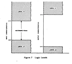
LOGIC LEVELS AND NOISE MARGIN
A gate input will recognize 0.0 volts to 0.8 volts as logical LO and 2.0 volts to 3.6 volts will be recognized as a logical HI. An output is between 0.0 volts and 0.4 volts in the logical LO condition. The logical HI output condition is between 2.4 volts and 3.6 volts. Figure 7 shows diagrammatically the accept· able transistor-transistor logic levels. The worst case noise margin is 400 millivolts that is, an output would have to make at least a 400 millivolt excur-sion to cause an input which is connected to it to go into the indetermined voltage region. For instance if an output were at 0.4 volts (worst case logical LO) there would have to be a
+
400 mv swing in voltage to cause inputs connected to it to go into their indetermined region.Input and Output Loading: The input loading and output drive capability of M Series modules are specified in terms of a specific number of unit loads. Typically the input loading is one unit, however certain modules may contain inputs which will present greater than one unit load. The typical M Series module output will supply 10 unit loads of input loading. However, certain module outputs will deviate from a 10 unit load capability and provide more or less drive. Always refer to the individual module specifications to ascer-tain actual loading figures.
Unit Load: In the logic 0 state, one unit load requires that the driver be able to sink 1.6 milliamps (maximum) from the load's input circuit while main· taining an output voltage of equal to or less than +0.4 volts. In the logic 1 state, one unit load requires that the driver supply a leakage current 40 microamps (maximum) while maintaining an output voltage of equal to or greater than +2.4 volts.
III
u
t::
III
it
III
I
Figure 7 logic leveJs
NAND Logic Symbol: logic symbology used to describe M Series modules is based on widely accepted standards. logic symbols and a truth table for the NAND gate are shown in Figure 8.
A~OUTPUT
B~A-B
A B OUTPUT
L L H
L H H
H L H
H H L
_A=D-
OJTPUT [image:34.380.42.325.23.274.2]B A+B
Figure 8 NAND Gate logic Symbol and Truth Table
The first symbol is visually more effective in applications where two high in-puts are ANDed to produce a low output. The second symbol better repre-sents an application where low inputs are ORed to produce a high- output.
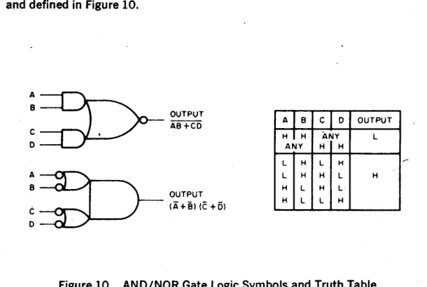
TTL AND/NOR GATE
With a few modifications; the basic TTL NAND gate can perform an ANDI
NOR function useful in exclusive OR, coincidence, line selection and NOR gating operations. The modified circuit is shown in simplified form in Figure 9.
r---~~--~---~~---o +vcc
A I
c
o [image:35.378.28.333.293.498.2]~--... ~ OUTPUT
Figure 9 TTL AND/NOR Gate Simplified Schematic
Circuit Operation: The basic elements of the TTL NAN D gate are used· with-out modification. The phase-splitter (Q2) is paralleled with an identical transistor (Q6), also controlled by multiple-emitter input transistor which receives two additional inputs, C and D. When either of the input pairs are high, the phase inverter operates to switch the output voltage low. Circuit performance is essentially identical to the TTL NAND circuit.
AND/NOR Logic Symbol: The logic symbols for the AND/NOR gate are shown and defined in Figure 10.
:~O.UTPUT
AB+CDC •
o
A B C 0 OUTPUT H I H ANY L
ANY H H
L H L H
L H H L H
H L H L
H L L H
A;D-8
OUTPUT
~. (A+B)
(e
+O)Figure 10 AND/NOR Gate Logic Symbols and Truth Table
:~OUTM
:=[>-OUTPUT
AND/NOR INPUTS TIED RESULTING NOR SYMBOL
Figure 11 NOR Connection of AND/NOR Gate
NAND GATE FLIP-FLOPS
RS Flip-Flop: A basic Reset/Set flip-flop can be constructed by connecting two NAND gates as shown in Figure 12.
SET----Ot
PREVIOUS INPUT
RESULT
STATE CONDITION
1 0 SET RESET 1 0
L H L H H L
H L H L L H
L H H H N.O CHANGE
H L H H NO CHANGE
H L L H NO CHANGE
o L H H L NO CHANGE
RESET---<Y L H L L
H* H*
H L L L H* H*
~Ambiguous state: In practice the input that stays lo~ longest will assume control.
Figure 12 RESET/SET NAND Gate Flip-Flop
CLOCKED NAND GATE FLlP·FLOPS
The Reset-Set flip-flop can be clock-synchronized by the addition of a two-input NAND gate to- both the set and the reset two-inputs. (See Figure 13.) One of the inputs of each NAND is tied to a common clock or trigger line.
SET
CLOCK
o RESET
[image:36.378.29.341.35.318.2]A change of state is inhibited until a positive clock pulse is applied. The ambiguous case will result if both the set and reset inputs are high when the clock pulse occurs.
M SERIES GENERAL-PURPOSE FLIP-FLOPS
Two types of general·purpose flip-flops are available in the M Series, both of which have built-in protection again'st the ambiguous state characteristic of NAND gate flip·flops.
FLIP-FLOP CLOCK INPUT SYMBOLS
The D type flip·flop is a true leading (positive going voltage) edge triggered flip-flop and the D input is locked out until the clock input returns to low. The symbol to i-ndicate this function will be as follows;
o
TYPE F:LIP FLOP CLOCKThe operation of the J-K type flip-flop is to transfer the information present at the J and K inputs just prior to and during the clock pulse to the master flip-flop when the threshold is passed on the leading (positive going voltage) edge of the clock pulse. The information stored in the master flip-flop is transfered to the slave flip-flop, and consequentially to the outputs, when the threshold is passed on the trailing (negative going voltage) edge of the clock pulse. The symbol to indicate this function will be as follows;
J K TYPE FL I P FLOP CLOCK
o
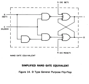
Type Flip-Flop: The first of these is the 0 type flip-flop shown in Figure 14 In this element, a Single-ended data input (D) is connected directly to the set gate input. An inverter is provided between the input line (D) and the reset input. This ensures that the set and reset levels cannot be high at the same time.o
SLOGIC SYMBOL
r---D - - -...
- - - i
(SET)C----+---~
(CLOCK)
I
I
I
I
L
NAND GATE EQUIVALENT
S (DC SET)
>--'-'---0
I
----~
R (DC RESET)
SIMPLIFIED NAND GATE EQUIVALENT
Figure 14. D Type General Purpose Flip-Flop
The flip-flop proper employs three-input NAND gates to provide for dc set and reset inputs.
D type flip-flops are especially suited to buffer register, shift register and binary ripple counter applications. Note that D type devices trigger on the leading (or positive going) edge of the clock pulse. Once the clock has passed threshold, changes on the D input will not affect the state of the flip-flop due
to a lockout circuit (not shown). .
[image:38.378.44.336.72.349.2]UMASTER·SLAVE J·K FLlp·FLOP"
The two unique features of a J-K flip-flop are: A) a clock pulse will not cause any transition in the flip-flop if neither the J nor the K inputs are enabled during the clock pulse, and B) if both the J and the K inputs are enabled during the clock pulse, the flip-flop will complement (change states). There is no indeterminate condition in the operation of a J-K flip-flop.
A word of caution is in order concerning the clock input. The J and K inputs must not be allowed to change states when the clock line is high, the output will complement on the negative going voltage transition of the clock. It is for this reason that the clock line must be kept low until it is desired to transfer information into the flip-flop and no change in the states of the J . and K inputs should be allowed when the clock line is high.
The J-K flip-flops used are master-slave devices which transfer information to the outputs on the trailing (negative going. voltage) edge of the clock pulse_ The J-K flip-flop consists of two flip-flop circuits, a master flip-flop and a slave flip-flop. The information which is present at the J and K inputs when the leading edge threshold is passed and during the clock high will be passed to the master flip-flop (The J and K inputs must not change after the leading edge threshold has been passed). At the end of the clock pulse when the threshold of the clock is passed during the trailing (negative going voltage) edge, the information present in the master flip-flop is passed to the slave flip-flop. If the J input is enabled and the K input is disabled prior to and during the clock pulse, the flip-flop will go to the "I" condition when the trailing edge of the clock occurs. If the K input is enabled and the J input is disabled prior to and during the clock pulse, the flip-flop will go to the "0" condition when the trailing edge of the clock pulse occurs. If both the J and K inputs are enabled prior to and during the clock pulse, the flip-flop will complement when the trailing edge of the clock pulse occurs. If both the J and K inputs are disabled prior to and during the clock pulse, the flip-flop will remain in whatever condition existed prior to the clock pulse when the trailing edge of the clock pulse occurs. ~
J INPUT - - + - - f
I OUTPUT
CLOCK
o OUTPUT
K INPUT --+---f
Figure 16 shows a functional block diagram of a master slave J-K flip-flop using NAND gates_ Gates C and 0 are the master flip-flop. Gates G and Hare the slave flip-flop. Gates A and B are the steering network of the master flip-flop and the steering network for the slave flip-flop is comprised of gates E, F, and 1. The 1 output of the master flip-flop is point X. The operation of the flip-flop will be studied by examining the "1" to "0" transition of the flip· flops, with both the J and the K inputs enabled with a HI level before the clock pulse. When the leading edge of a HI clock pulse occurs, gate B will be enabled with three HI inputs. This will provide a RESET signal for the master flip-flop which will then go to the :'0" condition. The slave flip-flop remains in the "1" condition while the clock pulse is HI because gate I is providing a LO signal to both gates E and F, thereby blocking inputs to the slave flip-flop. When the trailing edge of the clock pulse occurs, gate F will be enabled with a HI level at both its inputs and a RESET signal will be provided to the slave flip·flop, which will then go to the "0" condition. The next clock pulse, with both the J and K enabled, would cause the master flip-flop to go to the "1" condition on the leading edge of the clock pulse and cause the slave flip·flop to go to the "1" condition on the trailing edge of the pulse. Figure 16 is a truth table for the J·K flip-flop showing all eight possible initial conditions.
INITIAL CONDITIONS FINAL CONDITIONS
OUTPUTS INPUTS OUTPUTS
1 0 J K" 1 0
L H L L L H
l H l H L H
L H H L H L
L H H H H L
H L L L H L
H L L H L H
H L H L H L
H L H H L H
UNUSED INPUTS (GATES AND FLlP·FLOPS)
Since the input of a TTL device is an emitter of a multiple·emitter transistor, care must be exercised when an input is not to be used for logic signals. These emitters provide excellent coupling into the driving portions of the circuit when left unconnected. To insure maximum noise immunity, it is necessary to connect these inputs to a source of Logic 1 (High). Two methods are recommended to accomplish this:
1. Connect these inputs to a well filtered and regulated source of +3 volts. Pins U1 and VI are provided on the M1l3, M1l7, M1l9, Ml2l, M617, and
M627 for this purpose.
2. Connect these inputs to one of the active inputs on the same gate. This results in a higher leakage current due to the parallel emitters and should be considered as an additional unit load when calculating the loading of the driving gate.
Connection of unused inputs to the supply voltage, Vee, is not advisable, since power supplies are subject to transients and voltage excursions which could damage the input transistor.
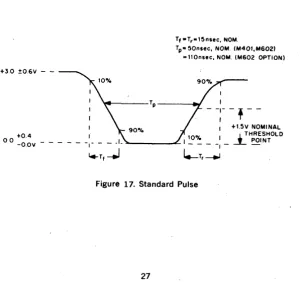
TIMING CONSIDERATIONS
Standard Timing Pulse: In digital system design, a reference for system timing is usually required. The M Series modules M401 or M405 produces a standard pulse which provides such a reference. The standard pulse derived from each of these two modules is shown in Figure 17.
+3.0 :t06Y -
-Tf- T,.'5nsec, NOM.
Tp.50nsec, NOM. (M401,M6021 '" 11 Onsec, NOM. (M602 OPTION)
I . . _______ ~ __ - -_ _ ~ 1
-
-;-
-
,
--I I +1.5Y NOMINAL
+0.4 I 1 _'0"1. _ __ I _ 1 THpRJi~~OLD
00 -O.OY - - - -1- - - .1. ---~ I - L .
[image:41.381.32.336.277.559.2]~Tf...J
I.-Tr--.JNAND Gate and Power Amplifier Propagation Delays: The standard pulse (Figure 17) is distributed throughout a system in negative form to maintain the leading edge ~ntegritY. (Since the TTL gate drives current in the logic
o
state, the falling edge is more predictable for timing purposes.) However, the standard pulse is of the wrong polarity for use as a clocking input to the type D and J-K flip-flops, requiring the use of a local inverter. Ordinarily, a NAND inverter is adequate. Where high fan-out is necessary, a M617 Power NAND is preferred.For applications requiring both high fan-out and critical timing the M627 Power Amplifier is available. This module contains extremely high-speed gates which exhibit turn-on times differing by only a few nanoseconds.
Simultaneity is desirable in clock or shift pulses distributed to extended shift registers or synchronous counters.
Delays introduced by inverting gates and power amplifiers are illustrated in Figure 18. (Delays are measured between threshold points.)
STANDARD I
PULSE
NAND OR POWER NAND GATE
I I
I I
j.-ton--.j j..-toff-l I I_~-.... I
I
I j..toff-i I ,
,---- I r-tonPOWER II /
AMPLIFIER M621
- - - - I
I
DELAY (NANOSECONDS)
ton toff
TYP. MAX. TYP. MAX.
18 29 8 15
7 - 5
[image:42.378.83.329.219.498.2]Flip-Flop Propagation Delays: 0 type flip-flops trigger on the leading or rising edge of a positive clock pulse; the propagation delay is measured from the threshold point of this edge. The set-up time of the 0 flop is also measured from this threshold point. Data on the 0 input must be settled at least 20 nanoseconds prior to the clock transition. The advantage of the D-flip-flop, however, is that the leading edge triggering allows the flip-flop AND gates to propagate while the clock pulse is still high. Figure 19 illustrates this situa-tion.
CLOCK
o TYPE FLIP FLOP OUTPUT
"'20 •• ofoIIl"~--N5S0EC~ I NSEC I
I ~~T I '
I I I
+
~30~
NSEC I
- - - ,
Figure 19. 0 Type Flip·Flop Timing
JK type flip-flops are, in effect, trailing edge triggering devices as explained previously. The only restriction on the J and K in-puts is that they must be settled by the time that the rising edge occurs. Timing is shown in Figure 20.
!.--
J AND K INPUTS MUST BE I STABLE BY THIS TIME ITRIGGER
PULSE
__ 1
\
----FLlP- FLOP OUTPUT
I
---.'
Il.-
I/
---~
Figure 20. J·K Flip-Flop Timing
[image:43.380.45.330.337.559.2]When using the dc Set or Reset inputs of either flip-flop type, propagation delays are referenced to the falling edge of the pulse_ This is due to the inverted sense of these inputs_ When resetting ripple type counters (where the output of one flip-flop is used as the trigger input to the next stage) the reset pulse must be longer ttian the maximum propagation delay of a single stage_ This will ensure that a slow flip-flop does not introduce a false transi-tion, which could ripple through and result in an erroneous count_
[image:44.379.37.331.186.421.2]One-Shot Delay: Calibrated time delays of adjustable duration are generated by the M302 Delay Multivibrator. When triggered by a level change from a logical one to a logical zero, this module produces a positive output pulse that is adjustable in duration from 50 to 750 nsec with no added capacitance. Delays up to 7.5 milliseconds are possible without external capacitance. (See M302 specification.) Basic timing and the logic symbol are shown in Figure 21. The 100 picofarad internal capacitance produces a recovery time of 30 nsec. Recovery time with additional capacitance can be calculated using the formula;
OUTPUT , (TYPICAL)
tr Nanoseconds
=
30 C Total (Picofarads) 100.~D
0.5.,
~OUTPUT
L-ir.J LOGIC SYMBOL
I I
'---tr--+:
, - - -... ~ ... ~
:
I
- + 1 14----50 nsec TYPICAL
: r--
50 TO 750 ".H<~
I I ~ ... - -
J
~:
-
.~,:---~-I I TIMING
figure 21. One-Shot Delay Timing and Logic Symbol
SYSTEM OPERATING FREQUENCY
",
1. A standard clock pulse width of 50 nsec is assumed. -This period is measured from the threshold point of the leading edge to the threshold point of the trailing edge.
2. One flip-flop propagation delay of 35 nsec from the trailing edge of the clock pulse to the threshold point of the final state of the flip-flop is allowed.
3. Two gate-pair delays of 30 nsec each are assumed. (A gate-pair consists of two inverting gates in series.) Two gate-pair delays are usually re-quired to perform a significant logic function with a minimum of parallel operations. The two gate-pair delays total 60 nsec.
[image:45.379.40.346.200.482.2]The time necessary to perform these operations before the next occurrence of the clock pulse is the sum of the delays; 50"+ 35 + 60, or 145 nsec. Allow-ing 20 nsec for variations within the system, the resultAllow-ing period is 165 nsec, corresponding to a 6 MHz clock rate. This timing is demonstrated in Figure 22.
GATE GATE
CLOCK F/F PAIR PAIR
WIDTH DELAY DELAY DELAY IDLE t--- 50 - . . - 35 ... 30 ~ 30 ...,.. 20 4j
nsec nsec nsec nsec nsec,
I I I I I I
I
CLOCK
o
_
_ f:
JK FLIP - FLOP
o I
_ _ _
I:
GATE PAIR'
o j
o_
~_f:
GATE PAIR 2 _
Figure 22. Delays Determining System Operating Frequency
Substitution of a D type flip-flop results in a similar timing situation. In a system using both D and J-K flip-flops, note that the 0 flip-flop triggers on the leading edge of the clock pulse and the J-K flip-flop triggers on the trailing edge. When calculating system timing using D flip-flops, remember that the flip-flop inputs must be settled at least 20 nsec prior to the occurrence of the clock pulse.
M SERIES LOGIC AND CONTROL MODULES
Modules in this section are organized into six functional categories:
M1l3 M1l5 M1l7 M1l9 M133 M135 M137 M139 M1l31 M141 Ml103 M1307 M121 M1l6 M1l2 M1125 MIll M611 M165 M205 M206 M207 M246 M202 M203 M2001 M204 M245 M248 M239 M2500 M3020 M306 M501 M310 M401 'M403 M404 M405 M602 M671 M521 GATES
NAND GAtes NAND Gates NAND Gates NAND Gates
Two-Input NAND Gates Eight 3-lnput NAND Gates NAND Gates
Three 8-lnput NAND Gates Open-Call ector NAN D Gates NAND/OR Gates
Two-Input AND Gates Four-Input AND Gates AND/NOR Gates Six 4-lnput NOR Gates NOR Gates
Exclusive-OR Gates Inverter
Inverter Eight Buffers
FLIP-FLOPS AND REGISTERS
General Purpose Flip-Flops General Purpose Flip-Flops General Purpose Flip-Flops Five OoType Flip-Flops Triple J-K Flip-Flop 'Eight R/S Flip-Flops Tri-State Flip-Flop
General Purpose Buffer and Counter Dual4-Bit Shift Register
Dual 4-Bit Multipurpose Shift Regi$ter Four-Bit Counter/Register
MOS Memory
TIME RELATED
Integrating One Shot Integrating One Shot Schmitt Trigger Delay Line Variable Clock RC Multivibrator Clock Crystal Clock
MI6I MI63 M230 M236 M237 M238 MI59 MI91 MI55 MI70I MI7I3 MI68 M162. M040 M050 M060 M617 M627 M660 M002 M594 M598 M706 M707 M906 M7389 M7390 M9970 INMERIC
Binary to Octal/Decimal Decoder Binary to Decimal Decoder
Binary to BCD and BCD to Binary Converter 12-Bit Binary Up/Down Counter
3-Digit BCD Up/Down Counter
Dual 4-Bit Binary Synchronous Up/Down Counter Arithmetic/logic Unit
AlU look-Ahead logic 4-line to I6-line Decoder Data Selector
I6-line to I-line Data Selector 12-Bit Magnitude Comparator Parity Circuit
LOGIC AMPLIFIERS
Solenoid Driver Indicator Driver Solenoid Driver
4-lnput Power NAND Gates NAN 0 Power Amplifier Positive level Cable Driver
MISCELLANEOUS
logic HIGH Source EIA/CCITT level Converter
One-Channel Transmit/Receive Optic-Coupled Cur· rent Isolator
Teletype Receiver Teletype Transmitter Cable Terminator
M113, MIlS, M117, Ml19
NAND GATES
GATES
Length: Standard Height: Single
Width: Single
~
AlCl,O 1 B1
~
DlFl 10
t Et
~
D2F2 '0 1 E2
~
HlKt 10 1 Jt
~
H2K2 tO 1 J2
Mt13 2-INPUT NAND GATES
Volts +5 +5 +5 +5 GND
Power
mA (max.) 71 M1l3 41 M1l5 41 M1l7 19 M1l9
M SERIES
~
PI 51 10 I Rt~
~
~
T2V2,0 t U2
B :::
s
' 81, C!
S
1 E2
I F2
S
lFl Et~
Io'-H;.;.1 _ _ - r _ _ -
S
1 KZ
1 L2
E3
I I I I MlE1
t Rtt S1
M115 3-INPUT NAND GATES
M1t9 a-INPUT NAND GATES
These modules provide general-purpose gating for the M Series, and are most commonly used for decoding, comparison, and control. Each module per-forms the NAND function (.
B·
c
·--N),
depending upon the number of inputs.APPLICATIONS • Logic gating FUNCTIONS
MIl3-Ten two-input NAND gates that also may be used as inverters. Mll5-Eight, three-input NAND gates.
MIl7-Six, four-input NAND gates. MIl9--Three, eight-input NAND gates.
Unused inputs on any gate must be either connected to a used input or re-turned to a source of logic HIGH, for maximum noise immunity. In theMIl3, MIl7, MIl9, M121, M6l7 and M627 modules, two pins are provided (UI and VI) as source of +3 volts for this purpose. Each pin can supply up to 40 unit loads. MI03, MIll and M002 provide additional sources of logic HIGH level.
SPECIFICATIONS
M133
TWO-INPUT NAND GATES
GATES
Length: Standard
Height: Single
Width: Single
C,
~
AI1 81 . 12
~
OIFI 12
1 EI
F2
~
DZ1 E2 . 12
~
HIKI 12 1 JI
~
HZK2'2 1 J2
Power
M SERIES
~
L1'. Nf 12 1 M
~
__N?~
~
PI Sf 12 1 Rt~
P2 S2'2
1 R2
~
TV2 ,2 1 U
Volts
+5
GND
mA (max.)
160
Pins A2
e2, Tl
This module provides general-purpose high-speed NAND gating.
APPLICATioNS
The high-speed characteristic of these gates frequently will solve tight timin
J
proble~s in complex systems.SPECIFICATIONS
MI3S
GATES
8 3-INPUT NAND GATES
M ,SERIES
Length: Standard Height: Single Width: Single
1
,3 EI 41.3_ FI : 1.3 HI ._
)
,01 @)
) J1
@)
)
,N'@)
)
,"' @)
Volts
+5
GNDPower rnA (max.) 100
)
~J2
~f-~2-2
- :--r---)
Pins A2
C2. T1
[)
)
H2
@]
. 1 2,M2@]
.52
@]
VI
@)
. 1 2
The M135 module consists of eight high-speed, 3-input, positive logic NAND gates. It is pin-compatible with the Mll5 module.
APPLICATIONS
• Logic gating
SPECIFICATIONS
Maximum propagation delay to a logic HIGH or LOW is 10 ns.
MI37
SIX 4 INPUT NAND GATES
Length: Standard
Width: Single
Height: Single
Volts
+5V
GND
Power mA (max.) 100 mA
Pins A2 C2. Tl
GATES
M SERIES
\
The M137 Module consists of six high-speed, 4-input positive logic NAND' gates that can be used in many logic gating applications.
Maximum propagation delay to.a logic High or Low is 10 p,s.
M139
3 8-INPUTNAND GATES
Length: Standard Height: Single Width: Single
Volts
+5
GND
Power mA (max.) 50
Pins A2
C2,Tl
GATES
M SERIES
The M139 module consists of three high-speed, 8-input, positive logic NAND gates. Pins Ul and VI provide two separate logic HIGH sources (+3 V,) each capable of holding up to 50 unused M Series inputs HIGH.
APPLICATIONS
• Logic gating
SPECIFICATIONS
Maximum propagation delay to a logic HIGH or LOW is 10 ns.