2125
PERFORMANCE ANALYSIS OF THROUGH SILICON VIA’S
(TSV’s)
SANATH KUMAR TULASI1, M. SIVA KUMAR2, P. AMRUTHALAKSHMI3, M. AKHILA3,
M. TEJA4, G. MOHAN SHANKAR4.
1
Assistant Professor, Department of ECE, KLUniversity, Vaddeswaram, AP, India
2
Associate Professor, Department of ECE, KLUniversity, Vaddeswaram, AP, India
3,4
BTech Students, Department of ECE, KLUniversity, Vaddeswaram, AP, India
E-mail: [email protected], [email protected], [email protected],
[email protected]* ,[email protected], [email protected]
ABSTRACT
At present, the 3-D IC integration utilizes Through Silicon Vias (TSV's) and it increased tremendous energy. The structure of the TSV composed of Cu, isolating liner and the silicon substrate. The isolating liner is encompassed signal TSV to stay away from signal leakage from TSV to the silicon substrate. In the conventional TSV structures, Sio2 is utilized as an isolating liner on account of its material compatibility with thesilicon substrate. To contrast to that several researchers had reported the issues of Sio2. Due to the high dielectric constant to such an extent that it brings about increasing of delay. Subsequently, Sio2 is not appropriate for elite applications. In this paper, we utilized polymer liner as isolating liner in place of Sio2. We simulated the performance analysis for both conventional and proposed TSV structures by varying radius and height of TSV. The proposed TSV structure simulation shows better results compared to conventional TSV structure.
Keywords: Delay, Height, Power, Radius, Through-Silicon Via (TSV).
1. INTRODUCTION
According to Moore's prediction, the number of transistors that are to be fabricated on a chip gets doubled for every eighteen months. Due to breakneck increase in thecount of transistors fabricated, the 2D IC integration is getting complicated. Subsequently, it becomes a hard nut to crack for the design engineers. To overwhelm this hectic task engineer’s instigated 3D IC integration technology. [2]In the preface of 3D IC integration process wirebonds and flipchips are used for a certain time period and then replaced by TSV's which are considered to
be the predominant method for
interconnection[8]. In the semiconductor
manufacturing sector, these TSV's have been the most expeditious developing technology and are used for multi-chip integration and packaging techniques [13].
TSV is a vertical electrical association [16] going totally through a silicon wafer.TSVs are a superior interconnect methods utilized as a contrasting option to wire-security and flip chips
[18] [7] to make 3D bundles and 3D incorporated circuits, contrasted with options. Short pitch in between the signal TSV and ground TSV, crosstalk analysis [3] which causes achange in the delay becomes important. [1] In past, many approaches have been suggested for designing TSV’s. TSVmodelinghas been suggested for a3D package of an IC. In the proposed model delay and powerconsumption have been reduced by varying the radius of a signal TSV and the height of TSV that is to be fabricated [21].
2126 models are simulated using T-Spice [21] [9] and
comparison of performance analysis of
TSVmodeling is done.
2. DESIGN METHODOLOGY
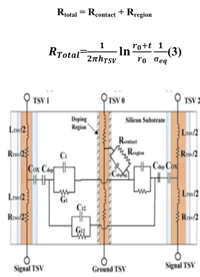
In 2D IC integration, fabrication is done in a horizontal manner[4] whereas, in 3D IC integration, fabrication is done in avertical manner where the usage of thearea is reduced. In fabricating a 3D IC and 2.5D IC[6] TSV are used. TSV’s are the basic structures which act as an electrical connectivity between two dies which are placed on a silicon wafer. The basic conventional circuit which is proposed in [1]. In this circuit,the TSV’s have two inductors and two resistors. The circuit is as in Fig 1. As the signal, TSV has an oxide layer so an oxide capacitance (Coxide) and a depletion layer so a
depletion capacitance (Cdepletion) exists between
the signal and ground TSV associated witha signalTSV.
There exists a contact resistance (Rcontact)
=
(1)
In the above equation i.e., to calculate contact
resistance we should know hTSV( height of TSV).
is concentration of contact resistance which is a constant value [1].
is the radius of doping region which is formed around the signal TSV [20].
The resistance for that region(Rregion).To
calculate Rregion, isthe doping region resistivity constant
Where it can be given as / and the
doping region resistance can be calculated over the thickness of doping region [1].
!
"
=
#
% $=
&!
%(2)
These two resistance‘sconstitute as a total resistance acting across the ground TSV [1], that is by combining the equations (1) and (2).
Rtotal = Rcontact + Rregion
'
=
&!
% ( [image:2.612.320.517.88.361.2])
(3)
Fig 1: Structure of TSV
By equalizing the total resistance and summation of contact resistance and doping
region resistance ( *can be obtained as below
[1].
(
)=
&!+ % ,%(&!+ - ,
(4)
The conductivity depends on the concentration of doping which creates doping region, so the doping capacitance is required. It can be computed as
. /
=
&!+ % ,0(5)
Using transmission line model the
resistance, capacitance and inductance
parameters are calculated forTSV’sand silicon substrates.
1
2=
3
4
&! 5
'6 ,
2
4
&! +
' '2'2
, , 8 2
2127
Where Lij is the inductance of TSV.9 is the
relative permeability of free space.
&: is the space between two TSV’s.
0,1,2 are the number representations of TSV’s.
& is the distance between the first signal TSV
and ground TSV. & is the distance between
ground TSV and second signal TSV. & is the
total distance between two signal TSV’s.
Parasitic capacitance existsbetween
both the signal and ground TSV [15] [14]. Coupling capacitance and resistance are between TSV’s can be drawn out as follows.
C=
4 0
1
;(7)
G=
4
(
1
;(8)
Where
<
= and are the constant‘s for dielectricmaterial and conductivity of silicon substrate [1].
As the radius of tsv decreases the value of Rtsv that is the resistance of the signal tsv’s
and ground tsv’sare increased and with a decrease in Ltsv which is an inductance value of
through silicon via’s [17]. The oxide capacitance between signal and ground tsv remains constant. The capacitance of silicon decreases and the inverse of resistance decreases. Now considering the height as varying parameter the values are altered correspondingly as that are to be mentioned below.
The values for a conventional circuit are obtained with the help of mathematical computational software using the formulae which are required for comupting the values. And these values are substituted in the circuit and simulated using T Spice simulator.
The resistance of tsv decreases with adecrease in height and the inductance of tsv’s are increased and the oxide layer capacitance, silicon layer capacitance increases. The inverse of resistance values decreases. The total resistance increases and the doping capacitance also increases for thedecrease in radius and height. As a result of the performance parameters delay and power decreases which contributes to the maximum reliability[12] and reduced noise margin which helps for proper transmission of data [19] [11].
3. RESULTS AND SIMULATIONS
In this module, we discuss the simulation results and observe the performance of the proposed model in [1]. The radius and height of the TSV’s are varied accordingly and the effect of delay and power in the circuit is analyzed[10].
3.1. Simulation Analysis
Initially, the height of the TSV is kept constant assuming as 100 µm and the radius is varied from 20 µm to 10 µm and the change in delay and power is observed. Next, the radius of TSV is kept constant at 10 µm and the height of the TSV is varied from 100 µm to 50 µm and the variations in performance parameters are also observed.
Fig2:Structure of TSV with radius 20 µm and height 100 µm
2128 Fig3: Waveforms obtained when radius and height are
20 µm, 100 µm
By observing the waveforms obtained the input and output waves resemble the same with the difference in delay and power waveform is obtained as shown in Fig 3.
Fig4: Structure of TSV, when radius and height are 10 µm, 100 µm
When the radius is 10µm and heightare 100 µm the respective values of inductors, capacitors and resistance are obtained they are connected in the simulatingenvironment as shown in Fig 4.
Fig5: Waveforms obtained when radius is 10µm and height100µm
By perceiving the waveforms obtained the input and output waves correspond to bealike with thedifference in delay and power waveform is obtained as shown in Fig5.
Fig6: Structure of TSV, when radius 10 µm and height 50 µm
2129 Fig7: Waveforms obtained when radius is 10 µm and
height 50 µm
By observing the waveforms obtained the input and output waves bear a resemblance to the alike with thedifference in delay and power waveform is obtained as shown in Fig7.
3.2. Comparison Analysis
Table 1: Delay analysis for TSV Structure by varying radius
Delay when radius is varied
Radius(m) Height(m) Delay(s)
20 µ 100 µ 14.1334p
[image:5.612.326.533.500.704.2]10 µ 100 µ 04.6700p
Table 2: Power analysis for TSV Structure by varying radius
Power when radius is varied
Radius(m) Height(m
)
Avg Power(W)
Max power(W)
20 µ 100 µ 1.4229e-4 1.8313e-3
10 µ 100 µ 5.9309e-3 5.3052e-1
Table 3: Power Delay Product analysis for TSV Structure by varying radius
Power Delay Product when radius is varied
Radius(m) Height(m) PDP(Ws)
20 µ 100 µ 2.009e-15
10 µ 100 µ 2.769e-14
Table 4: Delay analysis for TSV Structure by varying height
Delay when height is varied
Height(m) Radius(m) Delay(s)
100 µ 10 µ 04.6700p
50 µ 10 µ 04.2022p
Table 5: Power analysis for TSV Structure by varying radius
Power when Height is varied Height(
m)
Radius( m)
Avg Power(W) Max
Power(W)
100 µ 10 µ 5.93079e-003 5.3052e-01
50 µ 10 µ 2.981777e-003
3.1865e-001
Table 6: Power Delay Product analysis for TSV Structure by varying radius
Power Delay Product when Height is varied
Height(m) Radius(m) PDP(Ws)
100 µ 10 µ 2.769e-14
50 µ 10 µ 1.21515e-14
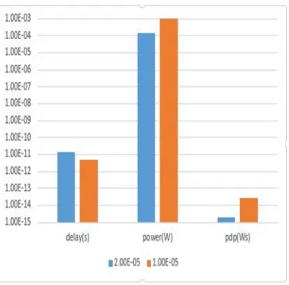
The execution parameters are compared and tabulated in tables 1-6. In this muniment, the parameters considered are delay, power and product of those two and these are compared using bar graphs. In the Fig 8, the similitude of two different radii for the parameters like delay, power and power delay product are plotted and represented.
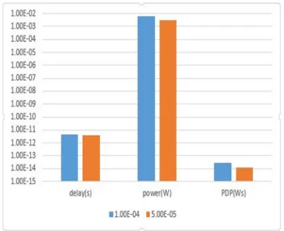
2130 In the shownfig 8, 9, the similarities between the parameters (delay [11], power and power delay product) are observed for unlike values of heights.
Fig 9: Comparison graph between parameters for different heights
The graphs in fig 8,9depict the information of different parameters for different
radius and heights. The three different
parameters are Delay, Power and PDP (Power delay Product).The first graph compares the parameters with the two different radii 20µ and 10µ denoted with two different colors blue and orange. The delay for radius 20µ is slightly above 10p in Y-axis and the delay for the radius 10µ is close to 10p which is slightly less to the radius 20µ.The power parameter for radius 20µ is at 100µ and for radius, 10µ reached the top 0.001 and is higher to 20µ and same with PDP, 20µ is lower compared to 10µ.
20µ is minutely above 1.00f radius and 10µ is above 0.01p which is half near to 1.00E-13. In the first graph, the radius 20µ is only higher in delays and less in other parameters. In the second graph, the y-axis has different heights and it also has three parameters same as the first graph and it is also a comparison between two different heights 100µ and 50µ.
The delays for both heights are almost same and a half near to 10p,100µ is negligibly higher to 50µ and power for 100µ height is very near to 0.01 and it is the highest and the other height 50µ is slightly less and a half near to 0.01. The PDP for 100µ is over 0.01p and for 50µ is
0.01p approximately. The height 100µ has the higher values for the given parameters.
3.3 Merits and Demerits
The merits of TSV(through Silicon Via) are it gives better performance in terms of electrical i.e., it consumes less power so the circuit has lower power consumption. Bandwidth is the bit-rate of amount of information consumed. There are types of bandwidth network bandwidth and data bandwidth. Network bandwidth is the rate of information shared on a network which is not necessary in this context. Where as coming to data bandwidth is the amount of data that can transmitted at a time. TSV’s provide a wider data bandwidth where a large amount of data can be transmitted in single time. These also provide a very high density. It offers low cost when compared to another electrical connectivities and weighs in very small quantity.
The demerits of TSV’s are discussed as follows. As the circuit becomes complex the cost of the circuit increases. TSV aspect ratio is low which reduces the difficulty in processing, have a high yeild rate and leads to short process time. In fabricating a TSV there are via first formation [2], via middle [2] and via-last [2] which reduces the fabrictaion damage. Problems caused with bump-less contact which can be avoided by providing a bump contact.
TSV’s are mainly used in memory devices, processors and sensors. These are especially used in RAM (Read Only Memory) like SRAM, DRAM, flash memories and so on. Used in sensors like image sensors, are those sensors that convey information about the presence of image.
4. CONCLUSION
2131 constant height (100µm). Subsequently, the values of delay and power are examined at height (100µm and 50µm) withconstant radius(10µm). The power-delay product is evaluated at appropriate values. These results are simulated using T-Spice.
REFERENCES
[1] De-Cao Yang, Jianyong Xie, Xing-Chang
Wei, Er-Ping Li ”Rigorous model for TSV with ohmic contact with silicon interposer” IEEE trans received on March 15, 2013, revised May 30, 2013.
[2] Brajesh Kumar Kaushik,Manoj Kumar
Majumder, and Vobulapuram Ramesh Kumar,Carbon Nanotube based 3-D interconnects- a reality or a distinct dream”published in IEEE in the year 2014
[3] C. Xu, R. Suaya, and K. Banerjee, “Fast
extraction of high-frequency parallel
admittance of Through-Silicon-Vias and their capacitive coupling noise to active regions,” in Int. Microw. Symp. Dig., 2012, pp. 1–3.
[4] E. Engin and N. S. Raghavan,
“Metal-semiconductor (MES) TSVs in 3D ICs: Electrical modeling and design,” in Proc. IEEE Int. 3D Syst. Integr. Conf., 2012, pp. 1–4.
[5] M. Swaminathan and K. J. Han,
“Electromagnetic modeling of through-silicon via (TSV) interconnections using cylindrical modal basis functions,” IEEE Trans. Adv. Packag., vol. 33, no. 4, pp. 804-817, April 2010.
[6] B.Xie , , K.J.Han , M.Swaminathan J. Xie “
Coupling Analysis of Through-Silicon Via (TSV) Arrays in Silicon Interposers for 3D Systems”in IEEE trans,2011.
[7] J. Kim, J.Cho J.S.Pak “High-Frequency
Scalable Electrical Model and Analysis of a Through Silicon Via (TSV)” IEEE Trans. Compo., Packag, Manuf. Techno., vol. 1, no. 2, February 2011.
[8] A.C.Hsieh, , M.T. Chang, T.T.Hwan ” TSV
Redundancy: Architecture and Design Issues in 3D IC” in February 2015.
[9] W.S.Zhao, S.ChenG.Wang, J.Zheng,
“Transient Analysis of Through-Silicon Vias in Floating Silicon Substrate” IEEE Trans. Electro. Compat, vol. 59, no. 1, February 2017.
[10]A.Eghbal, P.M. Yaghini, “Analytical Fault
Tolerance Assessment and Metrics for TSV-based 3D Network-on-Chip ”in IEEE trans.comp.,2015.
[11]B.Vaisband and E.G.Friedman “Noise
Coupling Models in Heterogeneous 3-D ICs”in IEEE Trans. VLSI. Sys., vol. 24, no. 8, August 2016.
[12]M.Jung, , D.Z. Pan, J.Mitra and S.K.Lim”
TSV Stress-aware Full-Chip Mechanical Reliability Analysis and Optimization for 3D IC”in Jun 05-10 2011, San Diego, California, USA.
[13]Xi.Wang, Mi.Xiong, Z.Chen, “Wideband
Capacitance Evaluation of Silicon–
Insulator–Silicon Through-Silicon-Vias for 3D Integration Applications” in IEEE Electro.,vol. 37, no. 2, February 2016.
[14]T.Bandyopadhyay, K.J.Han, D.Chung,
“Rigorous Electrical Modeling of Through Silicon Vias (TSVs) with MOS Capacitance Effects ” in IEEE trans. Compo., Packag. Manuf. Techno., vol. 1, no. 6, June 2011.
[15]D.Z. Pan, S.K.Lim “Design for
Manufacturability and Reliability for TSV-based 3D ICs” in IEEE trans.2015.
[16]I.Savidis, S.M.Alam , A.Jain “Electrical
modeling and characterization of through-silicon vias (TSVs) for 3-D integrated circuits”in Microelectr. Journ.41 (2010) 9– 16.
[17]Z.Xu and J.Q.Lu “High-Speed Design and
Broadband Modeling of Through-Strata-Vias (TSVs) in 3D Integration”in IEEE Trans.,Compo, Packag., Manuf.,Techno, vol. 1, no. 2, February 2011.
[18]T.Jiang , S.Ryu “Measurement and analysis
of thermal stresses in 3D integrated structures containing through-silicon-vias” in Microelectr. Reliab., 53 (2013) 53–62.
[19]I.Ndip, K.Löbbicke “High-Frequency
Modeling of TSVs for 3-D Chip Integration and Silicon Interposers Considering Skin-Effect, Dielectric Quasi-TEM and Slow-Wave Modes” in IEEE Trans.Compo, Packag.Manuf., Techno, vol. 1, no. 10, October 2011.
[20]D. Malta, E. Vick, S. Goodwin “Fabrication
of TSV-Based Silicon Interposers” in Intern.,confer.,pap.,RTI .,USA.,2012.
[21]G R K Prasad etal; “Router design using