IJSRST1841231 | Received : 10 Feb 2018 | Accepted : 20 Feb 2018 | January-February-2018 [ (4) 2: 1130-1136]
© 2018 IJSRST | Volume 4 | Issue 2 | Print ISSN: 2395-6011 | Online ISSN: 2395-602X Themed Section: Science and Technology
1130
Design of CMOS Phase Locked Loop
Kaviyadharshini SivaramanPG Scholar, Department of Electrical and Electronics Engineering, Dr. Mahalingam College of Engineering and Technology, Pollachi, Tamil Nadu, India
ABSTRACT
This paper focuses on the design and simulation of a phase locked loop (PLL) which is used in communication circuits to select the desired frequency channel. The proposed PLL is designed using 180 nm CMOS/VLSI technology with supply voltage of 1.8v and the results are provided. PLL is an electronic circuit which is used to lock the output frequency of VCO with the desired input frequency by contantly comparing the phase of the input frequency with that of the output frequency of the VCO. Here designed PLL, which locks the communication circuit for 2GHz. A PLL often consists of a phase frequency detector, low pass filter, and a voltage controlled oscillator (VCO).
Keywords: Phase Locked Loop, Low Pass Filter, Voltage Controlled Oscillator, Frequency Divider
I.
INTRODUCTION
Phase locked loop (PLL) is one of the most inevitable necessities in modern day electronic system. PLL can be of analog or digital type [2]. A phase locked loop (PLL) is used for different purposes in various sectors such as communication and instrumentation and having widespread applications in FM demodulation networks for FM operations, motor speed controls and tracking filter, used in time to digital converters and also used for jitter reduction, skew suppression, clock recovery [3]-[5]. There are generally three components that can be found in any type of PLL regardless of its application. These include a phase detector, a low pass filter, and finally a voltage controlled oscillator (VCO),based upon the necessity used frequency divider in order to divide the frequency by a factor 2.
The Phase-frequency detector detects any phase differences between the input reference signal and the feedback signal and thereafter generates an error signal. The phase detector or comparator
International Journal of Scientific Research in Science and Technology (www.ijsrst.com)
1131
Figure 1. Block diagram of PLL
When no input signal is applied to the circuit, then the output of phase detector and filter will be zero, during this stage VCO will be in free running stage, which would be the normal operating frequency of VCO. Now, when the input reference frequency is applied then the phase detector and filter will produce a dc voltage. This voltage force the VCO to get adopted to the new input frequency in this stage PLL will be tracking input. When the variations in the input frequency is equal to the change in the VCO frequency, then the PLL remains locked [14]-[16]. A frequency divider may be used in the feedback loop in order to synthesize a frequency that is different from that of the reference signal. Pull-in-range is the largest frequency interval were the PLL will gets locked based on the individual discretion or judgement such as the initial phase, frequency and the state of filter. Hold-in range is defined as when the PLL getting changed from the fixed frequency to the new input frequency, VCO gets tuned to that frequency, which is also called tracking range. Lock-in range is defined as the range over which the PLL gets locked at desired frequency.
II.
PHASE DETECTOR
A phase detector or phase comparator is a frequency mixer, analog multiplier or logic circuit that generates a voltage signal which represents the phase difference between two signal inputs [1]. It is an essential element of the phase locked loop (PLL). The phase detector compares the phase and frequency of reference signal with the feedback signal. Output of PFD is proportional to the phase difference between two input signals. PFD produces
discrete error output signal which is given as an input to the loop filter. Phase detector are classified into two types analog phase detector such as multiplier and another type is digital phase detector such as XOR phase detector
Figure 2. Design of Phase frequency detector
III.
LOW PASS FILTER
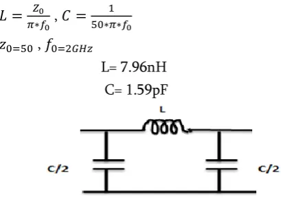
Low pass filters are used in a wide number of applications, mainly used in radio frequency applications [12]. Low pass filters can be made of either RC or LC. Typically they are used to filter out undesired signals that may be present in a band above the wanted pass band. Filter accepts signals below the cut-off frequency. Here, designed low pass filters using LC components inductors and capacitors which can be arranged in either a pi type or T type network. Because of the combination of filtering devices, the ability of the pi filter to remove ripple voltage is superior to that of either the capacitance or inductance filter. Filter determines powerful characteristics of PLL which specify capture range, tracking range [13]. Filter receives signal from phase detector and filters accordingly. After amplifying, output of low pass filter is given as an input to VCO. The proposed PLL was designed for 2GHz frequency, in order to that we need to choose inductor and capacitor value for pi-type filter to eliminate the noisy signal as well as to lock PLL to 2GHz. Calculate inductor and capacitor value, using the formula,
,
,
L= 7.96nH C= 1.59pF
Figure 3. Design of pi-filter
Based on the application we can design the filter using the above formula. Pi filter are used in communication devices for retrieving the particular signal after modulation [14]. In transmission, the signals modulated into multiples of high frequency. While on the receiver side, filters are used to demodulate the particular range of frequency.
IV.
VOLTAGE CONTROLLED OSCILLATOR
A voltage controlled oscillator (VCO) is one of the important basic building blocks in analog and digital circuits. VCO is the main building block in phase locked loop (PLL) and clock generator circuits [8]. There are so many different implementations of VCO’s. One of them is the ring oscillator based VCO, which is commonly used in the clock generation[9].
Figure 4. Deisgn of Ring Oscillator.
International Journal of Scientific Research in Science and Technology (www.ijsrst.com)
1133
V.
FREQUENCY DIVIDER
Frequency divider which is also a clock divider used in the phase locked loop feedback loop, in order to divide the frequency by factor of two. By placing divider in the feedback allow the generation of frequencies based on a stable reference frequency.
Figure 6. Frequency divider circuit
Figure 7. Frequency divider input and output frequency
VI.
SIMULATION RESULTS
The simulation and results of each blocks of PLL is shown below. Those blocks were simulated using Cadence tool in 180nm technology. The proposed system is designed for 2MHz, in that frequency the PLL get locked.
A. Phase Frequency Detector schematic
Figure-8 Phase frequency detector Schematic
B. Simulation Result of PFD
Figure-9 Simulation result of Phase Frequency Detector
1134
Figure-10 Schematic of pi-filter
B. Frequency response curve
Figure-11 Frequency response curve of pi-filter
C. Simulation result of filter
Figure-12 Simulation result of filter
Figure-13 Schematic of VCO
B. Simulation Result of VCO
Figure-14 Simulation result of VCO
A. Frequency divider Schematic
International Journal of Scientific Research in Science and Technology (www.ijsrst.com)
1135
B. Simulation Result of Frequency Divider
Figure-16 Simulation result of frequency divider
A. Schematic of PLL
Figure-17 Schematic of PLL
B. Simulation Result of PLL
Figure-18 Simulation result of PLL
These are the schematics and simulation result of various blocks of Phase Locked Loop which was
implemented and simulated and also results were taken using the Cadence Tool 180nm technology.
VII.
CONCLUSION
In this paper, designed and simulated the various components of Phase Locked Loop using Cadence tool in 180nm CMOS technology. The proposed PLL reveal the behavior of each components of PLL. PLL was designed with a frequency of about 2MHz, which were widely employed in the telecommunication, radio to select the desired frequency channel and also used in the transceiver circuit.
VIII.
REFERENCES
[1]. B. Razavi, Design of Analog CMOS Integrated Circuits, McGraw-Hill, 2001.
[2]. R. Best, Phase-Locked Loops , McGraw-Hill, 1993.
[3]. Phase-locked Loop
http://en.wikipedia.org/wiki/Phase locked loop [4]. Ron Bertrand VK, The Basics of PLL Frequency
Synthesis, ©2002 (online radio electronics course)
[5]. Mark Curtain and Paul O’Brien, Phase-locked loop for high frequency receivers and transmitters part 1, ©1999 33-3 1999 Analogue Dialogue .
[6]. R.E Best, Phase-Locked Loops, Design, Simulation, and Applications, © 2003 5thEdition, McGraw-Hill Publishers.
[7]. Keliu Shu and S-S Edgar, CMOS-PLL Synthesizers, Analysis and Design, Springer Publishers, Boston , © 2005
[8]. A.Rezayee and K.Martin. A three-stage coupled ring oscillator with quadrature outputs. In Proceedings of Int. Symp. on Circuits and Systems., IEEE, 2001.
1136
Range and Fast Voltage Swing, Tokyo Institute of Technology 2-12-1 Oookayama, MeguroTokyo, Japan.
[10]. A.Hajimiri and T.H.Lee. The Design of Low Noise Oscillators. Kluwer Academic Publishers, 1999
[11]. A.Rezayee and K.Martin. A three-stage coupled ringoscillator with quadrature outputs. In Proceedings of Int. Symp. on Circuits and Systems. IEEE, 2001
[12]. Mr. Yeshwanth.A, Mrs. Raji.C, Design of Low power, Dead zone free CMOS PFD for PLL, International Journal of Engineering Research Volume No.5 Issue: Special 5, pp: 992- 1128, 20 May 2016
[13]. Atul S.Joshi, Chaitali P.Charjan Phase Locked Loop using VLSI Technology For Wireless Communication, International Journal Of Innovative Research In Electrical, Electronics, Instrumentation And Control Engineering Vol. 2, Issue 4, April 2014.