University of Massachusetts Amherst University of Massachusetts Amherst
ScholarWorks@UMass Amherst
ScholarWorks@UMass Amherst
Doctoral Dissertations Dissertations and Theses
November 2017
Formal Analysis of Arithmetic Circuits using Computer Algebra -
Formal Analysis of Arithmetic Circuits using Computer Algebra -
Verification, Abstraction and Reverse Engineering
Verification, Abstraction and Reverse Engineering
CUNXI YUECE, University of Massachusetts Amherst
Follow this and additional works at: https://scholarworks.umass.edu/dissertations_2
Part of the Computer Engineering Commons, and the VLSI and Circuits, Embedded and Hardware Systems Commons
Recommended Citation Recommended Citation
YU, CUNXI, "Formal Analysis of Arithmetic Circuits using Computer Algebra - Verification, Abstraction and Reverse Engineering" (2017). Doctoral Dissertations. 1142.
https://scholarworks.umass.edu/dissertations_2/1142
This Open Access Dissertation is brought to you for free and open access by the Dissertations and Theses at ScholarWorks@UMass Amherst. It has been accepted for inclusion in Doctoral Dissertations by an authorized administrator of ScholarWorks@UMass Amherst. For more information, please contact
FORMAL ANALYSIS OF ARITHMETIC CIRCUITS
USING COMPUTER ALGEBRA
- VERIFICATION, ABSTRACTION AND REVERSE ENGINEERING
A Dissertation Presented by
CUNXI YU
Submitted to the Graduate School of the
University of Massachusetts Amherst in partial fulfillment of the requirements for the degree of
DOCTOR OF PHILOSOPHY September 2017
c
Copyright by Cunxi Yu 2017 All Rights Reserved
FORMAL ANALYSIS OF ARITHMETIC CIRCUITS
USING COMPUTER ALGEBRA
- VERIFICATION, ABSTRACTION AND REVERSE ENGINEERING
A Dissertation Presented by
CUNXI YU
Approved as to style and content by:
Maciej Ciesielski, Chair
George S. Avrunin, Member
Daniel Holcomb, Member
Sandip Kundu, Member
Christopher V. Hollot, Department Head Electrical and Computer Engineering
ABSTRACT
FORMAL ANALYSIS OF ARITHMETIC CIRCUITS
USING COMPUTER ALGEBRA
- VERIFICATION, ABSTRACTION AND REVERSE ENGINEERING
SEPTEMBER 2017 CUNXI YU
B.Sc., ZHEJIANG UNIVERSITY CITY COLLEGE Ph.D., UNIVERSITY OF MASSACHUSETTS AMHERST
Directed by: Professor Maciej Ciesielski
Despite a considerable progress in verification and abstraction of random and control logic, advances in formal verification of arithmetic designs have been lagging. This can be attributed mostly to the difficulty in an efficient modeling of arithmetic circuits and datapaths without resorting to computationally expensive Boolean meth-ods, such as Binary Decision Diagrams (BDDs) and Boolean Satisfiability (SAT), that require, bit-blasting, i.e., flattening the design to a bit-level netlist. Approaches that rely on computer algebra and Satisfiability Modulo Theories (SMT) methods are ei-ther too abstract to handle the bit-level nature of arithmetic designs or require solving computationally expensive decision or satisfiability problems.
The work proposed in this thesis aims at overcoming the limitations of analyz-ing arithmetic circuits, specifically at the post-synthesized phase. It addresses the
an algebraic level, treating an arithmetic circuit and its specification as a properly constructed algebraic system. The proposed technique solves these problems by func-tion extracfunc-tion, i.e., by deriving arithmetic funcfunc-tion computed by the circuit from its low-level circuit implementation using computer algebraic rewriting technique. The proposed techniques work on large integer arithmetic circuits and finite field arith-metic circuits, up to 512-bit wide containing millions of logic gates.
TABLE OF CONTENTS
Page
ABSTRACT. . . .iv
LIST OF TABLES. . . x
LIST OF FIGURES. . . xii
CHAPTER 1. INTRODUCTION . . . 1 1.1 Hardware Verification . . . 3 1.2 Verification Techniques . . . 5 1.2.1 Equivalence Checking . . . 5 1.2.2 Model Checking . . . 8 1.2.3 Theorem Proving . . . 8 1.2.4 Symbolic Simulation . . . 9 1.2.5 Reverse Engineering . . . 10
1.2.6 Overview of the thesis . . . 12
2. BACKGROUND . . . 13
2.1 Canonical Diagrams . . . 13
2.2 SAT and SMT solvers . . . 14
2.3 Structural Minimization . . . 18
2.4 Computer Algebra Approaches . . . 19
3. FORMAL VERIFICATION OF INTEGER ARITHMETIC CIRCUITS USING FUNCTION EXTRACTION . . . 25
3.1 Introduction . . . 25
3.2 Function Extraction . . . 25
3.2.1 Algebraic Model . . . 26
3.2.3 Function extraction vs. Polynomial Division . . . 36
3.2.4 Properties of Computed Input Signature . . . 39
3.3 Experimental Results . . . 41
3.3.1 Comparison with SAT and SMT . . . 41
3.3.1.1 SAT comparison: . . . 42
3.3.1.2 SMT experiments . . . 44
3.3.2 Limitations and Proposed Solutions . . . 45
3.3.2.1 Circuit Boundaries . . . 45
3.3.2.2 Output Encoding . . . 46
3.3.2.3 Effects of Synthesis on Function Extraction . . . 47
3.4 Verification of Datapaths - A Case Study . . . 47
3.4.1 Word-level Verification . . . 50
3.4.2 Bit-level Verification . . . 54
3.4.3 Results . . . 55
3.5 Conclusions . . . 56
4. COMPUTER ALGEBRA BASED VERIFICATION WITH REDUNDANT POLYNOMIALS. . . 59 4.1 Introduction . . . 59 4.2 Previous Work . . . 60 4.3 Preliminaries . . . 61 4.3.1 Vanishing Polynomials . . . 63 4.3.2 Don’t-care Polynomials . . . 65 4.4 Sequential Verification . . . 67 4.4.1 Multiply-Accumulator (MAC) . . . 67 4.4.2 Serial Squarer . . . 69 4.5 Experimental Results . . . 71 4.6 Conclusions . . . 73
5. ADVANCED ALGEBRAIC REWRITING USING AND-INV-GRAPH. . . 75
5.1 Introduction . . . 75
5.2.1 Boolean Network . . . 76
5.2.2 Simplified Polynomial Construction . . . 78
5.3 Approach . . . 79
5.3.1 Outline of the Approach . . . 80
5.3.2 Detecting Redundant Polynomials . . . 82
5.4 Results . . . 84
5.5 Conclusion . . . 86
6. ALGEBRAIC SPECTRUM - A NEW CANONICAL REPRESENTATION OF ARITHMETIC . . . 87
6.1 Introduction . . . 87
6.2 Related Work . . . 89
6.3 Algebraic Spectrum . . . 93
6.3.1 Uniqueness of Algebraic Spectrum . . . 94
6.3.2 Example - Single Spectrum Function . . . 97
6.3.3 Example - Multiple-Spectrum Function . . . 99
6.4 Polynomial-Time Spectrum Extraction . . . 100
6.5 Results . . . 104
6.6 Conclusion . . . 106
7. FORMAL ANALYSIS OF FINITE FIELD ARITHMETIC CIRCUITS . . . 107
7.1 Introduction . . . 107
7.2 Background . . . 109
7.2.1 Galois Field Multiplication . . . 109
7.2.2 Irreducible Polynomials . . . 110
7.3 Parallel Extraction in Galois Field . . . 112
7.3.1 Computer Algebraic model . . . 113
7.3.2 Outline of the Approach . . . 113
7.3.3 Implementation . . . 117
7.4 Reverse Engineering in Galois Field . . . 120
7.4.1 Output encoding determination . . . 121
7.4.2 Input encoding determination . . . 122
7.5 Results . . . 127
7.5.1 Parallel Verification of GF(2m) Multipliers . . . 127
7.5.1.1 Design and Verification cost depend on P(x) . . . 129
7.5.1.2 Runtime vs. Memory of Parallelism . . . 130
7.5.1.3 Effect of synthesis on verification of GF(2m) multipliers . . . 131
7.5.2 Reverse Engineering of GF(2m) Multipliers . . . 132
7.6 Conclusion . . . 134
LIST OF TABLES
Table Page
3.1 2-bit multiplier intermedia expression size of two substitution
sequence . . . 30 3.2 N1, N2 are the numbers of nodes before and after f raig -v inABC;
N3, N4 are the numbers of clauses before and after simplification
by [12] . . . 43 3.3 CPU time and memory results of 256-bit (Operands A and B)
arithmetic circuits. (TO = timeout after 3600 sec; MO = memory out of 8 GB). . . 45 3.4 Results for a synthesized multiplier; comparison with [32], SAT,
SMT, and commercial tools (TO = timeout after 3600 sec; UD = undecided; MO = memory out of 8 GB). *ABC was unable to
synthesize the 512-bit CSA multiplier due to memory limit. . . 45 3.5 CPU time and memory results using TDS and Function
Extraction . . . 56 4.1 Verification results for GF(2256) Adder, MAC, and Add-shift
Multipliers . . . 71 4.2 Effect of Vanishing and Don’t Care Polynomials for MAC (MO =
Memory out of 8 GB) . . . 72 4.3 Effect of Vanishing and Don’t Care Polynomials for Serial Squarer
(MO = Memory out of 8 GB) . . . 72 4.4 Sequential Squarer results: comparison with SAT and SMT (TO =
Time out after 3600 sec) . . . 72 5.1 Results of applying AIG-based algebraic rewriting to pre- and
post-synthesized CSA multipliers compared to functional
extraction presented in Chapter 3. *t(s) is the runtime in seconds.
5.2 Results of applying AIG-based algebraic rewriting to post-synthesized complex arithmetic circuits compared to functional extraction
presented in Chapter 3. *MO = Memory out of 8 GB. . . 85 6.1 Results of extracting the specification of pre- and post-synthesized
CSA multipliers compared to functional extraction presented in [31]. *t(s) is the runtime in seconds. *mem is the memory usage
in mb. . . 103 6.2 Results of extracting the specification of the post-synthesized
complex arithmetic circuits compared to functional extraction
presented in [31]. *MO = Memory out of 8 GB. . . 104 6.3 Runtime of extracting the specification of the radix-4 Booth
multiplier. *MO = Memory out of 8GB. . . 104 6.4 Evaluation of word-level abstraction using algebraic spectrum.
Multiplications in F1 and F2 are implemented using
CSA-multiplier. F3 uses radix-4 Booth-multiplier. . . 105
7.1 Results of verifying Mastrovito multipliers using our parallel approach. T is the number of threads. M O=Memory out of 32 GB. T O=Time out of 12 hours. (*T=1 shows the maximum
memory usage of a single thread.) . . . 126 7.2 Results of verifying Montgomery multipliers using our parallel
approach. T is the number of threads. T O=Time out of 12 hours.
M O=Memory out of 32 GB. (*T=1 shows the maximum memory usage of a single thread.) . . . 126 7.3 Runtime and memory usage of synthesizedMastrovito and
Montgomery multipliers (T=20). . . 132 7.4 Results of reverse engineering synthesized and technology mapped
LIST OF FIGURES
Figure Page
1.1 Typical industrial IC design flow. . . 3 1.2 Combinational equivalence checking model. . . 5 1.3 Sequential equivalence checking model. . . 6 1.4 A gate-level circuit implementing 2-input AND function with inputs
a and b. . . 9 1.5 Proving the function of output z in Figure 1.4 is AND(a,b) using
theorem proving. . . 10 2.1 Canonical diagrams - Ordered Binary Decision Diagrams (OBDD); a)
Gate-level design with output z; b) Gate-level design with output
z′
. c) The truth table of z and z′
; d) BDDs of z and z′ are
identical with same variable order. . . 14 2.2 Reduced ordered binary decision diagrams of 4-bit multiplication. . . 15 2.3 Example of equivalence checking using SAT solver using a Boolean
miter. . . 16 2.4 Half adder design with inputa and b. s is the sum function and cis
the carry function. . . 18 2.5 Example of logic minimization. a) Original circuit; b) Circuit with
gates B and C are merged; c) Circuit with gates A and D are
merged. . . 19 3.1 Verifying a 2-bit signed multiplier: Gate-level circuit with output
signature Sigout =−8z3+ 4z2+ 2z1+z0. . . 28
3.2 Two substitution orders for an unsigned 2-bit multiplier. . . 30 3.3 Substitution order analysis using 4-bit, 6-bit, and 8-bit multiplier.
3.4 Parallel prefix adder, hybrid model . . . 34
3.5 Expanding complex gates for cut rewriting. . . 35
3.6 Proof that x5x8 evaluates to 0 using both, the computer algebraic and Boolean methods. . . 36
3.7 2-bit gate-level adder. R =r0+ 2r1+ 4r2, A= a0+ 2a1,B =b0 +b1. R = A+B. . . 37
3.8 Arithmetic function of a 2-bit multiplier extracted from the circuit using TED in normal factored form: Sigin = (−2a1+a0)(−2b1+b0). . . 39
3.9 Verifying combinational arithmetic circuits: CPU time. . . 44
3.10 Verifying combinational arithmetic circuits: Memory usage. . . 45
3.11 Comparing rewriting of the expression Sigout vs individual output bits for a 4-bit multiplier. . . 48
3.12 Synthesis impacts on function extraction . . . 48
3.13 Integer ALU - initial RTL design . . . 49
3.14 Integer ALU - final RTL design . . . 50
3.15 TED representation: (a) word-level model; (b) bit-level model . . . 52
3.16 Modeling of the word-level xor. . . 54
4.1 Sequential n-bit adder, Z =A+B. . . 60
4.2 2-bit combinational squarer circuit. a) Gate-level netlist; b) arithmetic squaring structure. . . 64
4.3 Compare the size of internal expressions with, without don’t care polynomial x3. . . 66
4.4 Original MAC circuit: R=P iAi·Bi+C0. . . 67
4.5 MAC circuit unrolled over two cycles. . . 68
4.7 Unrolled 4-bit Serial Squarer. . . 70 4.8 Evaluation of Don’t Care and Vanishing polynomials on a 4-bit serial
squarer. . . 70 5.1 Representing circuits as AIGs. a) Post-synthesized XOR3 gate-level
netlist. b) AIG of the synthesized XOR3 gate-level netlist. (c) The extracted two XOR2 functions (nodes 6 and 9) and one
XOR3 function (node 9). . . 77 5.2 (a) AIG representation of a post-synthesized 2-bit multiplier
gate-level netlist; (b) The AIG of the 2-bit multiplier shown in Figure 5.2(a); (c) Detected unobserved functions from the AIG
and the correspondences to AIG nodes. . . 79 5.3 Detecting{MAJ3-XOR3} pairs of a 3-bit post-synthesized
CSA-multiplier with MSB z5 deleted. . . 84
6.1 The spectra of 2-bit, 3-bit, 4-bit and 5-bit two-operand
multiplication. . . 96 6.2 Spectra of a 3-bit Booth-multiplier and CSA-multiplier of the four
recorded expressions. . . 97 6.3 Spectra of a 2-bit MAC of the four recorded expressions. . . 98 6.4 Spectra of F1=A×(B+C), F2=A×B+A×C, and F3=A×B. A,B,
and C are 3-bit unsigned words. . . 100 6.5 Extracting the function of 2-bit multiplier using spectral method
without algebraic rewriting. . . 102
7.1 Two multiplications in GF(24) constructed using P(x)1=x4+x3+ 1 and
P(x)2=x4+x+ 1. . . 111
7.2 Extracted algebraic expressions of the four output bits of a GF(24)
multiplier. P(x)=x4+x+1. . . 111
7.3 The gate-level netlist of post-synthesized and mapped 2-bit multiplier over GF(22). The irreducible polynomial P(x) =x2+x+ 1. . . 115
7.4 Function extraction of a 2-bitGF multiplier shown in Figure 7.3
using backward rewiring from PO to PI. . . 116 7.5 Overview of the parallel extraction framework. . . 117
7.6 Step3: parallel extraction of a GF(2m) multiplier with number of
threadsT. . . 118
7.7 Extracting the algebraic expression ofz0 and z1 separately in Figure
7.4. . . 120 7.8 Runtime and memory usage of our parallel verification approach as a
function of number of threads T. . . 130
7.9 Sing thread runtime analysis using Mastrovito multipliers. . . 131
7.10 Result of reverse engineering GF(2233) Mastrovito multipliers that are
implemented using different P(x).. . . 134
7.11 Evaluation of the design cost using GF(2233) Mastrovito multipliers with
CHAPTER 1
INTRODUCTION
With an almost unmanageable increase in the size and complexity of ICs and SoCs, hardware design analysis has become a dominating factor of the overall design flow [44]. Hardware verification is one of the essential procedures in the design flow that checks whether the actual hardware implementation has the correct specification. Specifically, verifying arithmetic computation units are particularly difficult due to the “bit blasting“ issue, i.e., flattening the design specification into to a bit-level. The importance of arithmetic verification problem grows with an increased use of arithmetic modules in embedded systems to perform computation-intensive tasks for multimedia, signal processing, and cryptography applications.
Formal verification techniques can benefit greatly from abstractions of the func-tionality of the circuits being verified. Abstraction reduces the complexity of analysis of the design and may provide a hierarchical view of theregister transfer level (RTL), which could be applied to system-level verification. Word-level abstraction specifi-cally focuses on extracting a word-level representation of the function implemented by a gate-level design. For example, for ann-bit gate-level multiplier, the word-level function can be extracted as Z = AB. We can see that as the datapath size of the multiplier grows, the bit-level representation increases exponentially, while the word-level abstraction does not change. However, formal techniques for abstraction in gate-level design are challenging. The abstraction problems are even harder than the verification problem since there are no clear boundaries of the arithmetic functions in the design.
This thesis aims at overcoming the limitations of analyzing large arithmetic cir-cuits, especially of the post-synthesized circuits. The approach proposed here ad-dresses the verification, abstraction and reverse engineering problems in the alge-braic domain, in which both the implementation and the specification of the arith-metic circuit are represented as pseudo-Boolean polynomials in respective variables (circuit signals). It solves the verification problem by extracting an arithmetic func-tion computed by the circuit directly from its gate-level circuit implementafunc-tion using
computer algebraic methods, called function extraction or algebraic rewriting. This rewriting technique transforms the polynomial representing an encoding of the pri-mary outputs (called the output signature) into a polynomial at the primary inputs (called the input signature). The computed arithmetic function can be used to verify the circuit against the given specification (i.e., the expected function of the design), or to decipher the function performed by the circuit. In the case of an incorrectly implemented function, this method will generate a counterexample (bug trace).
Regarding abstraction, a new canonical representation of arithmetic functions, called algebraic spectrum, is introduced in this thesis. Algebraic spectrum refers the coefficient distribution of the polynomial expressions that are computed using the rewriting technique. We prove that the coefficients distribution of arithmetic function is unique depending on the arithmetic operations. Finally, the verification and reverse engineering problems of Finite Field Arithmetic circuits are explored. For the finite field arithmetics, the main contributions include:
• 1) computer algebraic method is approved to be applied for parallel verification over GF(2m).
• 2) the approach of analyzing the irreducible polynomials of finite field arithmetic is proposed.
Figure 1.1: Typical industrial IC design flow.
• 3) the complete reverse engineering framework of finite field arithmetic is de-veloped.
1.1
Hardware Verification
The importance and difficulty of arithmetic circuit verification can be illustrated by the famousF DIV bug in Intel’s Pentium processor in 1995, which cost Intel $475 million. This bug was not covered by the one trillion simulation vectors used for this processor [27]. Verification is a critical problem in the chip industry since the cost of hardware verification is claimed to be 70 percent of the overall hardware design effort. Although the engineers and researchers invest a lot in hardware verification, it is still challenging as the design complexity increases. The recent verification industry study presented by Foster [44] showed that the average verification time in the last ten years is around 60% (57% in 2014) over the entire chip design period. In this survey, it also shows that there are more than 50% designs requires more than 60% project time in verification only. Most of those designs contain large arithmetic units.
Hardware verification is a process of checking the correctness of the fabricated hardware compared to the specification. However, it is impossible to directly check if the fabricated hardware matches the original specification. Typically, hardware
verification is conducted step-by-step during the design flow. Hence, there are many hardware verification techniques developed that apply on different representations of hardwares, such as verification of HDL, gate-level netlist, schematic netlist, and so on. The design flow typically starts with a high-level specification using hardware description language (HDL) or C/C++. This specification is then compiled into a register-transfer-level (RTL) description, which is further optimized by high-level synthesis and logic synthesis techniques and translated into a corresponding netlist representation. The logic-level netlist is then translated to a physical layout during placement and routing synthesis.
Typically, equivalence checking has been applied at each step to check the equiv-alence before and after each optimization or transformation step in the design flow. There are many verification techniques that apply to different representations of hardware, such as HDL code, gate-level netlist, layout, etc. This thesis focuses on gate-level implementation of arithmetic circuits. Traditional approaches to verifying arithmetic circuits are based on simulation or emulation, but exhaustive simulation is not applicable to the large modern designs. Theorem proving approaches require verification experts to manually guide the systems to complete the proof. Thus, to automatically verify arithmetic circuits, many formal techniques have been developed to handle large practical circuits. However, few formal techniques are applicable to large gate-level arithmetic circuits. Those contemporary formal methods that could be applied to arithmetic circuits verification are reviewed in Chapter 2. The limi-tations of those formal methods for verifying arithmetic circuits are studied in the Chapter 3.
1.2
Verification Techniques
1.2.1 Equivalence CheckingIn recent years, many CAD vendors have offered equivalence checking tools for design verification. Equivalence checking (EC) is one of the most widely used formal techniques in the verification of digital circuits. Depending on the type of the target circuits, i.e. sequential circuits or combinational circuits, equivalence checking can be classified in two types: sequential equivalence checking (SEC) and combinational equivalence checking (CEC).
Inputs
Design 1
Design 2
Figure 1.2: Combinational equivalence checking model.
The Combinational Equivalence Checking (CEC) model is shown in Figure 1.2. Let Design1 be the design to be verified, and Design2 be the reference design. The specification of the reference design is the expected specification of Design1. Given identical inputs toDesign1 and Design2, amiter is built by XORing the correspond-ing output bits of these two designs and connectcorrespond-ing to a wide OR gate. If the functions represented by the two designs are identical for all input patterns, thenmiter always evaluates to 0 (Boolean false) for any input pattern. In this case, the two designs are proved to be equivalent. Otherwise, these two designs are not equivalent.
The Sequential Equivalence Checking (SEC) model is shown in Figure 1.3. SEC checks if the corresponding outputs are equivalent for any state of the two circuits with identical initial states. The proof of correctness of two sequential circuits re-quires a complete state-space traversal, which is one of the bottlenecks of sequential
Inputs
Design 1
Design 2
Sequential States
=? =?
Figure 1.3: Sequential equivalence checking model.
equivalence checking. The complexity of sequential equivalence checking could be significantly increased by synthesis process, such as retiming technique [120].
The most straightforward technique to prove or disprove the equivalence using EC model is exhaustive simulation. It is obvious that exhaust simulation is not pos-sible for design with a large number of input bits. And, random simulation does not provide complete proof of the equivalence because of the coverage problem. Further, formal verification methods are heavily investigated to address the equivalence check-ing problem. The most promischeck-ing formal techniques for solvcheck-ing equivalence checkcheck-ing problem include canonical diagrams, satisfiability and computer algebra methods.
Reduced Ordered Binary Decision Diagrams (OBDDs) [20], provide the efficient method for equivalence checking for combinational and sequential circuits [5]. OB-DDs are canonical representation with a fixed variable ordering. Hence, equivalence checking problem can be addressed by comparing the OBDDs of two designs. If two OBDDs are identical, two designs are functional equivalent. However, the size of the BDDs explodes for large designs. Specifically, it becomes large for the arithmetic circuits. For example, for integer multiplication, it has been shown that an n-bit multiplication requires a O(n3) size OBDD [24].
Due to the limitation of the BDDs, many techniques have been developed to reduce the complexity of equivalence checking. Goldberg et. al [47] presented a simple
framework for SAT-based CEC and reported results on an ISCAS-85 benchmarks. Paruthi et. al [88] proposed an idea that is based on a tight integration of a structural satisfiability (SAT) solver, BDD sweeping, and random simulation. In this work, the integral application of the SAT solver significantly enhances the capacity and efficiency of BDD sweeping and extends its suitability for mis-comparing designs. Further, the random simulation algorithm works on the graph that represents the netlist and thus runs more efficiently. Mishchenko et. al [76] presented an And-Inv-Graph (AIG) data structure that is the state-of-the-art technique for logic reduction and synthesis. TheFunctional-reduced AIG (FRAIG) is able to efficiently reduced the logic complexity [78] which has been implemented in the ABC system [80]. However, all these techniques are not applicable to large arithmetic circuits, such as Galois field multipliers and integer multipliers [31][72].
With significant research efforts spent on formal methods, formal verification for hardware that combines heuristic methods, such as checking structure similarity, be-comes more and more popular. The similarity between the two circuits is exploited to identify the equivalences between internal nodes of the two circuits being checked for equivalence [63]. For example, the partial list of equivalence checkers are Formal-ity (from Synopsys), Design Verifyer (from Chrysalis) and VerFormal-ity (from IBM) [64]. Similarly, identifying structural similarities for sequential equivalence checking is also explored [120]. These tools perform logic equivalence checking of two circuits based structural analysis and BDD techniques. Similarly to other verification techniques, these equivalence checking techniques are limited by the memory explosion problem for arithmetic circuits. Recently, IBM Formal Verification team showed that their tools could automatically verify the floating point division (FDIV) unit using their SixthSense formal engine [62].
1.2.2 Model Checking
Model checking performs verification by exhaustively checking whether a state-transition graph (STGs) satisfies a given property [36]. In this approach, a circuit is described as a state machine with transitions to describe the circuit behavior. The specifications to be checked are described as properties that the machine should or should not satisfy. Model checking is limited by the state-space explosion problem. The state explosion problem refers to the fact that the number of states is exponential in the number of Boolean variables. Explicit state model checkers are based on graph-traversal of the model states, and must keep track of the visited states. However, this is infeasible due to the large size of the modern designs.
BDDs [20] have traditionally been used as a symbolic representation of the sys-tem. Model checkers based on BDDs are usually able to handle systems with hundreds of state variables. However, for larger systems, the BDDs generated during model checking become too large for currently available computers. Also, selecting the right ordering of BDD variables is very important. Boolean Satisfiability (SAT) also oper-ates on Boolean expressions but does not use canonical forms. Biere et. al proposed a SAT procedures for symbolic model checking instead of BDDs [14][13]. They do not suffer from potential space explosion of BDDs and can handle propositional sat-isfiability problems with thousands of variables.
The symbolic model checking can be applied to sequential circuit verification [34]. However, due to the large size of arithmetic circuits, this technique is difficult to check the properties. Additionally, the symbolic model checking has been applied mostly to verifying the properties of systems instead of gate-level implementations.
1.2.3 Theorem Proving
Another class of solvers includes Theorem Provers, deductive systems for proving that an implementation satisfies the specification, using mathematical reasoning. The
proof system is based on a large and strongly problem-specific database of axioms and inference rules, such as simplification, rewriting, induction, etc. Some of the most popular theorem proving systems are: HOL [48], PVS [84], Boyer-Moore/ACL2 [19], and Nqthm [48][56]. These systems are characterized by high abstraction and pow-erful logic expressiveness, but they are highly interactive, require domain knowledge, extensive user guidance, and expertise for efficient use. The success of verification using theorem prover depends on the set of available axioms and rewrite rules, and on the choice and order in which the rules are applied during the proof process, with no guarantee for a conclusive answer. Similarly, term rewriting techniques, such as [121] or [55], are incomplete and “may fail to generate the proof because additional lemmas are needed” [55]. Additionally, theorem proving for gate-level circuits is extremely complex.
a
b z
i
Figure 1.4: A gate-level circuit implementing 2-input AND function with inputs a
and b.
For example, to prove that the circuit shown in Figure 1.4 is a AND2(a, b) func-tion, theorem proving requires ten steps. The specification of z is Fspec=a∧b. The specification of the circuit is F=∃x.i N AN D(a, b, x)∧N OT(x, z). The equivalence checking problem using theorem proving is: ∀ a, b, z F(a, b, z) → Fspec(a,b,z). The procedure of proving the equivalence between Fspec and F using theorem proving is shown in Figure 1.4.
1.2.4 Symbolic Simulation
Symbolic simulation is a well know technique for simulation and verification of dig-ital circuits and is an extension of conventional digdig-ital simulation, where a simulator evaluates circuit behavior using symbolic Boolean variables to encode a range of
cir-⊢ ∃x. NAND(a,b,i) ∧ NOT(i,z) ⊢NAND(a,b,i) ∧ NOT(i,z) ⊢NAND(a,b,i) ⊢i = ¬(a ∧ b) ⊢NOT(i,z) ⊢z = ¬i ⊢z = ¬(¬(a ∧ b)) ⊢z = (a ∧ b) ⊢AND(a,b,z)
⊢F(a,b,z) = Fspec(a,b,z)
Figure 1.5: Proving the function of outputz in Figure 1.4 is AND(a,b) using theorem proving.
cuit operating conditions [21]. Several symbolic simulation tools were developed after Bryant introduced BDDs [18][9]. Bose et. al presented an automated verification tool of synchronous pipelined circuits, based on symbolic simulation [18]. The problem for this work and symbolic simulation is that the specifications must be expressed as Boolean functions, which can be very complex for some arithmetic circuits.
Compared with model checking, symbolic simulation technique can handle much larger circuits, because this approach can only cover some of the input spaces in each simulation run. However, symbolic simulation cannot be used to completely verify arithmetic circuits such as integer multipliers, field multipliers, etc., because the input spaces of these circuits are very large and the BDDs grow up exponentially for these circuits. An exhaustive simulation to cover the entire input space is almost impossible for large arithmetic circuits.
1.2.5 Reverse Engineering
Significant research effort is spent on reverse engineering for hardware security analysis and verification. Physical-based reverse engineering works can be done by decapsulating the chip using imaging and delayering techniques. Torrance and James show that reverse engineering of a fabricated integrated circuit chips can be very
successful [119]. Li et al. presented an automatic approach that identifies high-level components by matching a set of known components [68], and Subramanyan et al. improve that approach to successfully operate on synthesized gate-level netlist [113]. Several logic encryption techniques have been introduced to protect the ICs against those reverse engineering techniques, such aslogic locking andgate-level camouflaging
[93] [123]. Gate-level camouflaging is a particular camouflaging technique that utilizes the camouflaged standard cells for technology mapping against imaging-based reverse engineering. Each camouflaged cell has several possible logic functions at the imaging level, but only one function is physically implemented [94][65]. Alternatively, logic encryption can be done by introducing new primary inputs as key inputs, as well as additional logic, to the original circuits. The correct output value can be computed only if the users are aware of the correct key values [8] [93] [123].
To evaluate the above mentioned encryption techniques, several reverse engineer-ing techniques have been developed based on fault-analysis and formal methods, such as Boolean Satisfiability [95][112][41][69][131]. Specifically, SAT-based reverse engi-neering techniques have been demonstrated to be a significant threat to logic encryp-tion. Subramanyan et. al [112] presented a decryption algorithm based on satisfiabil-ity checking that selects distinguishable input patterns to rule out the incorrect keys. Regarding the encrypted circuits using camouflaged cells, several oracle-guided SAT-based decamouflaging approaches have been developed, while the true functions of the encrypted circuits are assumed to be unknown [41][69]. The reason why SAT-based reverse engineering techniques are very efficient is that each SAT iteration rules out a significant portion (typically more than 99%) of ′′
wrong guesses′′
. In this thesis, a reverse engineering approach of Galois Field arithmetic circuits based on computer algebraic method is proposed. This approach can extract the function of GF mul-tipliers and the irreducible polynomials used for constructing the finite fields, when the binary encodings of the input and output bits are unknown. This is based on
analyzing the algebraic signatures (expressions) of the output bits of gate-level GF multipliers that is described in Chapter 7.
1.2.6 Overview of the thesis
This thesis is organized as follows:
• In Chapter 2, the formal methods that could be used to address the formal analysis problems of arithmetic circuits are reviewed. It includes the explanation of why the contemporary formal methods are limited by analyzing arithmetic circuits.
• Chapter 3 introduces the function extraction technique. It also includes results of evaluating contemporary formal methods and verification of large arithmetic circuits using function extraction.
• In Chapter 4, verification of sequential arithmetic circuits is addressed. Specif-ically, two redundant polynomials are introduced, vanishing polynomial and don’t care polynomial, that significantly reduce the complexity of algebraic rewriting.
• To address the limitation of applying algebraic rewriting on heavily optimized arithmetic circuits, an algebraic rewriting technique based on And-Inv-Graph (AIG) is presented in Chapter 5. Specifically, this technique normalizes arbi-trary gate-level circuits into a netlist with Boolean gates and HAs/FAs.
• The new canonical representation,algebraic spectrum, is introduced in Chapter 6. Using this representation, the word-level abstraction problem of arithmetic datapath is addressed.
• In Chapter 7, the parallel verification and reverse engineering of finite field arithmetic circuits have been addressed.
CHAPTER 2
BACKGROUND
This chapter reviews the contemporary formal methods including canonical di-agrams, Boolean satisfiability (SAT), satisfiability modulo theories (SMT), and the method used in this thesis, computer algebra approach.
2.1
Canonical Diagrams
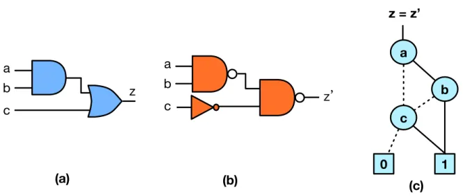
Several approaches have been proposed to check an arithmetic circuit against its functional specification. Different variants of canonical, graph-based representations have been proposed, including Binary Decision Diagrams (BDDs) [20], Binary Mo-ment Diagrams (BMDs) [22] [26], Taylor Expansion Diagrams (TED) [29], and other hybrid diagrams. BDDs are the most extensively used canonical diagrams for syn-thesis and verification. An example of equivalence checking using BDD is shown in Figure 2.2. The Boolean function has been mapped into two different logic designs shown in Figure 2.2 (a) and (b). Since BDD is canonical with a respect fixed variable order, EC can be done by comparing the two BDDs of the two designs with a iden-tical variable ordering. In this example, the variable is orders in a → b → c. If the BDDs are identical, we say the two designs are functional equivalent. Alternatively, equivalence checking can be done by checking if the BDD of a miter can be reduced tozero-BDD.
While BDDs have been used extensively in logic synthesis, their application to verification of arithmetic circuits is limited by the prohibitively high memory require-ment for complex arithmetic circuits, such as multipliers. BDDs are being used, along
a b c z (a) a c b 1 0 z = z’ (c) a b c !" (b)
Figure 2.1: Canonical diagrams - Ordered Binary Decision Diagrams (OBDD); a) Gate-level design with output z; b) Gate-level design with output z′
. c) The truth table of z and z′
; d) BDDs of z and z′
are identical with same variable order.
with many other methods, for local reasoning, but not as monolithic data structure [54]. BMDs and TEDs offer a better space complexity but require word-level infor-mation of the design, which is often not available or is hard to extract from bit-level netlists. While the canonical diagrams have been used extensively in logic synthe-sis, high-level synthesynthe-sis, and verification, their application to verify large arithmetic circuits remains limited by the prohibitively high memory requirement of complex arithmetic circuits [31][128][70]. For example, multiplication is one of the examples that causes memory explosion problem. The BDD of a 4-bit integer multiplication is shown in Figure 2.2, generated using CUDD 2.4.0 package [107]. It includes 1,022 nodes. For a 6-bit multiplication, the number of BDD nodes is 8,176 and increases exponentially with the number of variables.
2.2
SAT and SMT solvers
Arithmetic verification problems can be modeled using Boolean satisfiability (SAT) or satisfiability modulo theories (SMT). Several SAT solvers have been developed to
a3 a2 a1 a0 b0 b3 b2 b1 m0 m1 a0 m2 a1 m3 a2 m4 a3 m5 a3 m6 a3 m7 a3 a3 a2 0 a2 a2 a2 a2 a2 a2 a2 a2 a1 a1 a1 a1 a1 a1 a1 a1 a1 a1 a1 a1 a1 a1 a1 a1 a1 a1 a1 a0 a0 a0 a0 a0 a0 a0 a0 a0 a0 a0 a0 a0 a0 a0 a0 a0 a0 a0 a0 a0 a0 a0 a0 a0 a0 a0 a0 a0 a0 a0 a0 a0 a0 a0 a0 a0 b0 b3 b2 b0 b3 b0 b0 b0 b0 b0 b0 b0 b0 b0 b0 b1 b0 b0 b0 b0 b0 b0 b0 b0 b0 b0 b0 b0 b0 b3 b0 b0 b0 b0 b0 b0 b0 b3 b3 b3 b3 b3 b3 b3 b3 b3 b3 b3 b3 b3 b3 b2 b3 b3 b3 b3 b3 b1 1 b3 b2 b3 b2 b2 b2 b2 b2 b2 b2 b2
Figure 2.2: Reduced ordered binary decision diagrams of 4-bit multiplication.
solve Boolean decision problems, including ABC [75], MiniSAT [109], and others. Some of them, such as CryptoMiniSAT [108], target specificallyxor-rich circuits, but, like all others, are based on a computationally expensive Davis-Putnam-Logemann-Loveland (DPLL) decision procedure. Several techniques combine linear arithmetic constraints with Boolean SAT in a unified algebraic domain [42];
SMT solvers depart from treating the problem in a strictly Boolean domain and integrate different well-defined theories (Boolean logic, bit vectors, integer arithmetic, etc.) into a DPLL-style SAT decision procedure [16]. Some of the most effective SMT solvers, potentially applicable to our problem, are Boolector [82], Z3 [39], and CVC [6]. However, SMT solvers still model the problem as a decision problem and, as demonstrated by our experimental results, are not efficient at solving verification problems that appear in arithmetic circuits.
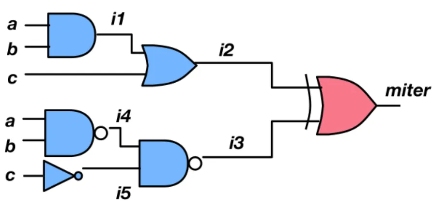
Boolean satisfiability checks if a given problem has a satisfiable solution. In Boolean logic, a formula is in conjunctive normal form (CNF) or clausal normal form which is a conjunction of clauses, where a clause is a disjunction of literals. The SAT solvers take a conjunction of clauses represented in a conjunction normal format (CNF) as input. It produces UNSAT if the problem is unsatisfiable, or produces a solution which satisfies the problem. Equivalence checking using SAT is mostly for-mulated using miter model (Figure 2.3). If the two designs are equivalent,miter will always evaluate to 0 (Boolean false). Hence, if two designs are equivalent, the result
returned by the SAT solver will be UNSAT. An example of a gate-level equivalence checking example using SAT solver is shown in Figure 2.3.
a b c a b c miter i1 i2 i3 i4 i5
Figure 2.3: Example of equivalence checking using SAT solver using a Booleanmiter.
The gate-level model of miter has to be translated into CNF first. The transfor-mation between logic gates to CNF format is shown in Equation 2.1. After converting the model to a CNF, a unit clause (miter) will be added. The meaning of this unit clause is that given the condition thatmiter always evaluates to 1, SAT solvers checks whether there exist a satisfiable solution in this problem. If the result is UNSAT, it means they are equivalent, which means thatmiteralways evaluates to 0. Otherwise, it returns a counterexample and returns Satisfiable. The same formulation can also be solved using SMT solvers. In addition to equivalence checking, this model has been applied to reverse engineering camouflaged circuits and solved by SAT solvers [69][132].
CN F(miter) = (¯a+ ¯b+i1)(a+ ¯i1)(b+ ¯i1)
∧(i1+c+ ¯i2)( ¯i1+i2)(¯c+i2)
∧(¯a+ ¯b+ ¯i4)(a+i4)(b+i4)
∧(¯c+ ¯i5)(c+i+ 5)
∧( ¯i4+ ¯i5+ ¯i3)(i4+i3)(i5+i4)
∧( ¯i2+ ¯i3+miter¯ )(i2+i3+miter¯ )(i2+ ¯i3 +miter)( ¯i2+i3+miter)
∧(miter)
(2.1)
While SMT solvers supportbit-vector operations, they allow formulating the logic in pseudo-Boolean expression. In other words, SMT solvers could solve a satisfiability problem of a word-level miter. For example, to check if a Half-adder (HA) shown in Figure 2.4 is correct, a word-level miter equals to miter=a +b-(2c+s). The formulation for the logic gates is the same as the CNF as shown in the SAT example. Instead of adding a unit clause for the miter, a word-level miter with bit-vector formulation is required in this modeling. The formulation is shown in Equation 2.2. The last equation is the word-level miter. It models the miter as bit-vector adding (a+b) and (−2c−s). In the formulation, 10 is bit-vector constant 2. In Chapter III, I evaluate several state-of-the-art SAT solvers, and SMT solvers with two models, a Boolean model and a word-level model, using arithmetic benchmarks. It shows that these techniques cannot efficiently solve the verification problem of large arithmetic circuits.
a
b c
s Half Adder
Figure 2.4: Half adder design with input a and b. s is the sum function and c is the carry function.
(¯a+ ¯b+ ¯s)(a+b+ ¯s)(a+ ¯b+s)(¯a+b+s)
∧(a+b+ ¯c)(¯a+c)(¯b+c)
∧(bvadd (bvadd(a, b) , ¬bvadd(bvmul(10, c), s)))
(2.2)
2.3
Structural Minimization
Instead of solving the verification problem directly, there are many techniques de-veloped to reduce the size of the problem first. Structural-based logic minimization technique based on logic rewriting on the graphs that describe the circuit structure has been demonstrated to be efficient in reducing the complexity of equivalence checking problem. Mishchenko et. al [76] presented an And-Inv-Graph (AIG) data structure that is the state-of-the-art technique for logic reduction and synthesis. Specifically,
Functionally-reduced AIG (FRAIG) was developed for reducing the logic complexity that combines random simulation, SAT-based equivalence checking, and logic rewrit-ing based on AIG. It is also known as equivalence nodes identification [78].
As an example, consider the circuit includes with AND gates, shown in Figure 2.5(a). First, logic minimization process identifies that the output function of gates B and C are identical (Figure 2.5(b)). Hence, the logic function can be minimized by eliminating the gate C and merging outputz1 with z0. Note that this process aims to
A B C D i1 i2 i3 z0 z1 z2 A B # $ $ $ ( ( ( D i1 i2 i3 z0 z1 z2 B (a) (b) (c)
Figure 2.5: Example of logic minimization. a) Original circuit; b) Circuit with gates B and C are merged; c) Circuit with gates A and D are merged.
is not changed. Similarly, gate A can be eliminated since the output function is the same as gate D (Figure 2.5(c)). Hence, the original function can be represented using two AND functions instead of four AND functions. Assume to use SAT solver, this function is converted to CNF format with only six clauses instead of twelve clauses. However, this technique cannot efficiently reduce the complexity of combinational equivalence checking of non-linear arithmetic circuits. This is demonstrated in Chap-ter III Table 3.2 using a miChap-ter of two gate-level integer multipliers. It shows that the size of the miter is only reduced up to 0.1% using 64-bit or larger multipliers. Similarly technique for reducing the size of the SAT problems is also evaluated in Chapter III Table 3.2.
2.4
Computer Algebra Approaches
One of the most advanced techniques that have potential to solve the arithmetic verification problem are those based on symbolic Computer Algebra [38]. These methods model the arithmetic circuit specification and its hardware implementation as polynomials [96],[103],[122],[89],[71],[91]. The verification goal is to prove that implementation satisfies the specification by performing a series of divisions of the specification polynomial F by the implementation polynomials B = {f1, . . . , fs}, representing components that implement the circuit. For example, the specification
of a multiplier circuit with word-level inputs X, Y and output Z is F =Z −X ·Y. The implementation polynomials are derived from gate equations, similar to those shown later in Equation(7.1).
To systematically perform polynomial division, term ordering “>” is imposed on monomials, so that each polynomial has a well defined leading termlt(). If polynomial
f contains some term t that is divisible by the leading term lt(g) of polynomial
g, then the division of f by g gives a remainder polynomial r = f − t
lt(g) ·g. In
this case, we say that f reduces to r modulo g, denoted f −→g r. With this, the verification problem is posed as the reduction of F modulo B, denoted F −→B + r.
The remainder r has the property that no term in r is divisible by the leading term of any polynomial fi in B. The sign + refers to the fact that the division process is sequential, using polynomials of B one by one. Let B = {f1, ...fs} be a set of polynomials representing circuit elements (logic gates, half adders, etc.) and letRbe a polynomial ring,R =F{x1, ..., xn}. The set of polynomialsB ={f1, . . . , fs}generates
an ideal J = hf1, ..., fsi with fi ∈ Fq, defined as: J = hf1, ..., fsi = h1f1 +...+hsfs
∈Fq. The polynomialsf1, ..., fs are called the bases, orgenerators, of the ideal J. In
the context of circuit verification, they model the implementation of the circuit. In some cases, this test can be simplified to checking iff ∈I(VFq) =J+J0, which
is known in computer algebra as ideal membership testing. While an ideal J may have many different representations, the Grobner Basis of J is unique in order to a monomial order.
A standard procedure to test if F ∈J is to divide polynomial F by f1, ..., fs, one by one. The goal is to cancel, at each iteration, the leading term ofF using one of the leading terms off1, ..., fs. If the remainder of the division isr= 0, thenF vanishes on
V(J), proving that the implementation satisfies the specification. However, if r 6= 0, such a conclusion cannot be made: B may not be sufficient to reduceF to 0, and yet the circuit may be correct. To check ifF is reducible to zero one must use acanonical
set of generators,G={g1, ..., gt}, calledGroebner basis. Without Groebner basis one cannot answer the question whether F ∈J.
Several algorithms have been developed to compute Groebner basis over the field, including the well known Buchberger’s algorithm [23]. However, this algorithm is computationally expensive, as it computes the so-called S-polynomials, by perform-ing expensive division operation on all pairs of polynomials in B. Even with newer algorithms, such as F4 [43], the computational complexity of Groebner basis compu-tation remains prohibitively large for arithmetic circuits. Furthermore, what is the most important, these algorithms do not apply directly to rings over integers, Z2n,
which is needed to solve the verification problem for arithmetic circuits considered in this work. In general, this problem cannot be solved by testing if F is a mem-ber of an ideal J = hf1, ..., fsi, i.e., if F ∈ J. Many of the results related to ideal membership that are valid over algebraically closed fields are fundamentally unsolved over integers Z. It has been shown that solving the problem for Z2n requires testing
if F ∈ I(V(J)), where I(V(J)) is a set of all polynomials that vanish on V(J) [1] [71]. Unfortunately, except for some special cases (such as Galois fields, F2k), it is
not known what I(V(J)) is. Many of the results related to ideal membership that are valid over algebraically closed fields are fundamentally unsolved over integers Z.
Wienand et. al. [122] model an arithmetic circuit as anarithmetic bit-level (ABL) network of adders and other arithmetic operators. Both the specification and the arithmetic operators are represented as polynomials over Z2n. They show that, the
properly ordered setG of polynomials representing logic gates automatically renders it a Groebner basis. The verification problem is solved by testing if specification F
reduced modulo G vanishes over Z2n using a computer algebra system, singular
[40]. In [89], the solution is further restricted to variables in Z2 and the reduction
formulated directly over quotient ring Q=Z2n[X]/hx2−xi. Here, the ideal hx2−xi
elegant, adding this constraint for all variables makes the method computationally expensive for gate-level circuits. For this reason, the method of [89] is limited to ABL networks composed of half adders (ha). Unfortunately, it is not always possible to extract adders from a gate-level circuit, especially in highly bit-optimized implemen-tations. For this reason, this method is not applicable to gate-level implementations, considered in this work.
Kalla, et. al [71][91][92][114], formulated the verification problem similarly, but applied it to Galois field (GF) arithmetic circuits, which enjoy certain simplifying properties. Specifically, for GF, the problem reduces to the ideal membership testing over a larger ideal that includes J0 = hx2 −xi in F2. The solution uses a modified
Gaussian elimination technique. In [91], a symbolic computer algebra method is used to derive a word level abstraction for GF circuits, where GF operators are elements of a polynomial ring with coefficients in F2k. This work relies on the customized
computation of Groebner basis and applies only to GF networks. It does not extend to polynomial rings in integers Z2n which is the subject of this work.
A different approach to arithmetic verification has been proposed in work of Basith et. al. [7] and Ciesielski et. al. [30], where a bit-level network is described by a system of linear equations. The system is then reduced to a single algebraic signature, FSig, using standard linear algebra methods and compared to the specification polynomial
Fspec. A non-zero residual expression, RE = FSig − Fspec, determines a potential mismatch between the implementation and the specification, indicating a potential design error. An additional step is needed to check if RE = 0, which may be as difficult as the original problem itself. Furthermore, this method can only handle networks with linear signatures. An attempt to use a different model [30], by viewing the computation performed by the circuit as a flow of binary data has not offered particular improvement; the issue of testing if RE = 0 was replaced by checking the relation between the fanouts and floating signals that correctly captured the
Boolean nature of circuit variables but still is applicable only to networks with linear input signatures. An extension to this work has been recently presented in [32], by computing input signature from the known output signature using a network-flow approach. This technique also relies on the half-adder (HA) based circuit structure and represents logic gates as elements of has. Logic gates that cannot be mapped into adders are represented a proper combination ofhas, with an unused output left as “floating”. Additional constraint relating floating signals to fanouts in the circuit must be satisfied for the result to be trusted; however, the computation to verify this condition can be expensive. For this reason, this method becomes inefficient if the number of logic gates dominates the ha network. Also, the circuit would need to be partitioned into linear and non-linear portions, which is a non-trivial task.
In contrast, the technique described in this work targets on an arbitrary, unstruc-tured gate-level arithmetic circuit without requiring any reference to higher level models such as adders; it can efficiently handle nonlinear circuits without a need to distinguish between linear and nonlinear parts.
In summary, the problem of formally verifying integer arithmetic circuits over integers Z2n remains open. Currently, there are no known mathematical solutions
to this problem in Z2n. The approaches discussed above that managed to reduce
the verification problem to testing if F ∈ J impose restrictions on the type of the circuits that they can handle [89] [71]. Others, such as [7] cannot properly model the inherently Boolean signals using algebraic models. To the best of our knowledge, the techniques reviewed here cannot efficiently solve the verification problem for gate-level arithmetic circuits in Z2n over Boolean variables Z2, which is the problem in
this work.
The technique proposed here solves the functional verification problem by devising an alternative but equivalent method, based on polynomial substitution and elimina-tion. It correctly implements ideal membership testing without a need for expensive
division process with Groebner basis. The results demonstrate that it scales better and is more efficient than the state-of-the-art computer algebra methods.
CHAPTER 3
FORMAL VERIFICATION OF INTEGER ARITHMETIC
CIRCUITS USING FUNCTION EXTRACTION
3.1
Introduction
The chapter presents an algebraic approach to functional verification of gate-level, integer arithmetic circuits, called function extraction. The arithmetic verification is based on extracting a unique bit-level polynomial function implemented by the circuit, directly from its gate-level implementation. The method can be used to verify the arithmetic function computed by the circuit against its known specification, or to extract the arithmetic function implemented by the circuit. Experiments were performed on arithmetic circuits synthesized and mapped onto standard cells using ABC system. The results demonstrate scalability of the method to large arithmetic circuits, such as multipliers, multiply-accumulate, and other elements of arithmetic datapaths with up to 512-bit operands and over 2 million logic gates. The results show that our approach wins over the state-of-the-art SAT/SMT solvers by several orders of magnitude of CPU time. The procedure has linear runtime and memory complexity, measured by the number of logic gates.
3.2
Function Extraction
Function extraction is done by transforming the polynomial representing the en-coding of the primary outputs (called the output signature) into a polynomial at the primary inputs (the input signature). If the specification of the circuit is known, the extracted input signature will be compared with that specification, and in case
of a mismatch, it will provide a counter-example (bug trace) [46]. Otherwise, the computed signature identifies the arithmetic function implemented by the circuit.
The method uses an algebraic model of the circuit, with logic gates represented by algebraic expressions, while correctly modeling signals as Boolean variables. In contrast to [32], it works directly on unstructured, gate-level implementations. And, in contrast to [89],[91] and other computer algebra methods, it is done using effi-cient polynomial transformation, without a need for expensive Groebner Basis based polynomial division.
To the best of our knowledge, this approach has not been attempted before in the context of gate-level integer arithmetic in Z2n1. It provides a practical method
for checking if the implementation satisfies the specification without resorting to the ideal membership testing in Z2n.
3.2.1 Algebraic Model
The circuit is modeled as a network of logic elements of arbitrary complexity: basic logic gates (and, or, xor, inv) and complex (aoi, oai, etc.) standard cell gates obtained by synthesis and technology mapping. In fact, the proposed model admits a hybrid network, composed of an arbitrary collection of logic gates and bit-level arithmetic components. At one extreme, it can be a purely gate-bit-level circuit; at the other, a network composed of arithmetic components only. Each logic element is modeled as a pseudo-Boolean polynomial fi, with variables from Z2 (binary) and
coefficients fromZ2n (integers modulo 2n). The following algebraic equations are used
to describe basic logic gates:
1
The functional abstraction technique described in [91] applies only to Galois field circuits and is based on polynomial reduction via Groebner basis.
¬a= 1−a a∧b =a·b
a∨b =a+b−a·b
a⊕b =a+b−2a·b
(3.1)
In our model, the arithmetic function computed by the circuit is specified by two polynomials: an input signature and an output signature. The input signature,
Sigin, is a polynomial in primary input variables that uniquely represents the integer function computed by the circuit, i.e., its specification. For example, an n-bit binary adder with inputs {a0,· · · , an−1, b0,· · · , bn−1}, is described by Sigin = Pn
−1 i=0 2
ia i+ Pn−1
i=0 2ibi. Similarly, the input signature of a 2-bit signed multiplier, shown in Fig. 3.1, is Sigin = (−2a1 +a0)(−2b1 +b0) = 4a1b1 −2a0b1 −2a1b0+a0b0, etc. In our
approach, the input specification need not to be known; it will be derived from the circuit implementation as part of the verification process.
Similarly, the output signature, Sigout, of the circuit is defined as a polynomial in the primary output signals. Such a polynomial is uniquely determined by the
n-bit encoding of the output, provided by the designer. For example, the output signature of the 2-bit signed multiplier in Fig. 3.1 is −8z3 + 4z2 + 2z1 + z0. In
general, an output signature of an unsigned arithmetic circuit withn output bitszi is represented as a linear polynomial,Sigout =
Pn−1
i=0 2i zi. Similar expression is derived for signed arithmetic circuits, with its most significant bit zn−1 having a negative coefficient −2n−1
.
Our goal is to transform the output signature, Sigout, using polynomial represen-tation of the internal logic elements, into the input signature,Sigin. By construction, the resulting Sigin will contain only the primary inputs (PI) and will uniquely de-termine the arithmetic function computed by the circuit (cf. Theorem 1 in Section 3.2.4).
a0 b0 a1 b1 x1 x2 x3 x4 x7 F0 F1 F2 F3 F4 F5 F6 F7 x8 z3 z2 z1 z0 x5 x6 x9
Figure 3.1: Verifying a 2-bit signed multiplier: Gate-level circuit with output signa-ture Sigout =−8z3+ 4z2+ 2z1+z0.
3.2.2 Outline of the Approach Algorithm 1 Verification Flow
Input: Gate-level netlist, output signature Sigout (input signature Sigin)
Output: P seudo−Booleanexpression extracted by rewriting
1: Parse gate-level netlist; create algebraic equations for gates/modules 2: Find ordering for variable substitution (levelization, dependency)
3: i = 0; Fi = Sigout
4: while there are unused equations do
5: Rewrite: Fi+1 = Fi with variables substituted with gate equations;
6: i = i + 1
7: end while
8: return F = Fi (to be compared with Sigin)
The proposed verification flow is outlined in Algorithm 3. The inputs to the algo-rithm are: the gate-level netlist (implementation); output signature Sigout (encoding of the result at PO); and optionally the input signatureSigin(specification). The first step is to translate the gate-level implementation into algebraic equations (line 1). Then, the algebraic equations are ordered according to the circuit structure and its
topology by algorithms that try to keep the size of the intermediate expressions small (line 2). Specific algorithms (levelization and dependency) are discussed in the next section. The rewriting process is an iterative application of rewriting one pseudo-Boolean expression into another in the predetermined order (lines 3−6), starting with the output signature Sigout at the primary outputs, PO. At each iteration, all variables in the current expression are substituted by the corresponding gate expres-sions. Each iteration produces its own expression, Fi (line 5). The process ends when the rewriting reaches the primary inputs, PI, (line 7), or when all equations have been used. The resulting expressionF can then be compared withSigin, if it was provided by the designer, to determine if the circuit correctly implements the spec-ification. Otherwise, the computed expression F determines the arithmetic function implemented by the circuit.
The rewriting process is illustrated with a simple 2-bit signed multiplier example, shown in Fig. 3.1. Each equation corresponds to a cut in the circuit, i.e., a set of signals that separate primary inputs from primary outputs; its pseudo-Boolean expression is denoted in the Figure by Fi.
First, F0 is transformed into F1 using substitutions z3 = 1−x8 and z2 = 1−x9.
Subsequently, F2 is obtained from F1 using equations for x8 and x9, and so on,
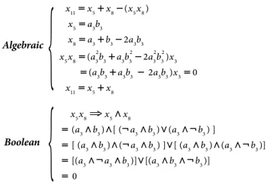
culminating at the primary inputs with expression F7 = 4a1b1−2a0b1−2a1b0+a0b0.
F0 =−8z3+ 4z2+ 2z1+z0 F1 = 8x8−4x9+ 2z1+z0−4 F2 = 8(x1+x7−x1x7)−4(x1+x7−2x1x7) + 2z1+z0−4 F3 = 4x1+ 4x7+ 2z1+z0−4 F4 = 4x1+ 4x5x6+ 2(x5+x6−2x5x6) +z0−4 F5 = 4x1+ 2(x5+x6) +z0−4 F6 = 4x1−2x2−2x3+x4 F7 = 4a1b1−2a0b1−2a1b0+a0b0 = (−2a1+a0)(−2b1+b0)
Note the local increase in the polynomial size (at F2 or F4) known as “fat belly”
effect, before it is eventually reduced to the expression in PIs only. The choice of the cuts and the order in which the variables are eliminated by substitution has a big influence on the size of the fat belly and the efficiency of the method. The following heuristics are used to keep the size of the intermediate expressions as small as possible.
z
3z
2z
1z
0 x 1 x2 x3 x4 x5a
1 b a0 1 b0 6 (a) (b) x 1 x2 x3 x4 x5a
1 b a0 1 b0z
3z
2z
1z
0 7 8 4 5 2 3 1 2 5 1 8 7 6 3 4Figure 3.2: Two substitution orders for an unsigned 2-bit multiplier.
Table 3.1: 2-bit multiplier intermedia expression size of two substitution sequence #.iteration 1 2 3 4 5 6 7 8
Exp. size(a) 4 4 4 6 6 4 4 4 Exp. size(b) 4 4 6 8 6 4 4 4
• Substitution order: The substitution order has the greatest influence on the intermediate expression size (the number of monomials). Even for a small difference between two orders, the maximum intermediate expression size may differ by several orders of magnitude larger in a large design. We illustrate the impact of the substitution order using a 2-bit multiplier (Figure 3.2). Orders (a) and (b) are two different substitution solutions which the first four iterations are different. We record the intermediate expression size step by step during rewriting (TABLE 3.1). We can see that order (b) experiences a larger peak
than order (a). We present two methods to find the efficient substitution order:
Dependency and Levelization.
– Dependency: Substitution must follow the reversed-topological order; once a given variable (output of a gate) is substituted by an algebraic ex-pression of the gate inputs, it will be eliminated from the current exex-pression and will never be considered again. That is, a variable is substituted for only after substituting all signals in its logical cone. For example, in Figure 3.1, before substituting forx6, one must substitute forx7 andz1, since they
both depend on x6. Otherwise, one will be forced to substitute again for
the same variable(s) (in this casex6) again later after substituting the
sig-nals in the cone below. Then, opportunity for early cancellations would be missed, leading to a potential computational explosion. Since the circuit is acyclic, there always exists an ordering of substitutions that satisfies this condition. We refer to this topological constraint informally as “vertical”, since it orders variables upwards from POs to PIs.
– Levelization: To further increase the efficiency of substitution, a ”hori-zontal” constraint is also imposed on the ordering of the candidate variables at a given transformation step. Specifically, the variables that are at the same logic level (from PIs) and have transitive fanin to common variables should be eliminated together, as this will maximize a chance of the re-duction of common terms. It is these variables that define the best cut at each step of the procedure.
We demonstrate why substitution order greatly impacts the rewriting process using larger examples (Figure 3.3). We compare the rewriting process of 4-bit, 6-bit, and 8-bit CSA multipliers using dependency and levelization. In Figure 3.3, the x-axis represents the rewriting process in percentage of computation.
The y-axis represents the size of intermediate expression, i.e. the number of monomials in the expressions. We can see that the difference of the size of the intermediate expression using dependency and levelization increases when the size of the design is increasing. This means that the substitution order has greater impact on the rewriting process if the designs are more complex.
10 100 0 0.1 0.2 0.3 0.4 0.5 0.6 0.7 0.8 0.9 1 #. monomials Rewriting process 4-bit Dep 4-bit Lev 6-bit Dep 6-bit Lev 8-bit Dep 8-bit Lev
Figure 3.3: Substitution order analysis using 4-bit, 6-bit, and 8-bit multiplier. Dep
is dependency; Lev is levelization.
• Fanouts: The size of the intermediate polynomial generated during rewriting can be reduced by identifying variables that depend on common inputs (fanouts of some variables). In this case, the substitution of such variables can be done simultaneously as this increases a chance for eliminating common subexpres-sions. For example, in Fig. 3.1 variables x8, x9 in subexpression (8x8 −4x9)
of F1 depend on common fanout variables x1 and x7. As a result, the
subex-pression (8x8−4x9) = 4(2x8−x9) reduces to 4(x1+x7), without introducing a
terms are particularly harmful if their variables continue to be substituted by other variables, potentially leading to an exponential explosion.
Another simplification that can be applied during rewriting relies on recognizing some pre-defined multiple-input modules with known I/O signatures, such as half adder or full adder. Adders are particularly useful, since they exhibit linear relationship between their inputs and outputs. For example, the circuit in Fig. 3.1 contains a half adder with inputsx5, x6 and outputsx7, z1, with a linear I/O
relationship described by (x5+x6 = 2x7 +z1). In this case, the subexpression
4x7+2z1inF3can be directly translated into 2(x5+x6), avoiding an intermediate
nonlinear term 4x5x6 ofF4. As a result, cutF3 can be directly transformed into
F5.
In order to perform an efficient rewriting, we must analyze circuit topology to find the order will maximize the number of cancellations. The ordering algorithm must recognize reconvergent fanouts that can offer simplification of internal logic. For example, in the parallel prefix adder circuit, Fig. 3.4, both inputs of each or gate are coming as reconvergent fanouts from a half adder. This effectively reduces the algebraic equation for orfroma∨b =a+b−abto justa+b. For example, signals x5 =a3∧b3 and x8 = (a3⊕b3)∧x3 are coming
from thecarry (C) and sum(S) outputs of ha3, so that x5x8 = 0. As a result,
x11 at the output of or1 gate simplifies tox5+x8.
• Vanishing Polynomials: In some arithmetic circuits a particular output bit may always evaluate to zero. This is typically associated with MSB, but this is not the only case. For example, in the squarer circuit (Z =A2) the output bit
z1 is always 0. For this reason one may want to exclude bit z1 from the output
signature,Sigout = Pn−1
i=0 2
i z
i. However, the set of algebraic expressions associ-ated with the term 2z1 offers some early simplification during the computation
FA0 FA1 HA2 HA3 HA4 AND1 AND2 AND3 OR1 OR2 OR3 XOR a0b0c0 a1b1 a2 b2 a3 b3 Cout S3 S2S1 S0 x1 x2 x3 x4 x5 x7 x8 x6 x11 x10 x9 x12
Figure 3.4: Parallel prefix adder, hybrid model
of the signature, before it reaches the primary inputs. Obviously, the logic cone of z1 itself