I
[
[:
[
(
l:
I:
I"
('
[
I
I
I
[
I
[
(
I
I
CIP/2000 COMPUTER
INTERFACE MANUAL
February 1970
Publication 3 501 0108
Price
$
3.00
CINCINNATI
MILACRON
[
[
[
[
[
,I
I
[
[
[
[
[
[J
11
[
[
[
[
~-~~---[
[
[
I
[
1.[,
1.1 1.21.3 1.4
[
1.51.6 1.7 1.8
I
1.91.10 1.11
[
2.2.1
[
2.22.3 2.4
14
3.3.1
r
3.23.3 3.4 3.5
r
3.63.7 3.8 3.9
[
3.103.11 3.12
I"
3.13 3.143.15 3.16
I~
3.173.18 3.19 3.20
(
3.213.22 3.23
I
3.24 3.253.26 3.27
I
I
-TABLE OF CONTENTS
GENERAL INFORMATION . . . .
Introduction . . . . . . . I/O System Organization . . . . Serial I/O Interface . . . . Byte I/O Interface . . . . Program-Controlled I/O . . . . Concurrent I/O . . . . External Priority Interrupts . . . . Direct Memory Interface. . . . Mechanical Considerations . . . . Mainframe Chassis . . . . Expansion Chassis . . . .
SERIAL I/O INTERFACE . . . .
1-1 1-1 1-1 1-3 1-3 1-3 1-3 1-3 1-5 1-5 1-5 1-6 2-1
Introduction . . . 2-1 Character Assembly and Disassembly. . . 2-1 Microcommands and Macro Instructions . . . 2-2 Teletype Interface Connection .. . . . 2-3
BYTE I/O INTERFACES . . . . 3-1
Introduction . . . 3-1 Byte I/O Bus. . . 3-1 Input Data Lines . . . 3-1 Output Data Lines . . . 3-1 Input Control Lines . . . 3-3 Output Control Lines . . . 3-3 Internal Byte I/O Control Lines (Mainframe Chassis) . . . 3-4 External Byte I/o Control Lines (I/O Cable) . . . 3-5 Spare Lines . . . 3-5 Byte I/O Fundamentals . . . 3-5 Device Addressing. . . 3-5 Device Orders. . . 3-5 Status Bytes . . . 3-6 Byte I/O Operations and Timing . . . 3-6 Program-Controlled I/O Operations . . . 3-6 Data Output Timing .. . . . 3-6 Typical Data Output Logic . . . 3-6 Function Output Timing. . . 3-9 " Typical Function Output Logic . . . 3-9 Data Input Timing . . . 3-9 Typical Data Input Logic. . . 3-11 Status Input Timing . . . 3-11 Typical Status Input Logic. . . 3-11 Typical Program-Controlled Transfer Sequence . . . 3-11 Concurrent I/O Operation . . . 3-12 Concurrent I/o Timing. . . 3-14 Typical Concurrent I/o Logic . . . 3-14
---_ .. _-"-. _
-Contents
Contents iv 3.28 3.29 3.30 3.31 4. 4.1 4.2 4.3 4.4 4.5 4.6 4.7 4.8 4.9 4.10 4.11 4.12 4.13
A.
B. C. 1-1 1-2 1-3 1-4 1-5 2-1 2-2 3-1 3-2 3-3 3-4 3-5 3-6 3-7 3-8 3-9 3-10 3-11 3-12 3-13 4-1 4-2 4-3 4:..4 4-5TABLE OF CONTENTS (Cant.)
External Interrupt Operation . . . . Priority Determination . . . ." . . . . Interrupt Requests . . .". . , : . . . • . : . . . . Interrupt Sequence and Timing . . . .
DIRECT MEMORY ACCESS INTERFACE
Introduction . . . . . . . DMA Selector Channels. . . • . . . . DMA External Interface Lines . . . .
Data Output Lines . . . .. Data Input Lines . . . . Device Status Lines . . . . Control Lines . . . . DMA Control . . . .
DMA Channel Operations. . . . . . . Simple Block Transfer . . . . . . . Continuous Block Transfer . . . . . . . Block Transfer with Linked Buffers . . . . Interface to DMA Channel . . . .
APPENDIXES
INTERFACE CONNECTOR SIGNAL LISTS . • . . . . • . . . • . . . • . . • • . • . . . I/O INTERFACE SIGNAL GLOSSARY . • • • . • • • . . . , • • . . . • . • . • • • . • • . . TELETYPE MODIFICATION PROCEDURES • . • . . . . • . . . • . • . • . . . • . .
ILLUSTRATIONS
Typical CIP/2000-Series I/O Configuration .. .
Mainframe Chassis Interface Connectors .. .
Interface Circuit Board Dimensional Data . . . .
I/o
Line Driver and Receiver Interface Option . . . .. I/O Expansion Cabling . . . . SerialI/o
Interface Circuit . . . . Serial I/O Timing . . . . Byte I/O Interface, Simplified Logic Diagram . . . . Relationship of Control Signals CPHI and CPH2/ . . . . Data or Function Output Timing . . . . Data Output Logic . . . • . . . Function Output Storage and Decoding Logic . . . . Data or Status Input Timing . . . . Data Input Logic . . . . Status Input Logic . . . . Typical Program-Controlled Transfer Sequence . . . . Concurrent I/O Timing . . . ; . . . . Concurrent I/O Logic . . . . Typical Priority Wiring Scheme . . . . External Interrupt Timing . . . . Relationship of Processor, Memory, and DMA Channels . . . . DMA Channel Control Word Memory Locations . . . . DMA Channel Block Transfer Timing . . . . DMA Status Byte Format. . . . DMA Bus Cabling for Muitiple Controllers . . . .--_ .. -
----.--[
Contents
[
TABLES
[
1-1 1-23-1
I/O Interface Options . . . • . . . 1-4 I/O Cable Specifications . . . 1-7 I/O Control States . . . 3-4 3-2 Standard I/O Device Addresses . . . 3-6
[
3-3,
3-4 4-1
Standard I/O Device Orders. . . 3-7
I/O Device Status Byte Definition . . . 3-7 DMA Channel Instructions. . . 4-5
[
I
[;
r
[
(i
I'
I
I
[
[
[
I
I
[
[
[
[
1
I
[
I
if
1.
I
1
· :
" "1
[
1
[
~
~
[
[
[
I
I'
I
l
[
(
(
[
1.1 INTRODUCTION
This manual describes the three primary input/output interfaces of the CIP/200o-series computers and pro-vides guidelines for connecting external equipment to the interfaces. The information in this manual should not be considered the final authority for the
Vo
inter-face configuration of any particular machine. The final authority in all cases is the latest revision of all appli-cable engineering drawings and specifications.Input/output operations for both the CIP/2000 and 2100 Computers are described in the manual. In both computers, all I/O operations are performed under control of micro commands. In the CIP/2000 Computer the sequence of micro commands (microprogram) can be designed for a wide range of I/O operations. Micro-programming in the 2100 Computer provides a standard set of I/O macro instructions for performing program-controlled and concurrent I/O operations. These standard I/O operations, which may be used with any CIP/2000 configuration, are described in addition to the elementary microlevel functions.
,The information in the manual is arranged in four sec-tions and three appendixes: One section provides general information on the I/O interfaces, and three sections
Paragraphs 1. 1 to 1. 2
1. GENERAL INFORMATION
provide detailed information on each of the three I/O interfaces. The three appendixes contain reference material in the form of I/O connector signal lists, a signal glossary, and Teletype modification instructions.
1.2 I/O SYSTEM ORGANIZATION
A block diagram of a typical 200o-series computer system is illustrated in figure 1-1. The three primary I/O inter-faces shown in figure 1-1 are the serial
Vo
interface between the Teletype and the processor, the parallel byte I/O interface (both internal and external), and the I/O interface to the direct memory access (DMA) channels.These three interfaces provide the system designer with the flexibility to structure efficient I/O systems for a wide range of applications. The serial I/O interface, although normally used with a Teletype, can be used for other bit-serial devices as well. The byte I/O inter-face can be used by controller circuit boards that plug into the mainframe chassis, or it can be extended to an expansion chassis through the I/O Line Driver and Receiver circuit board option. In the configuration shown in figure 1-1, an expansion chassis is used for additional controller and optional Priority Interrupt circuit boards. The Priority Interrupt boards can also be located in the mainframe chassis. The DMA interface provides the
...
I
""
'f~4
>'Ij
c1Q" .~
-
I-~
'0
0" f!.
n
-
"tI--
No o o
th
CD
.... ;"
'"
"§
n
o
t:l
f
....~
0"
t:l
~
,,-]
r-I
CORE MEMORYI
(4K BYTES)I
I
D
L
B
DEVICE CONTROLLER
--,
TTY
I
(SERIAL)I
- -
---Jr - - - ,
I
I
I
TTYI
PERIPHERAL DEVICE
-,
DIRECT
CORE MEMORY MEMORY
(4K BYTES) ACCESS
CHANNEL
JJ
MEMORY BUS
PROCESSOR
-< '<
BYTE I/O BUS (INTERNAL)
B
D
I/O LINE DRIVER
AND RECEIVER DEVICE DEVICE OPTION CONTROLLER CONTROLLER
r
I
I
I
I
L
_ :-:+ __
--1
L ___
- - - - -1- - - -
-+ -
~
P
~
I
I
I
I
L
~- -~
:RIPHERAL DEVICE PERIPHERAL DEVICE PERIPHERAL DEVI( E
- - - -
- - - -
-BYTE I/O BUS (EXTERNAL)
;l
I
PRIORITY PRIORITY INTERRUPTS INTERRUPTS
-8 LINES 8 LINES
\.-
..
IUP TO 64 INTERRUPT LINES
~--~~
~
~_m_.
F-
~F...;oj
DEVICE CONTROLLER
~m_j
fIit- ...
-~~ ~
r_J
DEVICE CONTROLLER
E
I
I
I
.-I
[
[
[
(
('
[
I
I
[
(
I
I
facility for external
I/o
devices to communicate directly with core memory through optional DMA channels located in the mainframe chassis.1.3 SERIAL I/O INTERFACE
The serial I/O interface is designed for communicating with a full duplex Teletype. Character assembly and disassembly, including all timing and synchronization, are performed at the microprogram level in both the 2000 and 2100 Computers. The 2100 Computer has two macro instructions, Input Byte Serially (IBS) and Output Byte Serially (OBS), for communicating with the Teletype. The microprogram for these instructions is normally set for llO-baud, ll-element characters, such as are used by ASR 33 or ASR 35 Teletypes. However. this timing can be easily altered by a simple change in firmware to handle other devices. Descriptions of the timing, logic, and instructions for this interface are given in section 2. 1.4 BYTE I/O INTERFACE
The byte I/O interface provides the facility for
transfer-ring data bytes over a partyline I/O bus under micro-program control. The 2100 Computer has micro-programmed I/O and concurrent I/O transfer capability, along with a priority interrupt system.
Data transfers through the byte
I/o
interface are basi-cally two-phase operations. During the first phase a control byte is placed on the byte I/O bus before the actual transfer of data. The control byte contains a device number specifying the address of one of the I/O devices connected to the bus and a device order signify-ing the type of operation to be performed dursignify-ing the transfer (data transfer, status/function transfer, and so on). All devices on the bus examine the device number, but only the device with a matching address accepts the control byte and logically connects itself to the bus for the subsequent data byte transfer. During the second phase of the byteI/o
operation a single byte is trans-ferred to or from theI/o
device. After each byte trans-fer the device disconnects itself from the bus.As shown in figure 1-1, I/O devices can be connected to the byte
I/o
interface at the internal byteI/o
bus inside the mainframe chassis or to the external byteI/o
bus outside the mainframe chassis in a separate expansion chassis. The external byteI/o
bus is an extension of the internal bus brought out of the mainframe chassis through an optional plug-inI/o
Line Driver and Receiver board. TheI/o
Line Driver and Receiver board is one of several optionalI/o
interface circuit boards available for use with the 2000-series computers. All of the boards are made to plug into the mainframe chaSsis, but they can be used as well in an expansion chassis. A list of the optional I/O interface boards available is given in table I-I.Paragraphs 1. 3 to 1. 7 Although the external byte I/O bus is an extension of the internal bus, there are a few major differences between them. These differences are as follows:
a. All nine output lines of the external byte
I/o
interface are buffered by nine type 944 DTL drivers for driving terminated lines.
b. Outputs from the three control flip-flops of the
I/o
control register are directly available at the internal interface, but are decoded and made available at the external interface on seven individual lines buffered by type 944 DTL drivers.c. The internal computer clock is used by interface boards connected to the internal bus, but a
half-frequency, 50 percent duty cycle clock is used by boards connected to the external bus.
1.5 Program-Controlled I/O
The CIP/2Ioo Computer has six instructions for trans-ferring data to and from devices on the byte I/O bus under programmed control These instructions permit transfers between the device and the A -register, B-register, or memory. The type of transfers that can be performed are function output, data output, status input, or data input as determined by the device order in the control byte of the
I/o
instruction.1.6 Concurrent I/O
The concurrent I/O feature provides the capability for block transfers between
I/o
devices connected to the byteI/o
interface and memory at a maximum rate of 50,000 bytes per second. Once started, the iransfers are fully automatic and proceed without program inter-vention. ConcurrentI/o
operations take priority over instruction execution and force a break in the execution of long instructions such as multiply, divide, and shifts to ensure that concurrentI/o
serviCing delays are not excessive. ConcurrentI/o
operations make use of pairs of two-byte address control words stored in core memory. One pair of address words is used by each device. The control words, which contain the address of the current byte being transferred and the address of the last byte in the block, are initially set by the software program and thereafter are manipulated automatically by firmware for each byte transferred.1.7 External Priority Interrupts
The external interrupt system of the 2000-series com-puters operates through the byte I/O interface (both internal and external). Interrupts can originate from device controllers or from optional Priority Interrupt interface boards connected to the byte
I/o
bus. Each Priority Interrupt interface board provides control ofModel No.
2700
2701
2703
2704
2705
2801
2901 2903
2902
1-4
Table 1-1. I/O Interface Options
Description
Input/Output Line Driver and Receiver Board. Expands internal byte I/O bus to an external bus allowing integration of up to 10 peripheral interfaces under program control or concurrent data transfer with interrupt.
Parallel Teletype Controller. Assembles and disassembles serial information to and from the Teletype for parallel transfer to and from the computer under program control or concurrent block transfer.
Priority Interrupt Board. Allows interfacing of 8 external interrupt lines with expansion capability to 64 lines using 8 boards. Priority, timing, interrupt storage, address gen-erator, and independent enabling or disabling of each interrupt are provided.
Direct Memory Access Selector Channel. Provides for transfer of eight-bit bytes directly between external devices and core memory. Transfer is in block form with continuous cycling of one or more buffers. An internal interrupt indicates end of transfer to the pro-cessor program.
Input/Output Expander. Full Word (32 Bits). Expands the byte I/O bus into multiple
(4) byte I/O under processor control. The outputs are independently latched. Outputs and inputs are standard DTL or TTL logic levels with the capability for interface with multiplexing analog-to-digital converters, digital-to-analog converters, keyboards, and low-speed peripheral devices such as incremental tape units, buffered line printers, and
X-Y plotters.
Synchronous Modem Controller. Provides an interface to a 201/ A-3 or equivalent data set. This option operates with point-to-point, multipoint data only, or switched net-works with optional automatic calling-answering for either two-wire or four-wire ser-vice. Data transfers are on a byte basis under concurrent input/output or programmed control. Interface levels are per EIA Standard RS-232-B.
Card Reader Controller. Provides an interface to Mohawk Data Sciences SCCR 6002 Card Reader. Handles punched card input at rates up to 400 cards per minute.
High-Speed Tape Punch Controller. Provides an interface to Facit 4070 Tape Punch. Allows paper tape punched output at rates up to 75 characters per second. Can be com-bined with High-Speed Tape Reader Controller.
High-Speed Tape Reader Controller. Provides an interface to Digitronics 2540EP Tape Reader. Handles paper tape input at rates up to 400 characters per second. Can be combined with Tape Punch.
[
[
[:
[
[
[
[
[
[
[
[
[
[
(
[
(
[
[
[
[
[
I
eight external interrupt signals. Up to eight boards can be used in one system to control a maximum of 64 inter-rupt signals.
The byte I/O interface contains a single interrupt line common to all I/O devices on the byte I/O bus and a hard-wired priority line that is carried through all devices on the bus. Each I/O device receives priority from the preceding device in the priority chain and passes it along to the next device in line if it is not ready to request an interrupt. A device receiving priority and ready to request an interrupt does not pass along the pri-ority signal, but instead activates the interrupt signal.
After receiving acknowledgment of the interrupt request the interrupting device places on the
I/o
bus an address byte that the processor uses to transfer program control to the proper interrupt servicing routine.For detailed descriptions of the timing, logic, and instructions associated with the byte I/O interface, refer to section 3 of this manual.
1.8 DIRECT MEMORY INTERFACE
All CIP/200o-series computers are prewired to receive optional direct memory access (DMA) channels. The DMA channels are plug-in, printed circuit board options
(one channel per board) that connect to the memory data and address buses of the computer (figure 1-1). The mainframe chassis can accommodate a maximum of two DMA channels. When the maximum amount of main-frame core memory (16K bytes) is used, only one DMA channel is permitted. However, if mainframe core memory is restricted to 12K bytes or less, two DMA channels are permitted. Although the DMA channels
MEMORY {J5 OR DMA
CONNECTORS
J7
DMAOR MEMORY EXPANDER J9 CONNECTOR
Paragraphs 1. 8 to 1. 10
can be installed only in the mainframe chassis,
additional memory modules can be added in an external expansion chassis.
Each DMA channel is a high-speed port connecting core memory to external I/O devices. The channels are used for transferring single or multiple blocks of data bytes directly between memory and external devices. Several devices can share one DMA channel on a block-at-a-time basis. Used in this way the channel appears much like the byte I/O bus. Each channel requires minimum atten-tion from the microprogram or macroprogram. Instruc-tions are used to set up a channel and I/O devices initially, but thereafter all data transfers occur auto-matically. Although a DMA channel is most efficient in performing block transfer operations, it can be pro-grammed to perform single byte transfers.
1.9 MECHANICAL CONSIDERATIDNS
As shown in figure 1-1,
I/o
interface units can be physically installed either in the mainframe chassis orin an expansion chassis external to the mainframe. In either case certain basic mechanical characteristics must be considered.
1.10 MAINFRAME CHASSIS
The mainframe chassis has four standard circuit board slots (connectors J18 through J21) prewired for byte I/O interface circuit boards and one standard slot (connector J9) prewired for either a DMA Selector Channel or a Memory Expander circuit board. The locations of these slots are shown in figure 1-2. In addition to slots J9 and J18 through J21, four other circuit board slots (connectors J16, J17, J5 and J7) can
J16} ROM OR BYTE 17 I/O CONNECTORS
J18}
[image:11.612.57.584.480.696.2]J19 BYTE I/O J2~ CONNECTORS
Figure 1-2. Mainframe Chassis Interface Connectors
Paragraph 1. 11
be used for interface circuit boards if they are not used for their normal functions. Slots J 16 and J 17 normally contain Read-Only Memory (ROM) circuit boards, but can be used for byte I/O interface option boards if either or both connectors are not used for ROM boards. Slots J5 and 17 normally contain core memory modules, but can be used for DMA Selector Channel boards if less than the maximum mainframe memory is used. Guidelines governing the use of slots J5, 17 and J9 are as follows:
a. If a Memory Expander board is used, it is always installed in connector J9.
b. DMA Selector Channel No.1 is installed in connector J9 when the Memory Expander board is not used, or in connector J7 when the Memory Expander board is used.
c. DMA Selector Channel No.2 is installed in connector J7 when the Memory Expander board is not used, or in connector J5 when the Memory Expander board is used.
Mainframe connectors are wired identically for byte I/O interface boards; the only difference between them is their relative position in the hard-wired priority chain.
Connector J 18 is first in line to receive the priority
sig-nal, and connector 121, the last. (116 can be made first by adding a jumper on the backplane.) Any of the CIP
"
MAINFRAME CONNECTOR EDGE
-l
1--0.325 IN.interface goard options listed in table 1-1 can be plugged into these connectors. If CIP interface board options are not used, the connectors can be used for
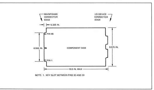
customer-designed interface boards. Slot spacing determines the type and number of customer-designed board that can be used. The six slots can accommodate six printed circuit boards or three wirewrap socket boards having the dimensional specifications shown in figure 1-3. The backplane connector edge of the boards must be designed for plugging into 130-pin (0. I-inch centers), double-row connectors.
1.11 EXPANSION CHASSIS
When more interface circuit boards are required than can be accommodated in the mainframe chassis, they can be housed in a separate expansion chassis. The backplane wiring of the expansion chassis is connected by
I/o
cable to one of the byte I/O interface connectors in the mainframe chassis through the I/O Line Driver and Receiver interface option. This circuit board option normally plugs into connector J21 in the main-frame chassis, but it can plug into any of the otherthree byte I/O connectors or two ROM connectors. The connector into which it is plugged determines the posi-tion of the expansion chassis (and all its interface units) in the hard-wired priority chain. Plugging the board into connector 121 places the expansion chassis interface units last in the priority chain.
I/O DEVICE
7
CONNECTOR EDGE
--.--COMPONENT SIDE B.575 IN.
L -________________________________ ~ _ _ ~
...
1 ... · - - - 1 0 . 5 IN. MAX - - - -... --11
[image:12.612.36.562.392.700.2]NOTE: 1. KEY SLOT BETWEEN PINS 32 AND 33
Figure 1-3. Interface Circuit Board Dimensional Data
1-6
[
[
[
[
[
[
[
, , I '[
[
[
[
[
[
[
[
[
('
[
I:
(
I
(
(
[
[
The
I/o
Line Driver and Receiver interface option shares one circuit board with the Parallel Teletype Controller interface option. The circuit board, with both options included, is shown in figure 1-4. The I/O cable connecting the expansion chassis to the main-frame chassis attaches to card edge connectors P3 and P4 (figure 1-4) on the I/O Line Driver and Receiver board. The other end of the I/O cabl~ is hard-wiredPLUGS INTO MAINFRAME BYTE I/O CONNECTOR
to a terminator board in the expansion chassis as shown in figure 1-5. The terminator board contains termination resistors for the
I/o
cable and connects the cable to the expansion chassis backplane. Two connectors on the terminator board can be used to extend the I/O bus to another expansion chassis. Detail specifications for the I/O cable are given in table 1-2.CONNECTS TO EXPANSION CHASSIS THROUGH I/O CABLE
}
PARALLEL TELETYPE CONNECTOR
P2
[image:13.612.51.580.178.479.2]NOTE: BOARD INCLUDES BOTH I/O LINE DRIVER AND RECEIVER AND PARALLEL TELETYPE OPTIONS
Figure 1-4. I/O Line Driver and Receiver Interface Option
Table 1-2. I/O Cable Specifications
Characteristic Specification
Number of conductors 88 (44 pairs)
Wire type Number 24 AWG (MIL-WI6878D) twisted pair; 1-1/2 twists per inch
Cable length 30 ft maximum
Characteristic impedance 120 ohms
Capacitance Less than 15 pF/ft
Propagation delay Approximately 1. 5 ns/ft
1-8
MAINFRAME CHASSIS
EXPANSION CHASSIS
BACKPLANE
I/O LINE DRIVER AND RECEIVER BOARD
BACKPLANE
HARD-WIRE
CONNECTION I/O CABLE
'-_...a. _ _ _ _ TO ADDITIONAL EXPANSION CHASSIS
Figure 1-5.
1/
0 Expansion Cabling[
rr
~
[
[
[
[
: . I .[
[,
[
[
[
[image:14.612.31.579.90.539.2](
[
(
[
(
(
[
(
[
I:
I
[
[
(
I
I
I
2.1 INTRODUCTION
The serial Teletype I/O interface is a standard feature of the CIP/200().series computers. A Teletype wired for four-wire, full duplex, 2().mA operation can be con-nected directly to the cable provided with the computer.
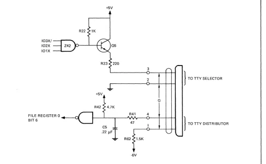
The four-wire
I/o
interface circuit is shown in figure 2-1. The transmit portion of the circuit contains a 20-mA current source that can be turned on or off depending on the state of the I/O control register. When the I/O con-trol register is in any mode other than mode 3, the out-put of gate Z42 is high, emitter follower Q5 conducts, and approximately 20 mA of current flow through resis-tor R23. This current holds the Teletype in the mark condition. When the I/O control register is set to mode 3 by a microcommand*, the output of gate Z42 is low, emitter follower Q5 cuts off, and no current flows to the Teletype.The receive portion of the interface circuit contains a low-pass filter network connecting the Teletype
*See CIP/2000 Reference Manual for a description of I/O control register operation.
Paragraphs 2. 1 to 2. 2
2. SERIAL I/O INTERFACE
distributor to bit 6 of file register 0 where it may be sensed by microcommands. One side of the Teletype distributor is -connected to -6V through resistor R62. The other side of the distributor is connected to a TTL gate, which forms bit 6 of file register O. When the Teletype sends a mark signal, the output of the gate is held low and a O-bit appears in bit 6 of file register O. When the Teletype sends a space signal, a 1-bit appears in bit 6 of file register O.
2.2 CHARACTER ASSEMBLY AND DISASSEMBLY
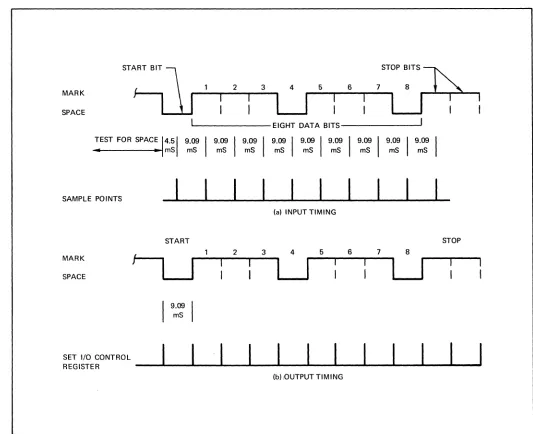
Teletype character assembly, disassembly, synchroni-zation, and timing in the CIP/2100 Computer is accom-plished by a firmware routine initiated by the macro instructions for the serial I/O interface. Figure 2-2 shows the timing for transmitting or receiving 11 ().baud Teletype characters.
During an input operation the firmware program searches for the leading edge of the start bit by continuously testing the Teletype input lines. Once a space level is detected the firmware program delays 4.5 milliseconds and then samples the input every 9.09 milliseconds until
Paragraph 2. 3
+5V
R22 1K
I 0 3 X / - - - -...
I02X 1)---'--+-1
I01X
220
3
2 } TO TTY SELECTOR
+5V
Q
R42 4.7K
R41 4 47 FILE REGISTER 0 . _ - ( ; (
BIT 6
} TO TTY DISTRIBUTOR
R62 1.5K
·6V
Figure 2-1. Serial
I/o
Interface Circuitthe eighth information bit is shifted into the assembly register. In the 2100 Computer the character is assem-bled in the least significant byte of the A-register (file register 4). The initial delay of 4.5 milliseconds after detecting the leading edge of the start bit causes sam-pling to occur in the middle of each signaling element.
During an output operation the firmware program sets the I/O control register to the appropriate mark or space condition every 9.09 milliseconds according to the start and stop bits and the data to be serially trans-mitted. Before the first information bit is transferred the
I/o
control register is set to mode 3 to transmit the start bit. The firmware program for transmitting a Teletype character remains active for 11 intervals (100 milliseconds) to assure the proper stop interval before the next character is transmitted.2.3
MICRO COMMANDS
AND MACRO INSTRUCTIONS
Two micro commands (2000 Computer) and two macro instructions (2100 Computer) affect the operation of the serial I/O interface: Load Seven Control (LS), Control (K), Input Byte Serially (IBS), and Output Byte Serially (OBS).
2-2
The Load Seven Control Microcommand gates the Teletype input to bit 6 of file register 0 during the next command time if the memory spare bit option is installed. In this case a 1701 command must be executed immediately before testing the Teletype input.
If the memory spare bit option is not installed, the serial Teletype input is constantly at bit 6 of file register O.
The Control microcommand sets the state of the I/O control register, which, in turn, establishes the mark or space of the serial Teletype output. Executing this command with bit 7 set to 1 causes the contents of bits 4 through 6 to be entered into the
I/o
control register. When the register contains a 3, the serial Teletype interface transmits a space. For all other settings of the register the serial I/O interface transmits a mark. For example, the command 7XOX causes the interfaceto go to a marking condition, while the command 7XBX causes the output to transmit a space.
The 2100 Computer Input Byte Serially macro instruction transfers an eight-bit character from the Teletype into the eight low-order bits of the A-register. The execu-tion of this instrucexecu-tion terminates when a complete
I
[
[
[
[
[image:16.612.30.555.73.396.2](
[
[
I.
[
[
I~
[
I
[
I
I
[
(
(
I
I
MARK SPACE
START BIT
J
~I
TEST FOR SPACE
14.51
9.09 • ..mS mSSAMPLE POINTS
MARK SPACE
SET I/O CONTROL
START
9.09
mS
9.09 mS
2
2 3 9.09
mS
3
Paragraph 2.4
4 5 6
U
7STOP:TS~
_"t"--....,..---.U:
EIGHT DATA BITS9.09
I
9~o;
I
9.09 9.09mS mS mS
9.09 9.09
mS mS
(a) INPUT TIMING
STOP
4 5 6 7 8
REGISTER ____ - L ____ ~ __ ~ ____ ~ __ ~L_ _ _ ~ _ _ _ _ ~ _ _ ~ _ _ _ _ ~ _ _ _ _ L _ _ _ ~ _ _ ~
(b)IOUTPUTTIMING
Figure 2-2. Serial I/O Timing
Teletype character has been received. For proper operation, the execution of the instruction must be started before the start of the Teletype character. Once the instruction is started the computer becomes tied up until a Teletype character is received. The execution time of the instruction extends approximately 84 milli-seconds after the leading edge of the Teletype character start bit. When the program echoes input characters back to the Teletype, the effective input rate cannot exceed five characters per second, since no input can be handled during the 100 milliseconds required for output.
The 2100 Computer Output Byte Serially macro instruc-tion disassembles the eight low-order bits of the A-register and transfers them serially, as a Teletype character, through the serial 1/0 interface. During the
execution of this instruction the eight low-order bits of the A-register are set to 1 's; the eight high-order bits remain unchanged.
2.4 TELETYPE INTERFACE CONNECTION
If an ASR 33 Teletype is purchased from Cincinnati, it has already been modified for use with the 2000-series computers. It can be connected to the computer simply by mating the serial I/O connector with connector S2 of the Teletype (located at the left rear).
Procedures for modifying standard ASR 33 or 35 Teletypes for use with 2000-series computers are given in appendix C.
[image:17.612.41.574.76.510.2]T
1.
1
'1
I
1
[
l'
11,
[
[
[
[
(
[
[
[
(i
[
[
[
(
(
I
[
[
3.1 INTRODUCTION
The byte I/O interfaces (both internal and external) comprise nine input data lines, five input control lines, nine output data lines, eight (internal) or ten (external) output control lines, and four spare lines. The points of interface to both the internal and external byte I/O buses and the relationships between both buses are depicted in figure 3-1. This figure shows the point of origin or destination in the processor for all interface lines. It also shows the interface logic on the
I/o
Line Driver and Receiver interface option (shown plugged into connector J21) and shows how the option is used to extend the byte I/O bus t6 an external expansion chassis.3.2
BYTE I/O BUS
The following paragraphs describe the input and output data lines and the control lines of the byte
I/o
bus. Except where specifically stated otherwise, the descrip-tions apply to both the internal and external byte 1/0 buses.Note
Throughout this manual a virgule (I)
appended to a signal or line mnemonic indicates negation; that is, the signal or line is low when the function specified by the signal or line is occurring.
3. BYTE I/O INTERFACES
3.3 INPUT DATA LINES
Input data lines
mool
throughm081
are continuous from the last interface unit on the 110 cable through the 1/0Line Driver and Receiver board, the backplane, and into the processor B-bus. A termination network for each line is located in the processor. The lines are driven by DTL power gates (944 or equivalent) with uncommitted collectors. Because of the termination network, the lines are allowed to swing only between ground and +3V. Each line is at ground potential when anyone of the DTL power gates on the line is turned on. Each line is at +3V when all gates on the line are off. When a gate is switched on, the line to which it is connected places a logical 1 onto the B-bus and into the destination register or memory.
The input data lines are handled exactly the same whether a device controller is connected to mainframe connectors J16 through J21 or to the 1/0 cable in the expansion chassis. However, when the external lines are used, they must be terminated at the remote end as well as the processor end.
3.4 OUTPUT DATA LINES
Output data lines
Tooxl
through T08X/ andODool
throughOD081
connect the processor T-register to external 1/0devices. The T-register is the physical source for output
3-2
CENTRAL PROCESSOR
B-BUS
T-REGISTER 10001
10071
TOOXf T07X!
lOIX!
PRINTED CIRCUIT BACKPLANE
JI6THRUJ20
110 LINE DRIVE AND RECEIVER INTERFACE
OPTlONJ21
EXPANSION CHASSIS OR
CUSTOMER EQUIPMENT
CO~~~Oll-""0",2X,-1 - - - - , - - - - ' - - - - ' - - - - , - - t
REGISTER
Mise CONTROL
lQ3X!
CPHI
CPH2!
CSTP/ MRESI FilE REGISTER 0
BIT3 EClot
T-REGISTER
(BIT81
10081
~~.E~~R~/--~~jJ_-_-_-_jJL-r-
______________
-T:+P __
4P~:
__
~
__
-L~:
EJ
II
II
I:
+
I
p pI ""
I
PRllIl PRI1I PRI1{ PRill:
I I:
I./.-r---'-=t-O/ / /<>---t---="-+-_ +_ - - - l - , t - - - t - - j
IPROIl PRO 11 PR011
J:
p P OJ,. I :_ _ _ _ _ _ _ _ _ _ : _ _ _ _
---=P.=---I1~+---1:
1r--1t-+:
-J,----+:
-~
C
I=
II
I
Figure 3-1. Byte
I/o
Interface, Simplified Logic DiagramTERMINATION NETWORK
- -
-(1'",
...
[
[
[
[
[
[
[
[
[
[
[
I
[
[
[
[
[
[image:20.612.33.564.65.704.2](:
[
[
[
[
(
[
[
[
I
I:
I:
r
[
[
(
[
data. Data or address information to be transferred to an I/O device is first fetched from the A-register, the B-register, or memory and then placed in the T -register. From the T-register it is transferred to the I/o device.
Lines TOOX/ through T07X/ are available at mainframe byte I/o connectors Jl6 through J21. (Line TOSX/ is available at the same connectors only if the spare bit option is installed in the processor.) Lines ODOO / through ODOS/ are the external byte I/o equivalent of lines TOOX/ through T08X/. They carry the same signals (slightly delayed) through the I/O cable to the expansion chassis.
To preserve the expansion capability of the output data bus, each device controller on the bus is restricted to a single unit load (one DTL or TTL gate) or 1. 6 rnA maxi-mum on each output data line. Both the TOXX/ and ODXX/ lines have the following characteristics:
T -Register Content TOXX/ ODXX/
Binary 1 OV OV
Binary 0 +4V (nom) +3V (nom)
3.5 INPUT CONTROL LINES
The five input control lines available at the byte I/O interface are:
a. ECIO/ - concurrent I/o request
b. ERPY / - I/O reply
c. EINT / - external interrupt
d. EDPR/ - external device protect
e. PRIll - priority return
All five lines are continuous from the last interface unit on the I/o cable, through the I/O Line Driver and Receiver board, the backplane, and into the processor. The lines are driven by DTL power gates (944 or equiv-alent) with uncommitted collectors. A termination net-work for each line is included in the processor. Because of the termination networks, the lines are allowed to swing only between ground and +3V. All five lines are active, or indicate assertion, when they are at ground potential. For example, ground potential on line EINT/ causes an external interrupt.
Input control lines ECIO/, ERPY/, and EINT/ provide inputs to file register 0 in the processor. The status of these lines can be determined in the microprogram by testing the associated bits of the file register.
Line ECIO/ becomes bit 3 of file register 0, where it acts as an interrupt to the CIP/2100 processor. It causes
Paragraphs 3.5 to 3.6
the processor to discontinue normal instruction execution and begin a firmware subroutine for handling a concur-rent data transfer.
Line ERPY / becomes bit 5 of file register O. This bit is not currently used in the CIP /2100 processor. It is included for those system designers who may want to effect their own microprogrammed I/O transfers (since file register 0 bits are testable only at the micro-program level).
Line EINT/ is the external interrupt line, which is shared by all Priority Interrupt boards and device con-trollers. It becomes bit 7 of file register O. It causes
the CIP/2100 processor to discontinue normal instruc-tion execuinstruc-tion and begin a firmware sequence to deter-mine the address of the interrupting device. (See paragraph 3.28 for a description of external interrupt operation.)
Line EDPR/ is activated by an I/o device during input transfers to override the optional memory protection error interrupt. It Signifies that the device has been programmed to transfer data into a protected area of memory.
Line PRIll is the priority input line from the next higher priority controller. It is used by each controller in determining priority before requesting an external inter-rupt or concurrent I/O request. (See paragraph 3.29 for a description of priority determination. )
3.6 OUTPUT CONTROL LINES
Of all the interface lines only the output control lines are functionally different at the internal and external byte I/o interfaces. The following lines are available at each interface:
Internal Interface External Interface
IOlX/ COXX/
I02X/ DOXX/
103X/ SPl/
CPHl SP2/
~PH2/ 10AK/
MRES/ DIXX/
PROl/ SP3/
KOXX/
MRES/
PROl/
Paragraph 3. 7
3.7 Internal Byte I/O Control Lines (Mainframe Chassis)
Internal
I/o
control lines IOIX/ through I03X/ originate at the false outputs of the three I/O control flip-flops in the processor. These flip-flops are set and reset at the microcommand level. The eight states that the flip-flops can assume are assigned meanings to indicate v!iriousI/o
control modes. Definitions of the eight controlflip-flop states for the CIP /2100 are given in table 3-1. Other definitions can be applied for specialized CIP /2000 configurations.
As shown in figure 3-1, lines IOIX/ through I03X/ are decoded on the I/O Line Driver and Receiver board, and seven lines are then available (state 0 is not used) at the external interface. A device controller designed for use in the mainframe chassis must decode these three lines as is done on the
I/o
Line Driver and Receiver board.Device controllers designed for the CIP /2100 processor are required to decode only states 1 (COXXI), 2 (DOXXI), 5 (IOAKf), and 6 (DIXXf). These states represent
Table 3-1. I/O Control States
State Control Definition Logic Term
0 None None
1 Control output COXX/
2 Data output DOXX/
3 Space serial Teletype SPI/
4 Spare SP2/
5 I/O acknowledge IOAK/
6 Data input DIXX/
7 Spare SP3/
220 nS ---CPH1
~~
________~
.--CPH2/
I
control output, data output, I/O acknowledge, and data input functions, respectively.
It is important to remember that a device controller in the mainframe chassis must decode the I/O control flip-flop lines, but one in the expansion chassis does not, since the external bus is used to connect the two chassis.
Lines CPRI and CPR2/ provide processor clock signals to device controllers connected to the mainframe byte I/O connectors. Each line can be used independently as a square wave source (4.55 MHz), or they may be used together in a NAND gate to produce a 35-ns clock pulse (CPRI is inverted and delayed 35 ns from CPR2/). The relationship of the signals on lines CPRl and CPR2/ is shown in figure 3-2.
Control line CSTP / of the internal byte
I/o
interface carries a signal to indicate that the internal processor clock has been stopped for either of the following reasons:a. The processor is halted.
b. The processor is executing a logical pause (for 1 to 5 clock times) while performing a jump or attempting to overrun a memory operation during a microcommand sequence.
Line CSTP / is available to gate clocks in device control-lers when intimate micro level control of a device is' required. It is not included in standard byte
I/o
inter-faces and must be jumpered to an open pin of an option board connector if its use is required.Control line MRES/ is the master reset line. It is activated by the RESET switch on the operator's console, or by the optional power fail circuit during power failure or restart. It is used to clear all control flip-flops to their initialized conditions. Ground potential is applied to this line when the RESET switch is pressed.
-I
I
J
L
-
L35"'
U
U
I-
220 nS..
\Figure 3-2. Relationship of Control Signals CPRl and CPR2/
3-4
[
[
[
[
[
, ..
I •
II
..
[
~'
[image:22.612.25.561.317.696.2](
[
[
[
[
I'
I:
I:
I
I:
('
(
[
I
[
I
Control line PROI/ carries the priority signal from controller to controller. It becomes line PRIll at the input of the next lower priority controller. Backplane strapping on the mainframe chassis determines the rela-tive priority of devices on the I/O bus. A modification of the strapping permits interface units in the mainframe chassis to have lower priority (for interrupt or concur-rent I/O operations) than units in the expansion chassis at the end of the I/O cable. (See paragraph 3.29 for a description of priority determination. )
3.8 External Byte I/O Control lines (I/O Cable)
Figure 3-1 shows how the output control lines are modi-fied in the I/O Line Driver and Receiver board to develop the control lines available in the I/O cable. As explained in the preceding paragraph, lines I01X/ through I03X/ are converted into unitary control lines. The main reason for this conversion is the elimination of ambi-guity resulting from flip-flop crossover variations. These crossover variations could produce spikes that would cause incorrect operation if the decoded terms were used as clocks. This problem can be overcome in the mainframe chassis by using a synchronous clock created from signals CPHI and CPH2/. Since this solu-tion is unacceptable at the end of the I/o cable, the out-puts of the three I/O control flip-flops are converted into seven unitary lines on the I/o Line Driver and Receiver board after crossover skew has been eliminated.
Of the seven decoded control lines available at the I/O cable, only four are presently used for byte I/O opera-tions: COXX/, DOXX/, IOAK/, and DIXX/. Lines SPI/, SP2/, and SP3/ are spare control lines that are not used in the CIP /2100. They can be used to carry I/O control signals originated by special firmware.
Note
Although control line SP1/ is considered a spare, it represents I/O control state 3, which is the space serial Tele-type mode. This line can be used only in the absence of the serial Teletype.
Control line COXX/ carries a low signal to specify that a control byte containing a device number and device order is on the output data lines. The device being addressed accepts the byte and decodes the order.
Control line DOXX/ carries a low signal to specify that an information byte is on the output data lines. The pre-viously addressed device accepts the byte.
Control line IOAK/ carries a low signal to acknowledge a request from an I/O device for an interrupt (para-graph 3. 28) or a concurrent I/O transfer (para(para-graph 3.25) . The requesting device uses the Signal to transfer
an
address byte on the input data lines to the processor.
Paragraphs 3. 8 to 3. 12
Control line DrxX/ carries a low signal that is used by a previously addressed I/O device to transfer an infor-mation byte on the input data lines to the processor.
Control line KOXX/ carries a 2. 275-MHz, 50% duty cycle clock signal that can be used by external devices for timing.
Control lines MRES/ and PROI/ have the same meaning in the I/O cable as they do for the internal byte I/O interface.
3.9 SPARE LINES
Spare lines SP4 through SP7 are continuous from the last interface unit on the I/O cable, through the I/o Line Driver and Receiver board, and onto the backplane. These lines are not terminated in any way and are pro-vided only for special customer requirements.
3.10
BYTE
I/O
FUNDAMENTALS
Although the flexibility of the byte I/O system lends itself to customizing for individual applications, certain standard conventions have been adopted for byte I/O operations in the CIP/2100 Computer. These conven-tions are described in the following paragraphs.
3.11 DEVICE ADDRESSING
Each I/O device on the byte I/O bus is assigned a unique five-bit device address or number. On most CIP device controllers, the addresses are selected by the placement of jumper wires on the printed circuit board of the controller.
Each device controller on the I/o bus determines if it is being addressed by comparing its assigned address to the five-bit device number in the control byte sent to all controllers on the output data lines. The device number portion of the control byte appears on data lines TOOX/ through T04X/ (ODOO/ through OD04/). The assigned device address is also used to identify the I/O device requesting an interrupt or concurrent I/O transfer. The processor acknowledges each request with signal 10AK/. On receiving the acknowledgement signal, the requesting device places its address (times 2) on input data lines IDOl! through ID05/.
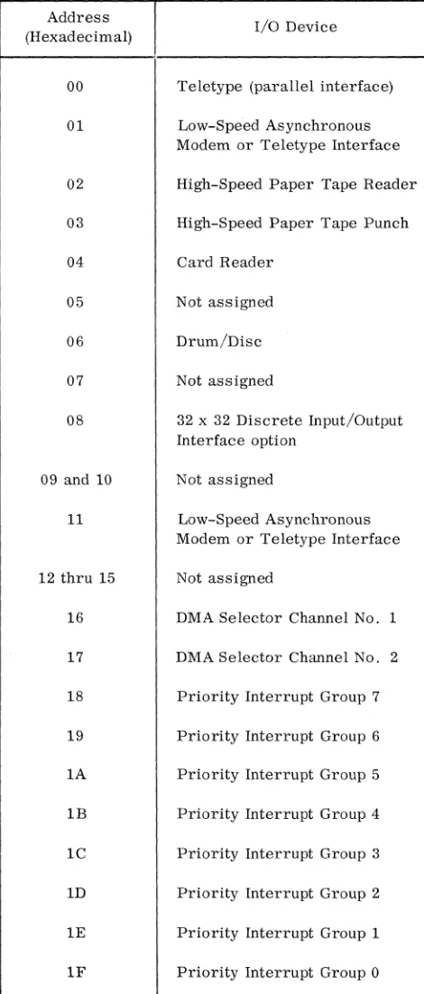
Table 3-2 lists the device addresses assigned to CIP/2100 standard interface units. Customer-designed controllers should not use the assigned addresses if the use of standard CIP controllers is planned.
3.12 DEVICE ORDERS
Accompanying the five-bit device address in the control byte sent to all devices before each programmed transfer is a three-bit device order specifying the I/o operation
Paragraphs 3. 13 to 3. 17
Table 3-2. Standard
I/o
Device AddressesAddress
I/o
Device (Hexadecimal)00 Teletype (parallel interface)
01 Low-Speed Asynchronous Modem or Teletype Interface
02 High-Speed Paper Tape Reader
03 High-Speed Paper Tape Punch
04 Card Reader
05 Not assigned
06 Drum/Disc
07 Not assigned
08 32 x 32 Discrete Input/Output Interface option
09 and 10 Not assigned
11 Low-Speed Asynchronous Modem or Teletype Interface
12 thru 15 Not assigned
16 DMA Selector Channel No. 1
17 DMA Selector Channel No. 2
18 Priority Interrupt Group 7
19 Priority Interrupt Group 6
lA Priority Interrupt Group 5
IB Priority Interrupt Group 4
lC Priority Interrupt Group 3
1D Priority Interrupt Group 2 IE Priority Interrupt Group 1
IF Priority Interrupt Group 0
to be performed by the device. The device order portion of the control byte appears on output data lines T05X/ through T07X/ (OD05/ through OD07/). A list of stand-ard device orders is given in table 3-3. Not all device controllers are required to use all the orders listed in the table. Their use is dictated by controller design.
3-6
3.13 STATUS BYTES
In response to a status order from the processor, the addressed I/O device places a status byte on input data lines moo/ through m07/.. Four of the status bits are common to all device controllers; the other four are device dependent and differ from controller to controller. The status byte is transferred into the A-register, the B-register, or memory by an input instruction with device order l. The significance of each bit in the status byte is described in table 3-4.
3.14
BYTE
I/O
OPERATIONS AND TIMING
The following paragraphs describe the
program-controlled and concurrent I/O operations ofthe CIP/2100 Computer. Timing diagrams are included for each operation, and typical controller logic for performing the operations is also shown. For a description of the I/O instructions that pertain to the byte I/O operations, consult the CIP/2100 Reference Manual.
3.15 PROGRAM-CONTROLLED I/O OPERATIONS 3.16 Data Output Timing
The timing diagram for a typical data output operation is shown in figure 3-3. When an output byte instruction (OBA, OBB, or OBM) is executed, the second byte of the instruction containing the device address and order is placed on output data lines TOOX/ through T07X/ (ODOO/ through OD07/). Approximately 220 ns later, control line COXX/ goes low to indicate the presence of a control byte on the output data lines. During the 880 ns that line COXX/ is low, each device controller on the bus examines lines TOOX/ through T04X/ (ODOO/ through OD04/) to determine if it is the controller being addressed. The controller whose address is on the lines connects itself for service and decodes and stores the device order on output data lines T05X/ through T07X/ (OD05/ through OD07/). When the controller is connected for service, it is susceptible to either data output or data input sig-nals from the processor and transfers data accordingly. Once connected for service, the controller remains con-nected until a data output or data input signal occurs.
After removing the control output signal and control byte from the lines, the processor places a data byte on the output data lines. Approximately 220 ns later, data out-put line DOXX/ goes low to indicate the presence of data on the lines. The controller then strobes the data byte from the output data lines into its data register. When line DOXX/ again goes high, the controller disconnects itself from further service.
3.17 Typical Data Output Logic
The timing diagram of figure 3- 3 can be related to the typical data output logic shown in figure 3-4. The eight
[
[
[
I
[
[
[I
I 1
[
[I
[
[
[
[
[
[
[
[
I;
[
I
[
[
I
I
[
Order Number
o
1
2 3
4 5 6 7
Bit Number
o
1
2
3 4-7
Operation
Data
Status /function
Block input
Block input with interrupt
Stop
Protect state
Block output
Block output with interrupt
Condition
Ready
Input flag
Output flag
Error
Undefined
Table 3-3. Standard I/O Device Orders
Description
The data order causes a data byte to be transferred between the processor and the addressed device. The direction of transfer depends on the type of instruction (input or output).
The status/function order causes a status byte to be transferred from the addressed device to the processor, or a function byte to be trans-ferred from the processor to the device depending on the type of instruction (input or output).
The block input order notifies the device to proceed with a concurrent block input to memory. This order can be sent with either an input or an output instruction.
The block input with interrupt order notifies the device to proceed with a concurrent block input to memory and to generate an interrupt at the end of the transfer. This order can be sent with either an input or output instruction.
The stop order causes the block input or output operation in progress to be stopped. An external interrupt is generated'if an interrupt would normally have been generated at the end of the block transfer.
The protect state order allows the device to write into protected areas of memory with concurrent input. The device is taken out of this mode at the end of the transfer.
The block output order notifies the device to proceed with a concurrent block output from memory. This order can be sent with either an input or an output instruction.
The block output with interrupt order notifies the device to proceed with a concurrent block output from memory and to generate an interrupt at the end of the transfer. This order can be sent with either an input or an output instruction.
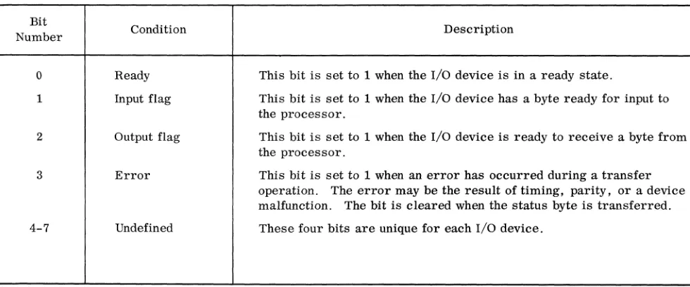
Table 3-4. I/O Device Status Byte Definition
Description
This bit is set to 1 when the I/O device is in a ready state.
This bit is set to 1 when the I/O device has a byte ready for input to the processor.
This bit is set to 1 when the I/O device is ready to receive a byte from the processor.
This bit is set to 1 when an error has occurred during a transfer operation. The error may be the result of timing, parity, or a device malfunction. The bit is cleared when the status byte is transferred.
These four bits are unique for each
I/o
device. [image:25.612.74.564.522.726.2]3-8
FUNCTION CODE AND
1
\ LDATATRANSFER
DEVICE ADDRESS OCCURS HERE
TRANSFER OCCURS HERE
OUTPUT DATA LINES
I
I
f---1
TOOX/-T08X/ '
1
..
_ & - . _ _ - - '(ODOO/-OD08/)
11.32
I-IS-4-:---'-0I--1.32 I-Is---I 880 nS MIN4.4p.S MAX 220 nS ~
CONTROL OUTPUT COXX/
DATA OUTPUT DOXX/
~p----~Jl~---I--
--I
I--
220 nS---~Jl~---~p---880 nS--/
880 nS--I
~
Figure 3-3. Data or Function Output Timing
DEVICE ADDRESS DECODING
I/O BUS OUTPUT DATA LINES
I/O BUS CONTROL { lINES*
ODOO/ I
I
I OD04/
OD05/ }
FIGURE 3-5 OD07/
DAOO
CONTROL RECEIVERS CONNECT FOR SERVICE
n-D_S_T_R_/ __ DATA STROBE TO REGISTER * THESE LINES AVAILABLE AT OUTPUT OF I/O LINE DRIVER BOARD ONLY.
IF THIS BOARD IS NOT USED. THESE LINES MUST BE CREATED BY DECODING I/O CONTROL LINES 101X/. 102X/. AND 103X/.
Figure 3-4. Data Output Logic
CONN
[
[
[
[
[
1
[
[image:26.612.36.557.71.690.2]I
[
I
[
[
I'
[
I
I
I
I
I
I
[
I
[
output data lines are connected to eight TTL or DTL inverters in the device controller. Each output line is buffered by an inverter or gate to minimize the loading on the line and to allow for expansion to the full number of devices. Receiver outputs ODOO
I
throughOD041
are applied to an address decoding circuit. In the example shown, the circuit is connected to decode a device address of 00 (all false terms are used).Control lines
coxxl
andDoxxl
are used for dual purposes in the example logic. Signal COXX is used as a qualifying signal in the addressing decoding circuit, and its complementcoxxl
is used to clock the connect-for-service flip-flop. SignalDoxxl
is also used to clock the connect-for-service flip-flop and its complement (DOXX) generates the signal for strobing data into the controller register.When the connect-fo. '-service flip-flop sets, the con-troller is receptive to the actual transfer of data (the second phase of the data output operation). The signal for gating the output data lines into a device register or similar storage device is generated by the connect-for-service signal and control signal DOXX (data output). As figure 3-3 indicates, signal
Doxxl
occurs anywhere from 880 ns to 4.4 /-Is maximum after the device address is removed from the output data lines. The timing varies because the output data can originate in the A-register, the B-register, or memory.3.18 Function Output Timing
The timing diagram shown in figure 3-3 for a data output operation is also valid for a function output operation. The function output operation is typically used to control a discrete action in an
I/o
device for which data transfer is not required. Rewinding tape is an example of such an action. The most efficient way to perform this opera-tion is to issue a single instrucopera-tion containing all the information necessary to alert the device and cause the tape to rewind.In the CIP/2100 Computer the output byte instructions (OBA, OBB, and OBM) are also used to perform the function output operation. The only difference in the instructions is the assignment of the f-code (bits 5 through 7) in the control byte of the instruction.
When an output byte instruction is used for function out-put, the f-code of the control byte deSignates the unique function in the 1/0 device to be controlled. The assign-ment of f-codes for function operations precludes the use of the same codes for data transfer operations.
The function output operation is executed exactly like the data output operation described in paragraph 3.16. In fact, a data byte is transferred from either the A-register, B-register, or memory depending on the output byte instruction used. This data byte is usually ignored by the device controller, since the f-code of the control byte contains enough information to describe most function operations. However, should a controller require more
Paragraphs 3. 18 to 3. 20
function definition than is possible in the control byte, the data byte transferred during the function operation could be used to carry additional function information.
3.19 Tvpical Function Output Logic
The alerting of the device controller by sending the control output signal
(COXX/)
along with the device address is accomplished exactly as described for data output. When linecoxxl
goes low, the controller examines bits 5 through 7(OD051
through OD07I)
of the control byte and, if necessary, stores them so that it can perform the ordered function. Figure 3-5 shows typical logic for storing and then decoding the function bits. An alternative method would be to decode the func-tion bits first (during DAOO time) and then store the decoded results in unitary flip-flops. This method would be advantageous when several control states are required, each one executing a separate function and each one having an asynchronous reset term dependent on the device.The important point to remember is that functions needed for longer than 880 ns must be stored either before or after decoding. A suitable clock for storing this infor-mation is signal DAOO, derived from the device address bits and signal COXX.
3.20 Data Input Timing
The timing diagram for a typical data input operation is shown in figure 3-6. When an input byte instruction (IBA, IBB, or IBM) is executed, a two-phase data input operation, similar to data output, is performed. The first phase is identical to the first phase of the data out-put operation. The control byte containing the device address and order is placed on output data lines
Tooxl
throughT07Xl (ODOOI
through OD07I)
by the processor, and then control output linecoxxl
goes low. At that time the device controller connects itself for service and prepares to transfer data to the processor on input data linesmool
throughm08/.
In terms of controller deSign, the device controller is not required to detect, during the device address phase, whether an input or output operation is to be performed. It can connect itself for service in either case and then allow the data input(DIXX/)
or data output(DOXX/)
control lines to direct its further activity.As shown in figure 3-6, approximately 880 ns after the control byte is removed from the output data lines, data input line
DIXXI
goes low for 880 ns. Device data to be transferred to the processor must be settled no later than 440 ns after lineDIXXI
goes low. The data byte can be applied to the input data lines as early as the beginning of signalcoxx/.
For interface design free-dom, the input data may be applied even during an output byte instruction with no adverse effect.The input data must be removed from the input data lines no later than 440 ns after line