Faculty of Electrical and Computer Engineering
Chair of Highly-Parallel VLSI Systems and Neuro-Microelectronics
Diploma Thesis
DYNAMIC INSTRUCTION SET
EXTENSION OF MICROPROCESSORS
WITH EMBEDDED FPGAS
Heiner Bauer
Born on: November 20, 1991
to achieve the academic degree
Diplomingenieur (Dipl.-Ing.)
Supervisors
Dr.-Ing. Sebastian Höppner
Dr.-Ing. Johannes Partzsch
Supervising professor
Prof. Dr.-Ing. habil. Christian Mayr
STATEMENT OF AUTHORSHIP
I hereby certify that I have authored this diploma thesis entitled Dynamic instruction set extension of microprocessors with embedded FPGAsindependently and without undue as-sistance from third parties. No other than the resources and references indicated in this diploma thesis have been used. I have marked both literal and accordingly adopted quota-tions as such. During the preparation of this thesis I was supported by:
Dr.-Ing. Sebastian Höppner as a supervisor Dr.-Ing. Johannes Partzsch as a supervisor
Florian Schraut of Racyics GmbH with all layout tasks Additional persons were not involved in the preparation of the present thesis. Dresden, March 23, 2017
ABSTRACT
Increasingly complex applications and recent shifts in technology scaling have created a large demand for microprocessors which can perform tasks more quickly and more energy efficient. Conventional microarchitectures exploit multiple levels of parallelism to increase instruction throughput and use application specific instruction sets or hardware accelerators to increase energy efficiency. Reconfigurable microprocessors adopt the same principle of providing application specific hardware, however, with the significant advantage of post-fab-rication flexibility. Not only does this offer similar gains in performance but also the flexibility to configure each device individually.
This thesis explored the benefit of a tight coupled and fine-grained reconfigurable micro-processor. In contrast to previous research, a detailed design space exploration of logical architectures for island-style field programmable gate arrays (FPGAs) has been performed in the context of a commercial 22 nm process technology. Other research projects either reused general purpose architectures or spent little effort to design and characterize custom fabrics, which are critical to system performance and the practicality of frequently proposed high-level software techniques. Here, detailed circuit implementations and a custom area model were used to estimate the performance of over 200 different logical FPGA architec-tures with single-driver routing. Results of this exploration revealed similar tradeoffs and trends described by previous studies. The number of lookup table (LUT) inputs and the structure of the global routing network were shown to have a major impact on the area delay product. However, results suggested a much larger region of efficient architectures than before. Finally, an architecture with 5-LUTs and 8 logic elements per cluster was se-lected. Modifications to the microprocessor, which was based on an industry proven instruc-tion set architecture, and its software toolchain provided access to this embedded reconfig-urable fabric via custom instructions. The baseline microprocessor was characterized with estimates from signoff data for a 28 nm hardware implementation. A modified academic FPGA tool flow was used to transform Verilog implementations of custom instructions into a post-routing netlist with timing annotations. Simulation-based verification of the system was performed with a cycle-accurate processor model and diverse application benchmarks, ranging from signal processing, over encryption to computation of elementary functions.
For these benchmarks, a significant increase in performance with speedups from 3 to 15 relative to the baseline microprocessor was achieved with the extended instruction set. Except for one case, application speedup clearly outweighed the area overhead for the ex-tended system, even though the modeled fabric architecture was primitive and contained no explicit arithmetic enhancements. Insights into fundamental tradeoffs of island-style FPGA architectures, the developed exploration flow, and a concrete cost model are relevant for the development of more advanced architectures. Hence, this work is a successful proof of concept and has laid the basis for further investigations into architectural extensions and physical implementations. Potential for further optimization was identified on multiple levels and numerous directions for future research were described.
KURZFASSUNG
Zunehmend komplexere Anwendungen und Besonderheiten moderner Halbleitertechnolo-gien haben zu einer großen Nachfrage an leistungsfähigen und gleichzeitig sehr energieef-fizienten Mikroprozessoren geführt. Konventionelle Architekturen versuchen den Befehls-durchsatz durch Parallelisierung zu steigern und stellen anwendungsspezifische Befehlssät-ze oder Hardwarebeschleuniger zur Steigerung der Energieeffizienz bereit. Rekonfigurier-bare Prozessoren ermöglichen ähnliche Performancesteigerungen und besitzen gleichzeitig den enormen Vorteil, dass die Spezialisierung auf eine bestimmte Anwendung nach der Herstellung erfolgen kann.
In dieser Diplomarbeit wurde ein rekonfigurierbarer Mikroprozessor mit einem eng gekop-pelten FPGA untersucht. Im Gegensatz zu früheren Forschungsansätzen wurde eine um-fangreiche Entwurfsraumexploration der FPGA-Architektur im Zusammenhang mit einem kommerziellen 22 nm Herstellungsprozess durchgeführt. Bisher verwendeten die meisten Forschungsprojekte entweder kommerzielle Architekturen, die nicht unbedingt auf diesen Anwendungsfall zugeschnitten sind, oder die vorgeschlagenen FGPA-Komponenten wur-den nur unzureichend untersucht und charakterisiert. Jedoch ist gerade dieser Baustein ausschlaggebend für die Leistungsfähigkeit des gesamten Systems. Deshalb wurden im Rahmen dieser Arbeit über 200 verschiedene logische FPGA-Architekturen untersucht. Zur Modellierung wurden konkrete Schaltungstopologien und ein auf den Herstellungsprozess zugeschnittenes Modell zur Abschätzung der Layoutfläche verwendet. Generell wurden die gleichen Trends wie bei vorhergehenden und ähnlich umfangreichen Untersuchungen beob-achtet. Auch hier wurden die Ergebnisse maßgeblich von der Größe der LUTs (engl. "Look-up Tables") und der Struktur des Routingnetzwerks bestimmt. Gleichzeitig wurde ein viel breiterer Bereich von Architekturen mit nahezu gleicher Effizienz identifiziert. Zur weiteren Evaluation wurde eine FPGA-Architektur mit 5-LUTs und 8 Logikelementen ausgewählt. Die Performance des ausgewählten Mikroprozessors, der auf einer erprobten Befehlssatzarchi-tektur aufbaut, wurde mit Ergebnissen eines 28 nm Testchips abgeschätzt. Eine modifizierte Sammlung von akademischen Softwarewerkzeugen wurde verwendet, um Spezialbefehle auf die modellierte FPGA-Architektur abzubilden und eine Netzliste für die anschließende Simulation und Verifikation zu erzeugen.
Für eine Reihe unterschiedlicher Anwendungs-Benchmarks wurde eine relative Leistungs-steigerung zwischen 3 und 15 gegenüber dem ursprünglichen Prozessor ermittelt. Obwohl die vorgeschlagene FPGA-Architektur vergleichsweise primitiv ist und keinerlei arithmeti-sche Erweiterungen besitzt, musste dabei, bis auf eine Ausnahme, kein überproportionaler Anstieg der Chipfläche in Kauf genommen werden. Die gewonnen Erkenntnisse zu den Abhängigkeiten zwischen den Architekturparametern, der entwickelte Ablauf für die Ex-ploration und das konkrete Kostenmodell sind essenziell für weitere Verbesserungen der FPGA-Architektur. Die vorliegende Arbeit hat somit erfolgreich den Vorteil der untersuchten Systemarchitektur gezeigt und den Weg für mögliche Erweiterungen und Hardwareimple-mentierungen geebnet. Zusätzlich wurden eine Reihe von Optimierungen der Architektur und weitere potenziellen Forschungsansätzen aufgezeigt.
CONTENTS
1 Introduction 1 1.1 Purpose . . . 2 1.2 Scope . . . 3 2 Background 4 2.1 Reconfigurable Computing . . . 4 2.1.1 Classification . . . 4 2.1.2 Academic Systems . . . 6 2.1.3 Commercial Systems . . . 8 2.2 FPGA Architecture . . . 92.2.1 Global Routing Network . . . 10
2.2.2 Local Routing and Logic Element . . . 12
3 FPGA Architecture Exploration 14 3.1 Preliminaries . . . 14
3.1.1 CAD tools . . . 15
3.1.2 Transistor Level Implementation . . . 18
3.1.3 Area model . . . 25
3.2 Exploration Setup and Results . . . 27
3.2.1 Benchmarks and CAD settings . . . 27
3.2.2 Evaluation Methodology and Parameter Selection . . . 29
3.2.3 Results . . . 31
3.2.4 Discussion and Candidate Architecture . . . 37
4 Microprocessor Integration 40 4.1 Microprocessor architecture . . . 40
4.2 Hardware Integration . . . 41
4.2.1 Reconfigurable Functional Unit . . . 42
4.2.2 Instruction Control . . . 43
4.3 Software Integration . . . 44
4.3.1 Instruction Format . . . 45
4.3.2 High-Level Interface . . . 45
4.4 Array Size Tradeoffs . . . 46
5 Application Benchmarks and Results 49 5.1 Benchmark Selection and Evaluation Methodology . . . 49
5.1.1 Fast Fourier Transformation . . . 50
5.1.2 Data Encryption Standard . . . 52
5.1.3 Exponential function . . . 53
5.2 Functional verification . . . 55
5.3 Results . . . 56
6 Discussion and Outlook 59 6.1 Discussion of Results . . . 59
6.2 Extensions and Future Research . . . 60
Bibliography 62
SYMBOLS AND NOTATION
Fc,in Fraction of routing tracks per cluster input
Fc,local Flexibility of cluster crossbar
Fc,out Fraction of available routing tracks per cluster output
FS Flexibility of switch block
I Number of cluster inputs
K Number of inputs per LUT
L Length of a routing segment
N Number of logic elements per cluster
W Number of routing tracks per channel
g Logical effort of a stage
h Electrical effort of a stage
p Parasitic delay of a stage
fopt Stage effort that minimizes delay
D Normalized path delay
S Number of stages along the considered path
ACRONYMS
ALU Arithmetic Logical Unit
ASIC Application Specific Integrated Circuit
ASIP Application Specific Instruction set Processor
BLIF Berkeley Logic Interchange Format
CAD Computer Aided Design
CB Connection Block
CGRA Coarse-Grained Reconfigurable Array
CMOS Complementary Metal Oxide Semiconductor
COFFE Circuit Optimization For FPGA Exploration
DES Data Encryption Standard
DFT Discrete Fourier Transformation
eFPGA embedded FPGA
FDSOI Fully Depleted Silicon-On-Insulator
FFT Fast Fourier Transformation
FIR Finite Impulse Response
FPGA Field Programmable Gate Array
ISA Instruction Set Architecture
LE Logic Element
LSU Load Store Unit
LUT Lookup Table
MOPS Million Operations Per Second
MWTA Minimum-Width Transistor Area
PLB Processor Local Bus
RFU Reconfigurable Functional Unit
RTL Register Transfer Level
SB Switch Block
SOC System On Chip
SRAM Static Random Access Memory
VPR Versatile Place and Route
1 INTRODUCTION
Since the dawn of digital integrated circuits, microprocessors have been a popular choice to solve complex tasks. Covering a large spectrum, from minimal 8-bit embedded processors in household appliances to 64-bit multi-core machines in supercomputers, their ubiquitous presence today shows the success of this design style. Advances in transistor process tech-nology and coordinate refinements in microprocessor architecture have allowed software systems to become increasingly complex. Groundbreaking innovations like the Internet, smartphones or modern advanced driver assistance systems all rely on powerful hardware to effectively handle the numerous levels of abstraction. Nevertheless, the end of Den-nard scaling has lead to a radical shift in the design of processor architectures [EBA+11]. Limited scaling of the power density per transistor necessitates parallel processing archi-tectures, highly energy-efficient computations, and sophisticated voltage and frequency scaling schemes [HSE+12]. Furthermore, a number of innovative and diverse approaches are being pursued to extract performance primarily from scaling in terms of silicon area.
Even without these recent complications, designing and implementing general purpose microprocessors and choosing the right combination of instructions has always been a chal-lenge [Col06]. To justify the high cost and long turnaround time, not only of logical design but also of verification, physical design, and fabrication, the final product has to perform well on a wide range of possible applications to be economically viable. Still, the limited set of available instructions provides only inefficient implementations for a number of attractive applications. Modern systems thus try to enhance performance by increasing instruction throughput and by exploiting threlevel parallelism with multi-core systems. These ad-vanced architectures are not only challenging to design and to debug, but they also scale poorly for applications with limited parallelism.
A different approach is to incorporate special purpose hardware accelerators for tasks that occur frequently, e.g., graphics rendering [HMB+14], packet processing [Cav16], or
database analytics [KLS+16]. Modern technology scaling has allowed even embedded mi-croprocessors, which are traditionally designed to be highly cost effective, to include appli-cation specific accelerators for encryption and signal processing [Tex16] or error correction, true random number generation, and cryptographic hashing [STM16].
Likewise, application specific instruction set processors (ASIPs) augment a baseline mi-croprocessor with custom instructions which are tailored to one specific application. Choos-ing the right set of custom instruction is usually carried out with the help of a cycle-accurate simulation model and a set of representative benchmark applications. Careful selection and appropriate implementation of these custom instruction can leverage details of the target application in early design stages and dramatically increase the computational performance and energy efficiency [HAN+16]. However, this approach also faces the same tradeoffs be-tween flexibility and performance and is much more sensitive to requirement changes in the target application.
Technology scaling has also enabled a quite different design style, namely reconfigurable digital circuits. FPGAs, the most prominent representative of this group, allow the end user to implement custom digital circuits without the need for expensive and time consuming design of application specific integrated circuits (ASICs). Nevertheless, the high flexibility of such fine-grained fabrics, which allow individual applications to be optimized at bit level,
1.1 Purpose
incurs significant drawbacks regarding silicon area, power consumption and maximum op-erating frequency compared to equivalent ASIC solutions [KR09].
Consequently, combining reconfigurable circuits with software programmable micropro-cessors offers a compelling solution, with sufficient flexibility to target a wide range of ap-plications. Applications can be partitioned to offload control flow operations, which are hard to design at bit level, onto the microprocessor and use the reconfigurable fabric to imple-ment datapath operations. Ideally, this would combine the advantages of general purpose microprocessors and ASIPs, but also add the exceptional capability to program individual devices with application specific instructions after fabrication. Within minutes, a designer could explore multiple custom instructions during the development phase or improve exist-ing implementations after they have been shipped and integrated into a system.
1.1 PURPOSE
Multiple implementation styles for such reconfigurable computing platforms exist and a number of different architectures and tools have been studied. Despite a multitude of projects and many attempts, not a single concept has had a long-lasting success, neither in a commercial nor in an academic context. Important problems which need to be addressed include: design and optimization of the reconfigurable fabric, development of suitable com-puter aided design (CAD) software to produce high quality results, and system integration of the fabric with existing hardware and software toolchains. Most previous research regarding reconfigurable hardware focused on isolated problems and few researchers have shown the advantage of their solution with a complete system. This thesis is primarily concerned with exploring and selecting tradeoffs in the design of a custom FPGA architecture, tailored to the requirements of a tight coupled reconfigurable functional unit (RFU). Emphasis on this step is critical, since many design decisions and the feasibility of advanced software tech-niques to exploit runtime reconfiguration depend on the characteristics of the reconfigurable hardware and its technology specific implementation.
Despite its importance in providing the necessary flexibility after fabrication and its im-mediate impact on overall system performance, adequate design and analysis of the re-configurable fabric regarding implementation cost, overhead due to reconfiguration, and computational performance was often done with little care or was completely neglected. Few research groups used silicon prototypes, many estimated performance from commer-cial FPGA architectures (for which mature CAD tools exist) and some inferred performance from ASIC implementations with standard cells [KBS+10]. Many publications lack plausible
specification of fabric performance or the evaluation methodology, but accurately quantify the code size of developed CAD tools, boast with large amounts of energy reduction and present impressive speedups across large benchmark suites [VSL08, LVT04]. Without de-tailed physical models of the fabric or validation on hardware prototypes, crucial aspects and limitations were not captured. Thus, all claimed performance gains remain hypothetical and developed design tools cannot be reused in subsequent research. Furthermore, few academic projects assumed realistic performance of the microprocessor and instead used high-level simulation models [CTMB13], microprocessors emulated on FPGAs [WC96], or purely educational microarchitectures [BSKH07].
This thesis focuses on practicality and relevance of all components. Prevailing design wisdom for logical architectures of general purpose FPGAs is reevaluated in the context of a modern 22 nm fully depleted silicon-on-insulator (FDSOI) process technology from Globalfoundries [CMP+16]. A custom benchmark set, representative of circuits that implement custom in-structions, a much more robust area model, and detailed transistor level implementations are used to provide meaningful and concrete results of the reconfigurable hardware. The customized FPGA fabric is integrated into the execution stage of a 32-bit microprocessor,
1.2 Scope
which is based on a commercial instruction set architecture (ISA) [DJL+97]. An implementa-tion of this processor has been taped out as part of a 28 nm test chip and accurate signoff data are available to establish a baseline. Finally, complete application benchmarks are used to evaluate the performance and area overhead of the instruction set extensions.
1.2 SCOPE
Figure 1.1 highlights the different levels of abstractions that are dealt with in this thesis. Based on a detailed transistor level model, a bottom-up approach is adopted to first explore the design space of logical architectures for fine-grained fabrics and to use the results after-wards to implement a reconfigurable functional unit.
Procesor microarchitecture Machine code Software implementation
Application
Reconfigurable functional unit FPGA logical architecture Transistor level implementation
Software domain Hardware domain
Figure 1.1:Simplified overview of the levels of abstractions
This stands in contrast to previous research which often put a stronger emphasis on issues that arise at the depicted interface of the hardware and software domain. This includes coupling mechanisms of the reconfigurable portion [vSKN+06], automatic extraction of can-didate instructions with high-level synthesis [API03], or unique exploitation of runtime recon-figuration [JH15]. Important parameters of the FPGA architecture were either cherry-picked from datasheets of commercial architectures or inferred from insights of previous out-of-date explorations which focused on general purpose applications.
Chapter 2 classifies existing approaches to reconfigurable computing and presents con-ventional island-style FPGA architectures. The next chapter describes the CAD tools, circuit implementations, and the area model which were used to conduct a design space explo-ration across several hundred logical FPGA architectures. This detailed exploexplo-ration was necessary to be aware of the possible area delay tradeoffs for each individual logical ar-chitecture under the influence of single-driver routing and the performance of the chosen transistor technology. After determining concrete characteristics for one particular set of logical parameters, chapter 4 describes how this FPGA fabric is integrated as a functional unit into the microprocessor hardware and how a programmer can utilize its functionality. To asses the benefit of instruction set extensions, chapter 5 gives an overview over the implementation and results of application benchmarks with the complete system. The last chapter concludes with a summary of the most important results and presents extension to the proposed architecture and directions for future research.
2 BACKGROUND
This chapter motivates different concepts of reconfigurable computing, presents previous research on reconfigurable microprocessors, and reviews architectural details of island-style FPGAs.
2.1 RECONFIGURABLE COMPUTING
Due to its simplicity, the idea of reconfigurable computing has a long history and a large spectrum of implementations exist. In general, any system that allows customization of its computing resources at runtime is filed under reconfigurable computing. A straightforward way to implement such systems with off-the-shelf parts involves either board level or sys-tem level integration of standalone FPGAs with conventional x86 workstations [FPM12] or implementation of extensible soft processors on commodity FPGAs [CFHZ04]. While both approaches might be useful for certain workloads, they rely on pre-built general purpose platforms which sacrifice performance in favor of flexibility.
The focus of the following section and the rest of this thesis will be narrowed to sys-tems that couple ASIC implementations of microprocessors with customized reconfigurable fabrics on chip level. A more general overview of architectures for reconfigurable com-puting, including the evolution of standalone FPGAs, can be found in multiple surveys [CH02, Ama06, TPD15, WWC16]. By concurrently optimizing the hardware of the proces-sor and the reconfigurable fabric, the interaction between both can be matched to allow more powerful execution of individual applications. Highly irregular control flow operations are mapped onto software running on the microprocessor, while demanding datapath oper-ations are efficiently implemented with reconfigurable hardware. Additionally, this approach enables the designed components to be reused as building blocks in much larger system on chips (SOCs), which would not be possible with prefabricated devices.
At the same time, and especially when the effort for the required CAD tools is considered, more design challenges have to be met to show meaningful results with these systems. Due to the strong interdependency between hardware architectures and CAD tools, many research projects have started from scratch and developed their own custom solution. As a consequence, the reported results are hard to validate and the developed tools cannot be reused. One exception is the open-source Verilog to routing (VTR) flow [LGW+14], which was used as a basis in this work and which is presented in more detail later.
2.1.1 CLASSIFICATION
At the heart of any reconfigurable system is a mechanism that allows the end users to tailor some aspect of the computation to their needs. A distinctive property of this mecha-nism is the granularity of configuration. Although most systems adopt either one extreme, combinations of coarse- and fine-grained architectures exist.
Coarse-grained reconfigurable arrays (CGRAs) consist of hardwired processing elements that perform abstract operations such as bit-shift, addition, multiplication, or permutation. With limited to no flexibility, these elements have to be designed as generic as possible.
2.1 Reconfigurable Computing
To still implement a large set of applications with these systems, a flexible routing network provides connections between the processing elements. Operations which require data formats other than the native word length, often shared by the processing elements and the routing networks, are synthesized from a sequence of steps performed with the pro-cessing elements. Limitations in the available set of functions usually allows only datapath operations to be mapped onto CGRAs. Therefore, CGRAs are often supported by a general purpose microprocessors to ease development of complete applications.
On one hand, the reduced flexibility and hardwired processing elements minimize over-head, provide very high throughput for their fundamental functions, and allow complete syn-thesis with conventional standard cell flows. On the other hand, selection of the processing element capability is crucial and has to be done a priori. The challenges in finding the right tradeoffs are similarly to selecting the right instruction set for microprocessors. Neverthe-less, numerous applications exhibit inherent data level parallelism where CGRAs facilitate implementations with high area efficiency and high performance. Due to the coarse na-ture of the processing elements, technology mapping for CGRAs is usually performed via high-level synthesis. That is, the operations and their scheduling are directly extracted from a software implementation in a high-level programming language, for example, C. Yet, no generic approach or tool flow for mapping applications to CGRA exists, which is partly due to the vast differences in the architecture of processing elements and routing networks. Representative examples of CGRAs are described in [BEM+03] and [ABP11]. The global routing network and the mix of processing elements of the latter is shown in figure 2.1.
Figure 2.1:Mesh routing network of the EGRA [ABP11] (© 2011 IEEE)
Fine-grained architectures, such as FPGAs, allow simultaneous configuration of the rout-ing network and the computational elements. Both components can be customized at bit level, providing maximum flexibility. The only limiting factor regarding application mapping is usually the amount of configurable resources or capacity of the device. Refer to section 2.2 for a more detailed look at the architecture of island-style FPGA. Essentially, simple fine-grained fabrics consist of multiplexers, dense configuration memories, and sequencing ele-ments. Although in principle possible, all necessary components can be synthesized from a standard cell library, however this leads to excessive overhead in chip area and performance degradation [KBW03, Kim16]. Even commercial products, with full custom design of all leaf cells, can not completely mitigate the price that has to be paid for post-fabrication
configura-2.1 Reconfigurable Computing
bility. With high flexibility, fined-grained architectures are much more suitable to implement both control and data flow operations, nevertheless some users prefer to develop most of the application in software or to reuse existing software solutions.
Compared to CGRAs, the overall design flow for using field programmable logic is more generic and similar to the conventional ASIC methodology. Hence, algorithms and tool flows can be partly reused. Mapping of user circuits is performed with conventional logic optimization and synthesis from register transfer level (RTL) descriptions. However, tech-nology mapping for LUT-based FPGAs is unique, since these elements are fan-in limited in contrast to standard cells which are depth limited. Nevertheless, this challenge is identical for all LUT-based fabrics and independent of other logical parameters. Place and route, on the other hand, is highly architecture specific and requires customized solutions. This is also true for generating the bitstream which, after being programmed into the configuration memory of the device, has to implement the desired functionality.
Another important property used to categorize reconfigurable systems is the coupling between the reconfigurable fabric and the host microprocessor. Tight coupling minimizes latency and allows direct access of the processors resources. From the perspective of the processor, the fabric is treated like any other functional unit and consequently called reconfigurable functional unit. Advantages offered by this approach are twofold. First, re-sources that are already in place for execution of native instructions are reused by custom instructions. This can include reuse of the register file, the memory interface, and the in-struction issue logic, especially for superscalar architectures that issue and execute multiple instructions at once. Second, a system with tight coupled RFU limits neither the conven-tional software execution nor the configurable logic by attaching it to a system-wide bus, which would incur additional latency. Furthermore, simply issuing a custom instruction of-fers the most natural interface for software applications to access the capabilities of RFUs. Given that the compiler toolchain is aware of the semantics of the custom instructions, their scheduling can be optimized in the same manner as with native instructions. This approach also offers the possibility for superscalar architectures to incorporate multiple RFUs.
Loose coupled systems either employ a dedicated bus system or reuse already present interconnect structures. This goes in hand with a separate clock domain to decouple the fabric clock from the clock domain of the microprocessor. Hence, more flexibility in clocking the reconfigurable portions of the design is provided. Still, synchronization overhead in chip area and especially in latency make these systems less attractive for mapping small and sim-ple computational kernels. Indeed, 14 cycles were measured for the access of processor registers from the reconfigurable fabric of a recent commercial system. This rendered the loose coupled FPGA fabric less attractive for implementing automatically generated hard-ware accelerators [VHCH15]. Consequently, loose coupled systems are better suited to map large sections of target applications onto the reconfigurable fabric, which in turn must provide high capacity and dedicated heterogeneous resources.
Despite the clear distinction with the previously described categories, hybrid approaches have also been proposed [KBS+10, LCB+06, RCS+10]. A carefully designed combination of coarse- and fine-grained resources allows such systems to benefit from their complemen-tary strengths.
2.1.2 ACADEMIC SYSTEMS
A detailed study regarding embedded FPGAs (eFPGAs) can be found in [Neu10]. Based on previous research [LN04], Neumann derived a heavily modified island-style architectures tai-lored to arithmetic oriented applications. To reduce the overhead of global routing, a routing architecture with signal groups of different weights was introduced, based on the observa-tion that datapaths have quite regular and predictable structures. Consequently, the logic
2.1 Reconfigurable Computing
element (LE) architecture has extensive support for arithmetic functions and local routing is grouped into function and bit slices. Due to high effort of the physical implementation in a 180 nm and 130 nm transistor technology, only 3 distinct architectures were developed and compared to the commercial Cyclone I architecture. Although these implementations only represented a small set of the template-based semi-automatic layout framework, no detailed exploration was performed to motivate the choices of the underlying logical archi-tecture. Benchmarks included add-compare-select circuits, digital filters, and a quad 4-bit multiply-accumulate unit for a correlation receiver. All benchmarks were mapped and con-figured manually, since the custom architecture was not fully supported by the academic CAD tools of that time. The best architecture achieved 10 times higher area and energy efficiency than the commercial architecture.
A related study explored how this eFPGA architecture could be coupled to an ASIP as well as conventional ARM940T and MIPS-IV processor cores [vS10]. The evaluation of the processor architectures was based on cycle-accurate simulation models, while the model for the eFPGA relied on more accurate data from physical implementations. Among the proposed coupling mechanisms, tight coupling with direct access of the processor regis-ters was found to be highly effective. Memory access of the reconfigurable fabric proved to be beneficial only for some specific applications. Availability of a native multiplication instruction increased the efficiency and speedup of the reconfigurable system, since this operation could be reused without spending fabric resources. Throughout the comparison of pure software implementations with different reconfigurable system architectures, a fig-ure of merit based on the product of required area, runtime, and energy consumption (ATE) was used consistently. Complete applications such as finite impulse response and median filters, encryption using the data encryption standard (DES), and a correlation receiver were chosen as representative benchmarks. In the last case, correlation was extended with local generation of the system specific spreading code by means of a linear-feedback shift regis-ter. With application speedups in the range of 14 to 128, ATE costs were reduced by three orders of magnitude. Although not explicitly supported by the eFPGA architecture, a prelim-inary evaluation of multiple configuration contexts combined with dynamic reconfiguration found this feature to be of no value for the chosen DES implementation, which required only few (~300) logic elements.
The XiRisc system [BBM+04] features a row-based fabric [LMB+06] which represents a refinement over the first generation [LMB+06]. Leveraging the multiported register file of the microprocessor, any row inside the fabric has access to the four 32-bit operands that are read each cycle. Fast computation is achieved with dual 4-LUTs, explicit support of carry-select architectures and dedicated pipeline registers at the output. The fabric can switch between 4 contexts within a single cycle and can preload configuration data over a 272-bit wide interface. Pipeline registers were designed to keep the results of computations between context switches. Benchmarks were focused on signal processing tasks, DES, and codecs for error correction. All benchmark results were based on measurements of a silicon prototype manufactured with a 160 nm process technology. They included speedups up to 80 but also precise data regarding the area overhead of the fabric as well as analysis of the energy efficiency.
Similar academic projects have proposed fine-grained architectures but lack convincing performance evaluation. OneChip highlighted the importance of a single-chip integration of the reconfigurable fabric and the microprocessor, but was implemented on a multi-chip FPGA platform [WC96]. A followup study investigated the effect of a superscalar processor architecture and reported speedups of up to 32, however these results were solely based on high-level simulation models and bold performance estimates [CC01]. Other projects provided more details of their customized row-based architectures. The Garp fabric was designed to naturally support carry-save arithmetic and hence chose a fundamental
gran-2.1 Reconfigurable Computing
ularity of two bits [Hau00]. Extensive support for carry-save computations was built into the carry chain and the logic elements compromised a single 4-LUT and shift logic. Since the fabric was not viewed as a functional unit of the MIPS processor, four memory buses were integrated into the routing structure to allow direct memory access during computa-tions. Again, performance was only estimated with a software model and compared to an UltraSPARC machine. Chimaera aggressively tried to reduce the area overhead and thus omitted sequencing elements like flip-flops and provided minimal routing resources with strong directional bias [HFHK04]. LEs consisted of one 3-LUT and one fracturable 4-LUT with dedicated carry chain support. Although the performance of the fabric itself was mea-sured on a 0.6µm silicon prototype, no results are available for a complete system with the microprocessor.
A rather rare approach used a tight coupled, coarse-grained architecture to extend two versions of the SimpleScalar simulation model [CTMB13]. Two additional special functional units were added, one for simple and one for more complex expressions. The first included simple arithmetic logical units (ALUs) and shift functionality, while the latter additionally in-cluded a multiply-accumulate unit. A set of instruction sequences was extracted from two benchmark suites and subsequently analyzed to guide the selection of these operations. Both units can read up to 4 operands from the processor register file and simultaneously write 2 operands back. The control signals which configured the custom datapath were automatically generated by a graph-based mapper. Based on synthesis results with an aca-demic 45 nm transistor technology, the clock frequency of the baseline microprocessor was estimated to be 633 MHz. Since the proposed special functional unit was not decoupled, the extended processor model had to run all instructions at a reduced frequency of 606 MHz. Detailed results regarding area overhead of the special functional unit were not re-ported. Despite the advantage of an advanced out-of-order microarchitecture, no speedup greater than 1.8 was achieved.
2.1.3 COMMERCIAL SYSTEMS
Although a large spectrum of architectures has been studied in research projects, few of them are transformed into commercial products. One exception is the "configurable sys-tem on chip" prototype [BV03] that combined a SPARC V8 microprocessor with a commer-cial CGRA fabric [BEM+03]. The commercial derivative kept the overall system architecture, including the multi-layer bus system for loose coupling, but replaced the SPARC micropro-cessor with an ARME7J-S core [VB03]. The fabric was optimized for high throughput and had dedicated access to a memory section alongside the system-wide memory, which con-tained the program code. Communication between processing elements was packet-ori-ented and based on a hierarchical interconnect structure. Two types of elements were implemented, ALUs and memory. A complex configuration protocol was implemented in hardware and allowed configuration caching and partial reconfiguration at runtime. Based on synthesis results for a 130 nm process, the reconfigurable system performed typical signal processing tasks like fast Fourier transformations (FFTs) and finite impulse response (FIR) filters up to four times more energy-efficient than an off-the-shelf digital signal processor.
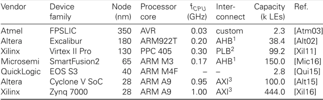
A far more popular option, especially among vendors of conventional standalone FPGAs, are fine-grained, loose coupled systems. Even though microprocessors can be viewed as a recent trend in the evolution FPGA architectures, similar systems were already present more than a decade ago. Modern incarnations have exploited technology scaling to com-bine high-capacity fabrics with more powerful microprocessors. An overview of existing entry-level systems and their predecessors is given in table 2.1.
2.2 FPGA Architecture
Table 2.1:Entry-level commercial systems with loose coupled FPGA fabrics
Vendor Device Node Processor fCPU Inter- Capacity Ref.
family (nm) core (GHz) connect (k LEs)
Atmel FPSLIC 350 AVR 0.03 custom 2.3 [Atm03] Altera Excalibur 180 ARM922T 0.20 AHB1 38.4 [Alt02] Xilinx Virtex II Pro 130 PPC 405 0.30 PLB2 99.2 [Xil11] Microsemi SmartFusion2 65 ARM M3 0.17 AHB1 150.0 [Mic16] QuickLogic EOS S3 40 ARM M4F – – 2.8 [Qui15] Altera Cyclone V SoC 28 ARM A9 0.95 AXI3 100.0 [Alt15] Xilinx Zynq 7000 28 ARM A9 1.00 AXI3 444.0 [Xil16]
1AMBA High-performance Bus 2Processor Local Bus
3Advanced eXtensible Interface
Loose coupling of conventional FPGA fabrics through standardized interconnects and reuse of IP-based microprocessor designs allows such systems to be constructed with minimal effort. Additionally, vendors can rely on mature CAD tools from their main product lines and exploit software ecosystems, including complete operating systems, of dominating ISAs. Other commercial vendors with custom designed fabrics, CAD tools, and integration schemes seem to have had less success [TAJ00, Arn05].
2.2 FPGA ARCHITECTURE
FPGA technology evolved from mask programmable gate arrays and has largely replaced other families of programmable logic. In over 30 years, a variety of FPGA architectures have been proposed and implemented. The following will provide a rough classification of FPGA architectures based on their programmability and their global routing network.
Configuration bits which ultimately define the functionality of a circuit are stored in mem-ory cells alongside routing resources and logic elements of an FPGA. The characteristics of these cells have a direct impact on the overall architecture. The most mature and cur-rently dominating architectures use volatile static random access memory (SRAM) cells. To avoid reconfiguration at each power cycle from external non-volatile memory chips and possible disturbance of the configuration state (soft errors), other approaches directly inte-grate non-volatile memory cells on the same die [Alt16] or within the fabric itself [Act07]. These are niche products due to substantial effort of integrating the non-volatile devices with conventional complementary metal oxide semiconductor (CMOS) processes and significant reduction in logic density. Since SRAM-based FPGAs directly benefit from technology scal-ing, they have been and still are the focus of industrial and academic research. Nonetheless, architectures based on emerging non-volatile memories, which promise high density, seam-less integration with CMOS logic, and low power operation, could become more viable in the future [XZC+11].
The global routing architecture plays an important role, since it is the major contributor to overhead in silicon area, power consumption and delay. Row-based architectures, which mimic mask programmable gate arrays, only provide routing resources in one direction. Logic blocks are connected by routing tracks in adjacent rows and might contain dedicated hard-wired connections between rows. Although this approach can be used to efficiently implement datapaths and reduce mapping complexity, it is restricted to a fixed word length and limited routability might render irregular logic infeasible to map.
rout-2.2 FPGA Architecture
ing network, but impose a muti-stage structure onto the network. Based on the observation that circuits tend to have only a limited connectivity between nodes, a fixed number of LEs are grouped together and are directly connected. This structure recursively connects other groups and forms a hierarchy. Given a custom place and route tool and compatible logic elements, this approach can significantly reduce the overhead and even reuse modern com-mercial front-end tools for synthesis and logic optimization [Wan13]. The major drawback is, again, that the imposed structure restricts flexibility and the irregular structure of the rout-ing network requires large custom layouts. Additionally, scalrout-ing the array capacity requires redesign of the routing network to balance the hierarchy.
Mesh-based or island-style architectures are popular in commercial implementations and have enjoyed the most attention from research. They extend row-based architectures to form a two-dimensional network of routing channels without restricting routability in a par-ticular direction. Each tile, containing logic elements and their local interconnect, is symmet-ric and has the same number of connections to the global routing network. This reduces custom design to one instance of a tile and allows scaling of array capacity by increasing the number of tiles in a rectangular placement. Still, adequate flexibility in the routing network requires a carefully chosen amount of routing tracks. However, many methods have been researched and shown to effectively reduce area overhead without substantial reduction of routability or performance. Many academic tools, including the versatile place and route (VPR) tool, primarily support island-style architectures. A discussion of island-style architec-tures and implementation details of VPR can be found in [BRM99]. Combinations of mesh and tree networks have been adopted in at least one commercial FPGA architecture.
Due to the advantages of simpler physical design, high routing flexibility, and the availabil-ity of open design tools, SRAM-based FPGAs with an island-style architecture were chosen for this thesis. The following discussion of logical parameters for such FPGAs is geared towards structures that are directly supported by the CAD tools.
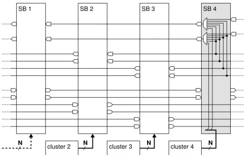
2.2.1 GLOBAL ROUTING NETWORK
A schematic of a global routing network for island-style architectures is shown in figure 2.2. The highlighted section shows the components of a tile: two connection blocks (CBs), a switch block (SB) and the logic cluster. This definition also includes the vertical and hori-zontal routing tracks that form the respective routing channels. To allow external signals to enter the routing network, IO blocks have to be provided at the edges of the array. For stan-dalone FPGAs these blocks represent pad cells and for eFPGAs they represent the system interface of signals routed into the macro. Based on external requirements, these blocks allow a certain number of signals to enter the array (IO capacity) and are placed on specific positions on array perimeter (IO placement). The array is further characterized by the total number of tiles, which limits the size of possible user circuits, and the aspect ratio of the tile arrangement. The latter has to be considered during top-level integration of eFPGA macros. Routing channels are uniformly occupied by a fixed amount of routing tracks and accordingly have a channel width W. This is a crucial parameter as the fixed supply of routing tracks directly influences the quality of mapped circuits and has to be determined at design time of the fabric. It also critically influences the design of the SBs, which are placed at inter-sections of vertical and horizontal channels and allow routed signals to change direction. Historically, routing tracks were driven by tri-state buffers to implement bidirectional routing with signals traveling in both directions of a track. This so-called multi-driver routing allowed identical treatment of cluster inputs and cluster outputs. In modern FPGAs, this design style has been replaced with single-driver routing and unidirectional routing tracks. A direct comparison has suggested that single-driver routing is superior in most aspects [LLTY04]. Due to the single-driver topology chosen in this work, SBs also act as entry points for the
2.2 FPGA Architecture
logic cluster outputs. To feed the logic cluster with inputs from the global routing network, CBs are placed at the vertical and horizontal edges. Restricting tiles to connections with one SB and two CB represents a special case. Better routability could be achieved by allowing connections of the logic cluster to all adjacent channels, however, this increases design and modeling effort, since tiles at the edges would violate the symmetry.
Figure 2.2:Island-style global routing network and fundamental parameters
Figure 2.3:Uniform segmented routing with W = 12, L = 3, and no depopulation; only horizontal routing and taps for one direction are shown
Another important parameter, the segment length L, defines how many tiles a certain segment can span. Segmented routing allows to reduce the number of multiplexer per SB
2.2 FPGA Architecture
and increases the number of direct connections between SBs. Symmetry of the tile is pre-served by staggering track endpoints with respect to the segment length as shown in figure 2.3. The figure also shows the internals of the highlighted SB to visualize how additional connections are tapped off from passing routing tracks and how logic cluster outputs are integrated. To further reduce the size of multiplexers inside SBs, not all possible connec-tions from passing tracks have to be implemented. This so-called depopulation is especially advantageous for circuits that do not require full routing flexibility. A similar method can be used to reduce the number of tracks that are connected per cluster output. Finally, elabo-rate routing networks employ segmentation with multiple segment lengths at once. This mirrors the idea of signal hierarchies but requires significant design effort and again breaks symmetry for tiles near the perimeter. Looking at one particular track inside of a SB, it is also necessary to specify how flexible the SB is, i.e., in how many directions the signal can be routed and to which start points within the channel it can reach. The number of directions is described by the switch block flexibilityFS and the pattern by the switch block topology.
Previous research has identified Wilton switch blocks [Wil97] with flexibility ofFS = 3 to be
appropriate, hence these values are used here. A detailed study of switch blocks and their connection patterns, although targeted at multi-driver architectures, is described in a book by Lemieux and Lewis [LL04].
2.2.2 LOCAL ROUTING AND LOGIC ELEMENT
Just as important as the global routing network are the structures and the parameters that describe the clustered logic elements. The cluster structure assumed here, together with the most important parameters, is shown in figure 2.4.
Figure 2.4:Routing inside the logic cluster and structure of logic elements
ClusteringN LEs together allows local feedback between elements without requiring ac-cess to the slow global network. Each LE has K inputs and two separate outputs. Any combinational logic function with a fan-in less than or equal toK can be implemented with the K-LUT and its output can be feed into the flip-flop to implement sequential logic. Nev-ertheless, this structure with one single-output K-LUT and a flip-flop is very primitive com-pared to state-of-the-art commercial FPGAs, which contain fracturable LUTs with multiple outputs, sophisticated carry and shift logic, and multiple flip-flops. The input of each logic element is driven by a crossbar that implements individual selection of K inputs for each logic element from the available signals, which consist of global inputs and feedback from local LE outputs. As before, routing flexibility may be unnecessary for specific applications
2.2 FPGA Architecture
and hence reducing the flexibility of the crossbarFc,local can provide another option for area
reduction [LL01]. To route signals into the cluster, I inputs are provided by the CBs. The number of cluster inputs has to be chosen such that all logic elements can be fed with suf-ficient global signals. Providing too few inputs reduces the effectiveness of clustering and forces the routing algorithm to leave logic elements unused. Early research has empirically derived the following rule of thumb to ensure high utilization (>98 percent) of logic elements [Ahm01]:
I= K
2 (N+ 1) (2.1)
The number of cluster inputs directly defines the number of all multiplexers within CBs of a tile, where each multiplexer allows a fractionFc,inof all routing tracks (including those
with-out endpoints at this tile) to connect to one of the cluster inputs. Likewise,Fc,out describes
the fraction of routing tracks that can be reached by a cluster output.
The previously described logical architecture is restricted to homogeneous FPGAs, which are constructed from a number of identical tiles with identical function. The primary motiva-tion for this restricmotiva-tion is that it enables a homogeneous global routing network, described by only a few numerical parameters, but also simplifies the task of FPGA design and lay-out. Recent architectures, studied in research or present in commercial devices, contain more advanced fabrics with heterogeneous components such as memory blocks, dedicated multipliers, and hardware support for IO protocols. Also, fabrics employed in the systems presented in section 2.1.2 have extended logic element structures and local interconnects to explicitly support arithmetic operations. However, integration of heterogeneous blocks into the global routing network or arithmetic enhancements of the logic elements require a thorough understanding of the tradeoffs and interdependencies within the baseline hetero-geneous architecture. Only a limited number of design decisions can be guided by intuition or designer experience and the vast design space spanned by the previously described log-ical parameters necessitates a comprehensive exploration.
3 FPGA ARCHITECTURE EXPLORATION
Faced with a large set of possible logical architectures and no guidance to select them in the context of a 22 nm process technology, a comprehensive design space exploration was conducted. The goal was not only to find architectures suitable for a tight coupled instruc-tion set extension, but also to characterize them regarding implementainstruc-tion cost and perfor-mance. This chapter presents the methodology for this exploration including the employed CAD tools, transistor level implementations, the area model, and the selection of logical parameters. Also, results are presented and discussed by comparing them with previous explorations.
3.1 PRELIMINARIES
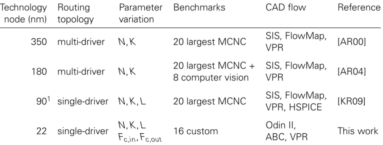
While analytical models have been proposed for a similar task [DLW+11, HWY+09], their ap-proach was unsuited for the chosen process technology. Nevertheless, they provide a help-ful reference for general insights and discussion of parameter interdependencies. Hence, SPICE simulations are regarded as the most accurate form of estimating performance. Only a few comprehensive explorations have been performed to study the impact of the most important logical parameters on FPGA performance and area efficiency. Results from these studies are quoted frequently to justify architectural decisions without respecting the con-text in which these results have been obtained. Table 3.1 lists important details of the most commonly referred to design space explorations for logical FPGA architectures.
Table 3.1:Comparison of design space explorations for logical FPGA architectures
Technology Routing Parameter Benchmarks CAD flow Reference node (nm) topology variation
350 multi-driver N, K 20 largest MCNC SIS, FlowMap, [AR00] VPR
180 multi-driver N, K 20 largest MCNC + SIS, FlowMap, [AR04] 8 computer vision VPR
901 single-driver N, K, L 20 largest MCNC SIS, FlowMap, [KR09] VPR, HSPICE
22 single-driver N, K, L 16 custom Odin II, This work
Fc,in, Fc,out ABC, VPR
1Multiple technologies studied using predictive models [CSO+00].
For the purpose of this study, modern CAD tools, an advanced process technology, and a set of custom benchmarks, representative of typical datapath circuits, were used. Results from previous explorations are not applicable in the context of this thesis, since they used benchmarks and cost functions aimed at general purpose applications. All previous studies listed in table 3.1 relied on SIS [SSL+92] and Flowmap [CD94] for logic optimization and
3.1 Preliminaries
technology mapping, both of which have since been superseded. Furthermore, these stud-ies only reported results in terms of area or delay, but did not include critical information on configuration overhead or circuit topologies. Still, their results are useful to prioritize the selection of parameters according to their interdependencies. Additionally, they have established certain guidelines on how to define and measure a figure of merit for FPGA architectures. Also, they provide reference results that can be used to compare the relative impact of a parameter on that figure.
3.1.1 CAD TOOLS
Figure 3.1 gives an overview of the steps and CAD tools that have been used during the exploration. Most of these tools were afterwards reused to map circuits of custom instruc-tions onto the final FPGA architecture.
Figure 3.1:Extended Verilog to Routing CAD flow, original steps highlighted
The majority of this flow relies on the VTR project [LGW+14], which combines various
open-source tools to provide a complete flow that maps a user circuit, described with Ver-ilog, onto a parameterizable FPGA architecture.
Odin II [JKGS10] is used to parse the RTL description of the user circuit, synthesize high--level expressions, and produce a netlist in the Berkeley logic interchange format (BLIF) that can be read by subsequent tools. Unfortunately, Odin II has proven to be a major
impedi-3.1 Preliminaries
ment. First, it only supports a very limited subset1of Verilog, which makes it hard to reuse already designed and verified components or to develop new RTL circuits. As this thesis deals with mostly small and manageable circuits, these restrictions are regarded merely as annoyances. However, it might be impractical to describe circuits in a supported for-mat once larger designs and fabrics with higher capacity are used. Second, since Odin II also supports to detect and replace arithmetic functions with heterogeneous blocks, it pro-duces poor synthesis results if the target architecture does not contain such elements (es-pecially multipliers). Other researchers have identified similar problems with Odin II [Hun15] or sidestepped them using commercial tools for front-end synthesis [MWL+15]. Third, and
more dramatically, it is easy to describe circuits that will lead to synthesis mismatch, that is, Odin II produces a netlist that isfunctionally incorrect. Synthesis mismatch is also possible with other tools, as Verilog purposely allows non-synthesizable constructs, however, the example in listing A.1.4 is extremely simple and unambiguous. The discrepancy is directly apparent from the synthesized BLIF netlist in listing A.1.5 and has also been verified with a correctly synthesized netlist produced by a commercial tool2. To nonetheless make use of
the VTR flow and ensure correct behavior in this work, user circuits were carefully designed and all application benchmarks were verified with the approach described in section 5.2.
The next step in the CAD flow consists of logic optimization and technology mapping to
K-LUTs, which is accomplished using ABC [Ber16] and a corresponding command script. ABC is a framework for analyzing and modifying sequential logic circuits, predominantly us-ing and-inverter graphs, and can be regarded as the successor of SIS. It provides a large variety of algorithms for logic optimization, technology mapping, and formal verification. Re-grettably, complete end-to-end verification of the post-routing netlist with the RTL descrip-tion using ABC was not possible, since the circuit first had to be synthesized by Odin II. Using a hybrid academic and commercial flow, it has been shown that ABC on its own is capable of producing high-quality results, on a par with a modern commercial FPGA CAD suite [VKF15].
The mapped BLIF netlist produced by ABC and a description of the FPGA architecture is afterwards fed into the versatile place and route tool [BR97]. Since its introduction, VPR has become the de facto standard platform for research on island-style FPGAs. Due to its permissive and open-source licensing, many extensions have been contributed to improve its flexibility and to improve its support for modern heterogeneous FPGA architectures. A flexible description language [LAR11], based on XML, allows description not only of the log-ical FPGAs architecture but also of configurable and physlog-ical characteristics of fundamental building blocks. This description is used during packing to group LUTs from the netlist into logic clusters and to determine the assignment of local interconnect resources. Based on the amount of occupied clusters, a square array of tiles with sufficient capacity is automat-ically determined by VPR. A user-defined placement of IO resources can be provided to specify the location of design signals on the array perimeter. Otherwise, the assignment of IO blocks is automatically determined by the placement algorithm. Afterwards, the packed netlist is placed onto the array with a simulated annealing algorithm. During timing-driven placement, VPR assigns each packed cluster a position within the array while trying to min-imize the cost in terms of delay, estimated from distances between tiles [MBR00]. Once a legal placement has been determined, VPR proceeds with timing-driven routing, using the Pathfinder algorithm [ME95]. This procedure first routes the design without considering congestion and then repeatedly rips up and reroutes critical connections. Convergence to-wards a feasible routing is archived by gradually increasing the cost weight for congestion. Crucial for congestion and the success of routing is the channel widthW, which is either
1Unsupported: module parameters, generate statements, variable bit shifts, multi-dimensional wires, arrays of instances, combinational overriding, complex expressions within concatinations.
3.1 Preliminaries
provided by the user or automatically determined by VPR with multiple routing trials. Finally, timing analysis on the routed design is performed and a timing annotated post-rout-ing netlist is generated together with a detailed report on cluster usage, channel occupation, and critical path length. The post-routing netlist can subsequently be used to inspect the behavior of the routed design with a conventional Verilog simulator. Fine-tuning of all steps within VPR is possible by overriding a set of default options. Additionally, to allow experi-ments with different implementations of the employed algorithms, it is possible to intercept the output of all stages and to provide inputs from other tools. Access to VPR’s internal rep-resentation of the routed netlist makes it possible to generate configuration bitstreams for specific physical implementations of an FPGA architecture. Bitstream generation for se-lected Xilinx architectures is possible with the extension presented in [HEW13], however routing and bitstream generation still rely on tools from the vendor.
When VPR was first introduced, no detailed physical models of FPGAs were available so that many crude sizing rules were incorporated to reflect the influence of different logical architectures on performance or occupied area. Detailed descriptions of the built-in models and assumptions within VPR are described by its original authors in a book [BRM99]. In particular, they developed the minimum-width transistor area (MWTA) model to estimate the required area for full custom layouts of different FPGA leaf cells. This model estimates total area by counting scaled versions of a transistor with minimum width. For loads that require stronger drivers, a linear relationship between driving capability and the width of a transistor is established. Furthermore, it assumes that the layout area is dominated by the active area of transistors and that additional area for routing can be neglected. MWTAs are frequently used to express the size of FPGA tile components in a technology independent unit. In the current version of VPR, the architecture description provides options to override most of those built-in assumptions with absolute timings or concrete values of occupied area. However, it still contains hidden and poorly documented assumptions that try to estimate transistor sizes, especially for routing tracks, with unjustified load models and assumptions about the size of memory cells.
As this exploration was intended to provide reasonable estimates of delay and area for FPGA components in a commercial 22 nm process technology, the original VTR flow was extended prior to the exploration phase. To reflect the physical characteristics of different logical architectures, a detailed transistor level model was adapted from a tool for fully-auto-matic sizing of FPGA tiles [Chi13]. COFFE, which stands for "Circuit Optimization For FPGA Exploration", was primarily developed as an alternative to a similar tool for automatic transis-tor sizing previously developed and described by Kuon [KR09]. Most importantly, COFFE is capable of generating SPICE testbenches of individual tile components together with proper loads according to the parameters of a logical FPGA architecture. This allows the tool to es-timate delay and layout area of all necessary building blocks. Once a tile is characterized, the defining physical properties are used to annotate the architecture description which is subsequently used by VPR.
COFFE estimates layout area based on the width of individual transistors and a modified MWTA model, fitted to area data obtained from layouts in a 65 nm technology. The quality of this new model cannot be assessed objectively since the basis for fitting as well as the factor for subsequent scaling to a 22 nm technology are not documented. Detailed modeling of the circuit topologies allows COFFE to calculate concrete values for area overhead due to configuration memory, where a single-bit cell is assumed to occupy 4 MWTAs. Based on the estimated areas, COFFE attempts to include interconnect parasitics with a lumped RC model. Wire length is estimated from simple connectivity rules and the assumption that all cell layouts are square. Process specific data in terms of transistor models together with sheet resistance and interconnect capacitance for the metal layers are read into COFFE from a file.
3.1 Preliminaries
The logical FPGA architecture is specified by an additional file containing the set of logical parameters that describe one tile of a homogeneous FPGA. Tiles are modeled as described in section 2.2, i.e., each tile consists of one switch block, two connection blocks and one logic cluster. All routing channels have the same channel width and employ single-driver routing. COFFE supports depopulation in the connection blocks and in the cluster cross-bar. Logic elements have the architecture shown in figure 2.4 with the addition of optional feedbacks from the local output directly into one LUT input. However, this feature is dis-abled and not further explored in this thesis, as it introduces asymmetry in the layout of LUTs and requires additional overhead in the form of a multiplexer and configuration mem-ory. Additionally, COFFE’s more flexible logic elements are restricted to one local and one global output, while the flip-flop is always driven by the single output of the LUT. Next, the underlying transistor level implementations of the tile components are described.
3.1.2 TRANSISTOR LEVEL IMPLEMENTATION
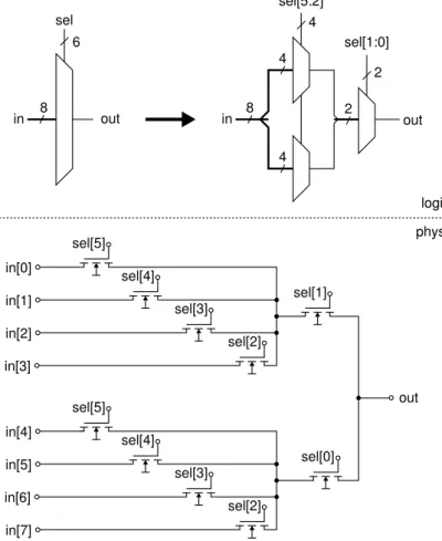
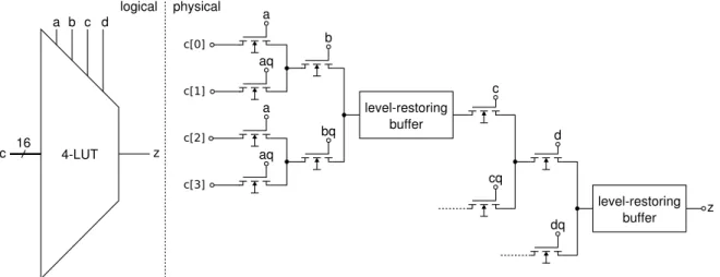
To allow characterization of delays with SPICE simulations, COFFE also includes a library of circuits that implement all necessary tile components. Emphasizing modularity, the library composes larger circuits from a set of basic components, including a pi-shaped segment for wire loads, an inverter, a level-restorer, an NMOS pass gate, and a transmission gate. Here, the transmission gate is unused and instead pass gates are used exclusively to implement multiplexer structures. 8 sel 6 out sel[5:2] sel[1:0] 4 2 2 8 4 4 out in in out logical physical sel[0] sel[1] sel[2] sel[4] sel[3] sel[5] sel[2] sel[4] sel[3] sel[5] in[3] in[2] in[1] in[0] in[4] in[5] in[6] in[7]
Figure 3.2:Logical views and two-level pass gate implementation of a 8:2:1 routing multiplexer
In fact, due to the homogeneous and symmetric nature of the FPGA tiles, multiplexers are sufficient to implement all necessary logical components, except for flip-flops. Routing
3.1 Preliminaries
multiplexers and LUTs represent the two different classes of multiplexer structures and each require different circuits to ensure area efficient implementations.
Routing multiplexers can be used to directly implement connection blocks, switch blocks and the crossbar. Configurable routing is achieved by attaching the outputs of memory cells to the select inputs of the multiplexer shown in figure 3.2. The output signal can thus be selected from any of the input signals by programming an appropriate configuration pattern into the memory cells. The figure also shows the pass gate network employed by COFFE to implement routing multiplexers. Although two-level multiplexer structures require more configuration bits, they provide fast operation by allowing only one pass gate per stage to be enabled by using a one-hot configuration scheme. Other schemes with less configuration bits would require additional overhead for decoding or would introduce more than two pass gates in the path of the routed signal. A special case is represented by the output selection multiplexer of the logic element. Since the described architecture of the logic element is very simple, only two signals need to be routed. This can be achieved with a single configuration bit and two pass gates in parallel, assuming the memory cell provides two complementary outputs.
To implement combinational logic, the aforementioned routing structures connect multi-ple LUTs, each generating a single output bit in response to a multi-bit input pattern. Using this approach, LUTs represent direct implementation of Boolean functions and their truth-ta-bles. By storing all possible outputs within memory cells and arranging them at the input of a multiplexer, K-LUTs can implement arbitrary logic functions, limited only by the inputs of the logic function. Figure 3.3 shows how a pass gate LUT with four logical inputs is implemented in COFFE.
Figure 3.3:Logical and truncated physical view of a 4-LUT
In contrast to a routing multiplexer, the LUT must provide minimal delay through the select inputs of the multiplexer. The other inputs are driven by the quasi-static outputs of the configuration memory. Thus, a binary tree structure is used in which each select signal drives two complementary branches of the tree. To select only one lookup value at a time, the logical select inputs must be available in inverted and non-inverted form (e.g.,aqanda). Again, this structure was chosen so that the critical path through the select inputs contains no unnecessary decoders.
On one hand, pass gate implementations offer very compact implementations of the previously described structures. On the other hand, they require special signal buffering to restore the full signal swing. The signal level at the output of pass gates using NMOS transistors is reduced by the required threshold voltage drop across the gate and source terminals. Multiple series pass gates, as shown in figure 3.3 for the LUT, can reduce the

![Figure 2.1: Mesh routing network of the EGRA [ABP11] (© 2011 IEEE)](https://thumb-us.123doks.com/thumbv2/123dok_us/1079599.2643686/13.892.275.644.530.861/figure-mesh-routing-network-egra-abp-ieee.webp)